

Audioprocessor TDA 4390-2X
1 Overview
The TDA 4390-2X is a single-chip audio sound system.
The circuit can be partitioned into two functional
blocks.
P-DSO-28-3
1.1 Features
1. Stereo sound processing
• Four stereo AF inputs
• Input/Output interface for external equalizer
• Max. gain switchable between 0 dB and 6 dB
• Bass and treble control
• Four independent attenuators for volume balance and fader control
2. Control part
2
• I
C Bus interface compatible for standard and fast mode
• Control of sound processing
Type Ordering Code Package
TDA 4390-2X Q67000-A5183 P-DSO-28-3
Semiconductor Group 1 02.96
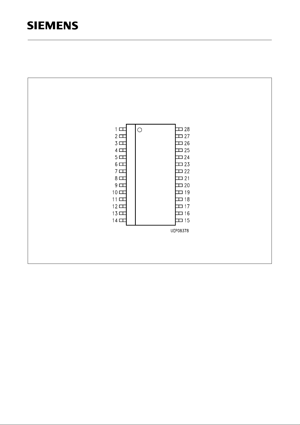
1.2 Pin Configuration
(top view)
TDA 4390-2X
P-DSO-28-3
Figure 1
Semiconductor Group 2 02.96
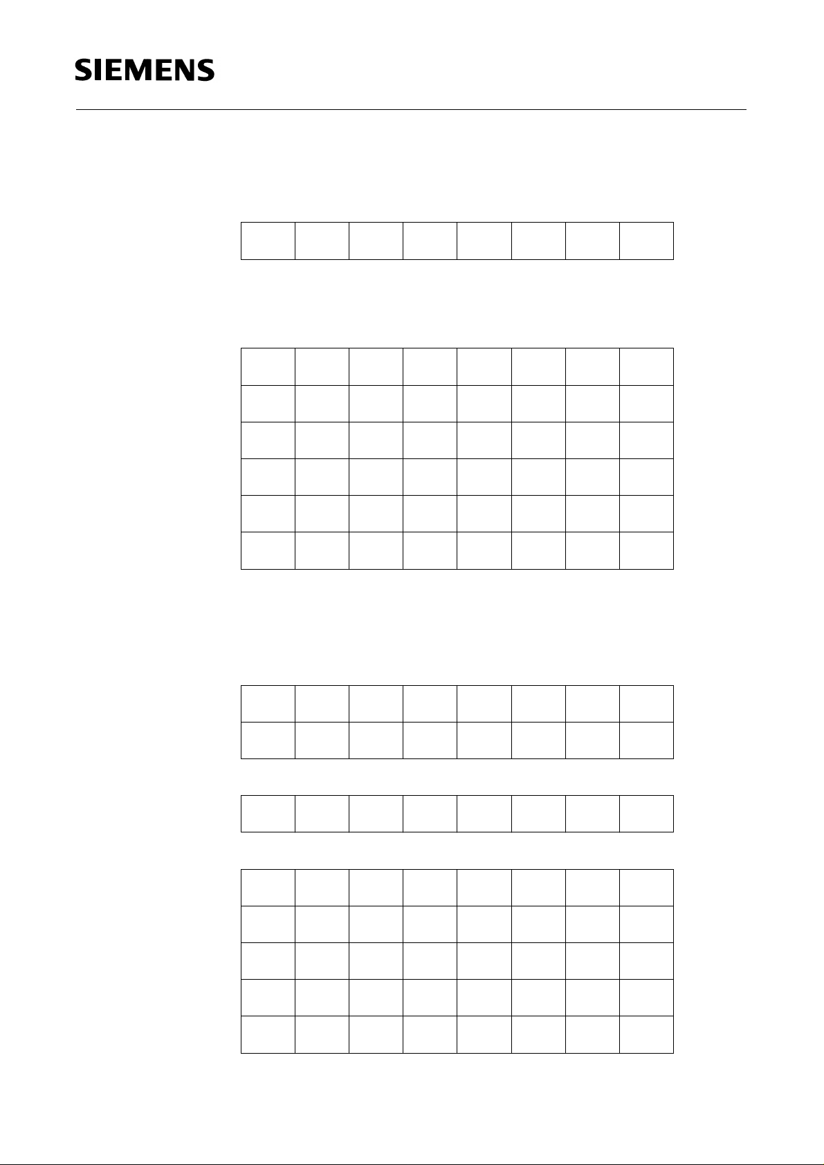
1.3 Pin Definitions and Functions
Pin No. Symbol Function
1 AF input 1 left
2 AF input 2 left
3 AF input 3 left
4 AF input 3 left
5 AF output switch left
6 AF input tone control volume left
7 Reset (all functions in power ON status)
8 I
9 I
2
C Bus SCL
2
C Bus SDA
TDA 4390-2X
10 Supply voltage
11 Corner frequency treble left
12 Corner frequency treble right
13 AF output right front
14 AF output right rear
15 AF output left rear
16 AF output left front
17 Corner frequency bass right output
18 Corner frequency bass right input
19 Corner frequency bass left output
20 Corner frequency bass left input
21 Ground
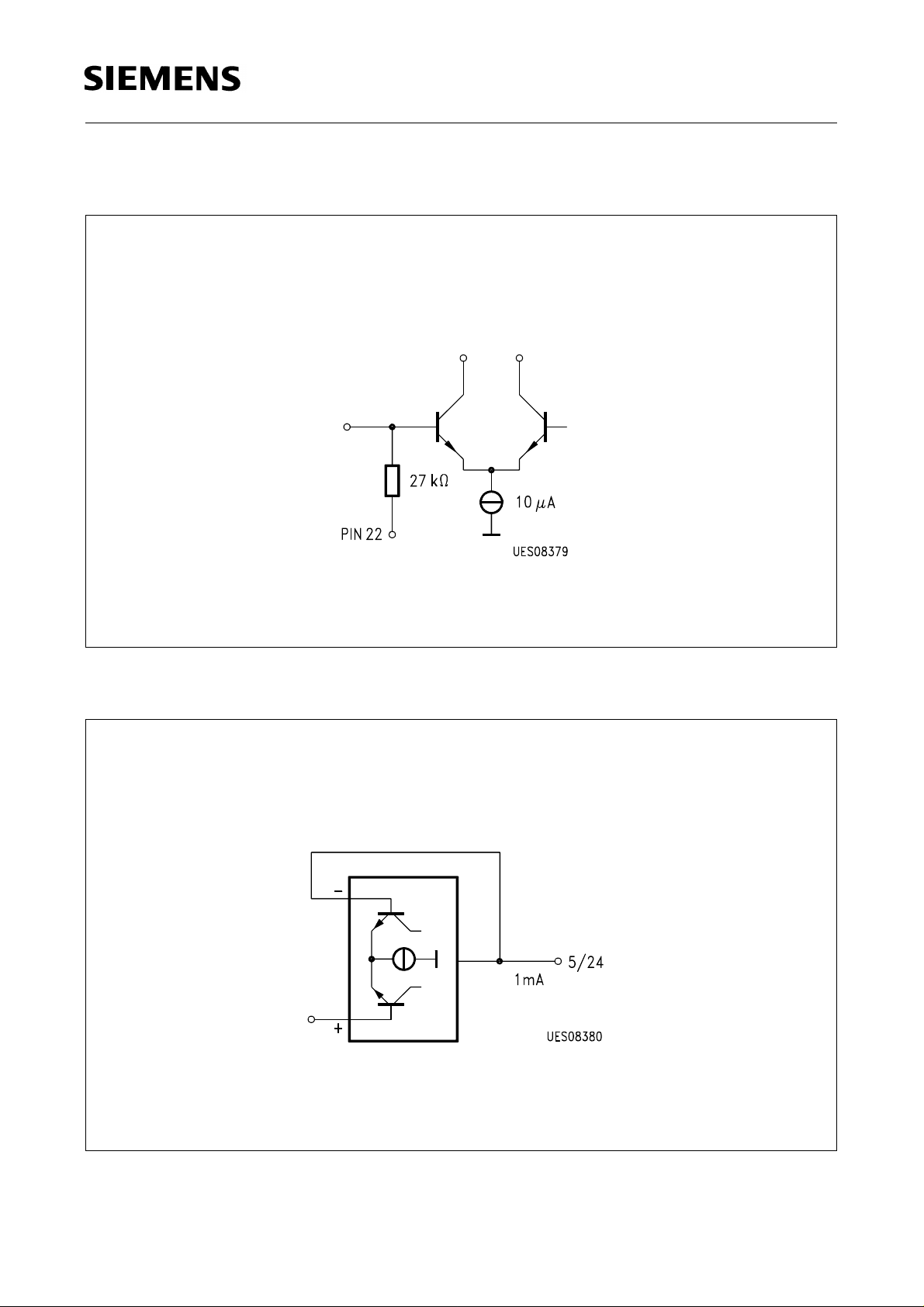
22 Blocking AF operating point
23 AF input tone control volume right
24 AF output switch right
25 AF input 4 right
26 AF input 3 right
27 AF input 2 right
28 AF input 1 right
Semiconductor Group 3 02.96
1.3.1 Pin Description
TDA 4390-2X
Figure 2
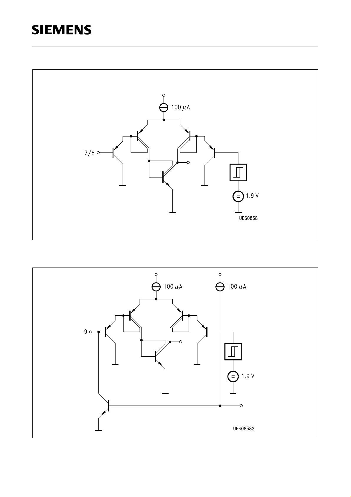
AF Inputs PIN 1/2/3/4/6/23/25/26/27/28
Figure 3
AF Outputs PIN 5/24
Semiconductor Group 4 02.96
TDA 4390-2X
Figure 4
Reset PIN 7, I
2
C Bus SCL PIN 8
Figure 5
I2C Bus SDA PIN 9
Semiconductor Group 5 02.96
TDA 4390-2X
Figure 6
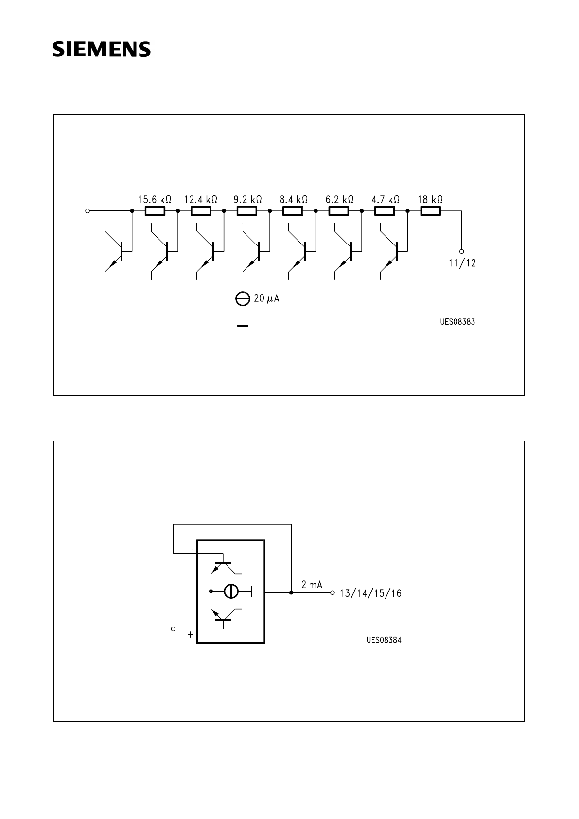
Corner Frequency Treble PIN 11/12
Figure 7
AF Outputs PIN 13/14/15/16
Semiconductor Group 6 02.96
TDA 4390-2X
Figure 8
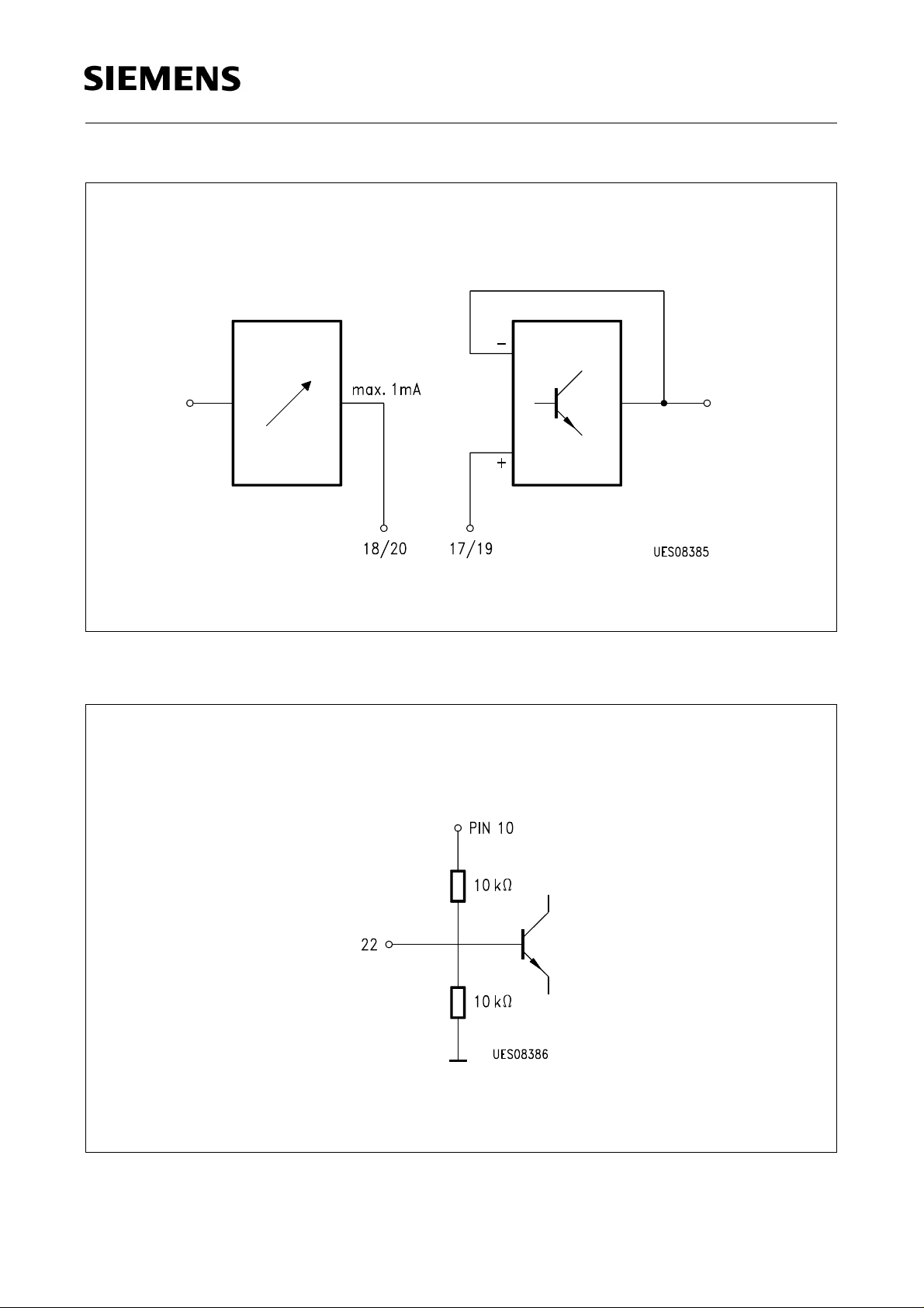
Corner Frequency Bass PIN 17/18/19/20
Figure 9
AF Operating Point PIN 22
Semiconductor Group 7 02.96
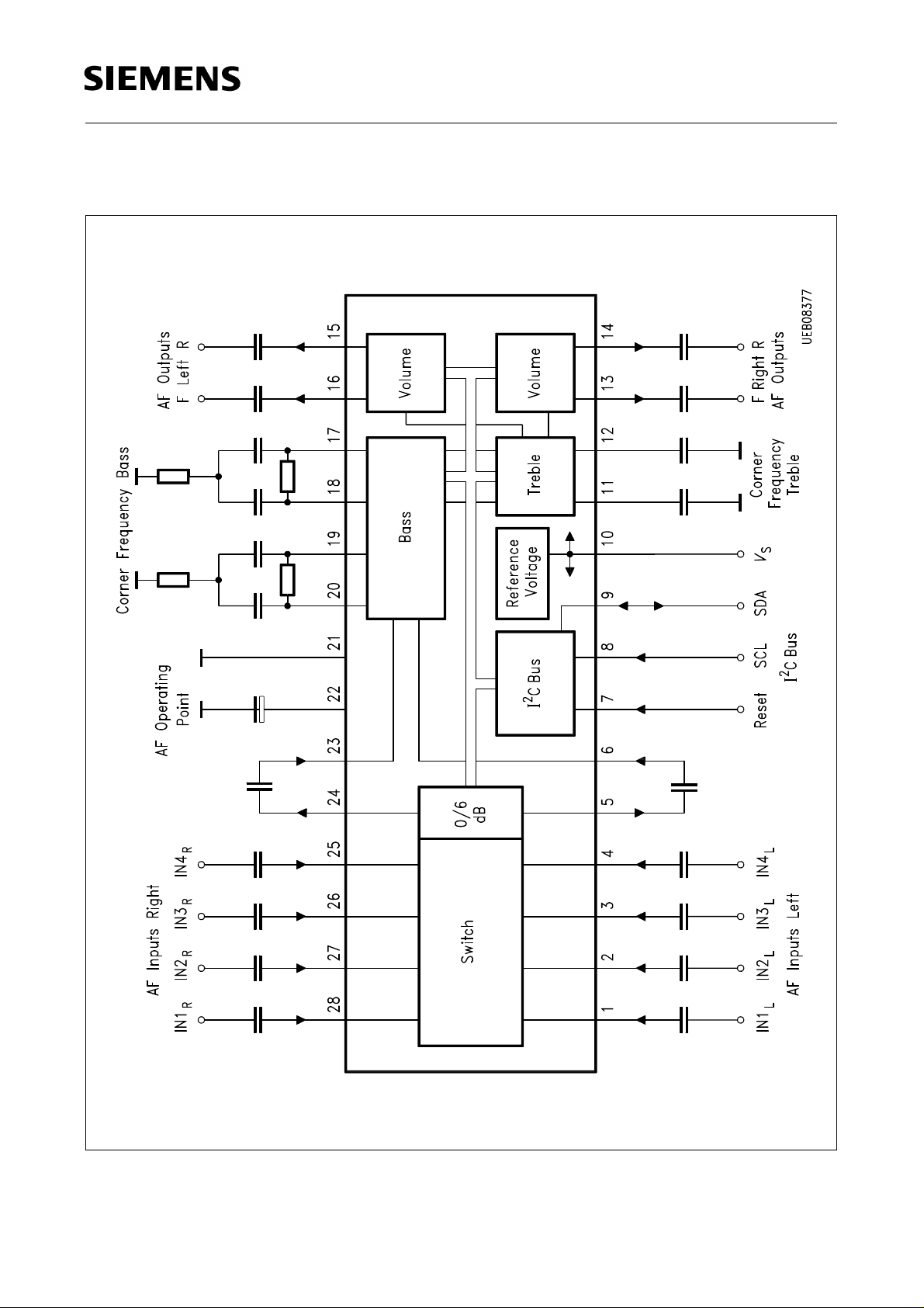
1.4 Functional Block Diagram
TDA 4390-2X
Figure 10
Block Diagram
Semiconductor Group 8 02.96

TDA 4390-2X
2 Circuit Description
2.1 Signal Processing
1. The selection of the AF inputs happens in the input switch. There are four stereo
inputs available. An input level switch circuitry behind the input switch realizes the
adaption of different signal source levels. A gain of 0 dB or 6 dB is possible. After this
section a stereo output/input is placed for connecting external circuits like an
equalizer.
2. In the following signalpath there is tone control, consisting of bass and treble control.
Bass control offers a control range of + 18 dB to – 12 dB with a stepwidth of 2 dB.
Frequency characteristic, 1st order or 2nd order (resonance type) is fixed by external
components. Treble control offers a control range of ± 12 dB with a stepwidth of 2 dB.
The treble control corner frequency is fixed by an external capacitor. Last stage in
signalpath is volume control which can be adjusted independent for left, right, rear and
front. 57 steps with an increment of 1.25 dB give a setting range of 70 dB, the 57th
step activates muting.
2.2 Controlpart
All functions are controlled via an I
2
C Bus interface. All data is stored into a latch circuit.
The telegram structure is built as follows:
Startcondition – chipaddress – any number of databytes – stopcondition.
For the databytes the following conditions must be fulfilled:
first
Before transmitting a databyte a subaddress byte must
be placed in the data
telegram.
Semiconductor Group 9 02.96
TDA 4390-2X
2.2.1 Chipaddress
MSB LSB
10000010
2.2.2 Subaddress bytes
MSB LSB
Volume front left ЧЧЧЧЧ000
Volume front right ЧЧЧЧЧ001
Volume rear left ЧЧЧЧЧ010
Volume rear right ЧЧЧЧЧ011
Bass/treble ЧЧЧЧЧ101
Switchbyte ЧЧЧЧЧ111
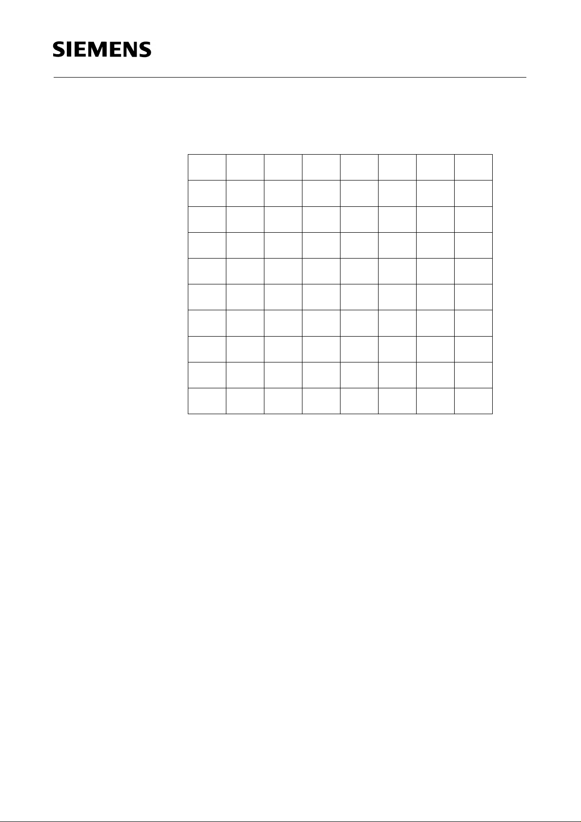
2.2.3 Controlbytes
a) Volume left, right, front, rear
MSB LSB
Max. volume ××111111
Max-1 ××111110
Max-16 ××110000
Max-55 ××001000
MUTE ××000111
MUTE ××000000
MUTE ××000×××
Power ON 0 0 0 0 0001
Semiconductor Group 10 02.96
TDA 4390-2X
b) Treble/Bass
MSB LSB
Linear 1 0 001001
Max. treble, lin. bass 0 0 101001
Max. treble, lin. bass 0 0 0 × 1001
Min. treble, lin. bass 1 1 101001
Min. treble, lin. bass 1 1 1 × 1001
Lin. treble, max. bass 1 0 000000
Lin. treble, min. bass 1 0 001111
Max. treble, max. bass 0 0 0 × 0000
Min. treble, min. bass 1 1 1 × 1111
Power ON 0 0 000001
MSB
treble
LSB
treble
MSB
bass
LSB
bass
Semiconductor Group 11 02.96

c) Switchbyte
TDA 4390-2X
MSB LSB
MUTE IN1 IN2 IN3 IN4 Gain ××
MUTE = 0
MUTE = 1
IN1 = 0
IN1 = 1
IN2 = 0
IN2 = 1
IN3 = 0
IN3 = 1
IN4 = 0
IN4 = 1
Gain = 0
Gain = 1
MUTE OFF; power ON
MUTE ON
Input1 OFF; power ON
Input1 ON
Input1 OFF; power ON
Input1 ON
Input1 OFF; power ON
Input1 ON
Input1 OFF; power ON
Input1 ON
Gain 0 dB; power ON
Gain 6 dB
If no signal is activated, this is interpreted as muting.
There is no mutual lockout of the inputs for multiple selections.
Semiconductor Group 12 02.96
 Loading...