

Dual Conversion AM Receiver TDA 4360X
1 Overview
1.1 Features
• High flexibility with an external preamplifier stage
• Sym. or asym. mixer input
• 2-pin oscillator for the 1. LO
• 1. LO with LC tank circuit
• 1. LO at 100 MHz range
• Low narrow band noise
• Divider for 1. LO by 10 for the 100 kHz … 2 MHz range
and by 8 for the 2 MHz … 6 MHz range
• Integrated AGC generation
• Strictly symmetrical RF path
• Decoupled counter output
• 2. LO with quartz or external source
• Output for gain controlled 2. IF
• Switchable AGC time constant
P-DSO-28-1
Type Ordering Code Package
TDA 4360X Q67000-A5181 P-DSO-28-1
1.2 Application
The TDA 4360X is an integrated dual conversion AM receiver for use in car radios.
The input signal passes a linear mixer for conversion into the 1. IF (~ 10 MHz). Via an
external bandpass filter (CER filter, quartz filter) the 1. IF is converted in a second linear
mixer to the 2. IF (~ 460 kHz).
After an external narrowband selectivity (CER filter) the 2. IF passes an automatic gain
controlled (AGC) amplifier and is then demodulated to the AF. The AGC time constant
can be switched with a ratio of 20.
For counter controlled search tuning stop (STS) the frequencies of the 1. LO and the
2. IF are available.
Semiconductor Group 1 04.96
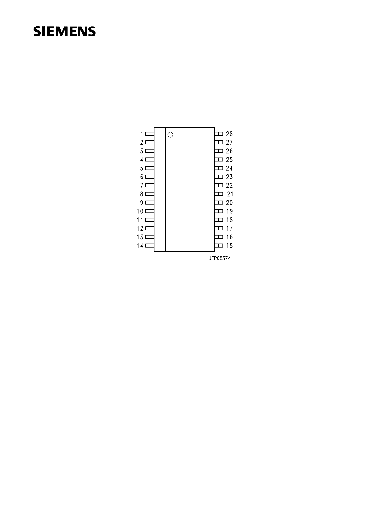
1.3 Pin Configuration
(top view)
TDA 4360X
P-DSO-28-1
Figure 1
Semiconductor Group 2 04.96
1.4 Pin Definitions and Functions
Pin No. Function
TDA 4360X
1, 2
3
4
5
6
7, 8
9
10
11
12
13
Sym. Input for the AM signal in the frequency range of 100 kHz (SW) to 6.2
MHz (49m-Band) sym. application is recommended, asym. application is
possible
DC voltage alters the threshold voltage of the prestage AGC circuit.
GROUND: All DC values are referred to this pin
Buffered output for the by n divided (n = 8 or 10) oscillator frequency
Output for the internal reference voltage. This pin is to be blocked with a
ceramic capacitor to ground.
The ext. LC circuit between pin 7 and pin 8 determines the oscillator
frequency.
Supply voltage. This point is to be blocked to ground for AF and for RF
signals.
Buffered output for the oscillator frequency
Input for the frequency divider. Low voltage to pin 11 divides the oscillator
frequency by 8, high voltage or open input divides by10.
Blocking capacitor for the IF AGC circuit to suppress AF frequencies
Input to select the fast or slow AGC time constant
14
15
16
17, 18, 19
20
21, 22
23, 24
25
26
27, 28
Buffered AF output
Buffered output for the limited lower IF frequency. This signal is necessary
for an IF Counter Tuning System.
Buffered output for the AGC controlled lower IF signal. This pin is connected
to the AM stereo decoder.
Input pins for the DC coupled AGC amplifier
Open collector output of mixer for the lower IF (~ 450 MHz). A DC
connection to the tank circuit to
V
is recommended.
ref
Sym. mixer 2 input for the upper IF (~ 10.7 MHz). Asym. operation is
possible. The input signal is converted to the lower IF corresponding the
equation
f
LIF
= f
UIF
– f
2.LO
.
Input for the 2. local oscillator (LO). The pins can be connected via a quartz
or the oscillator is to be forced with an ext. signal.
Blocking capacitor for the prestage AGC
A capacitor to ground determines the AGC time constant. The DC potential
at this pin can be used for controlling the FET in the ext. prestage.
Sym. collector output of the mixer 1. The external tank circuit is tuned to the
upper IF.
Semiconductor Group 3 04.96
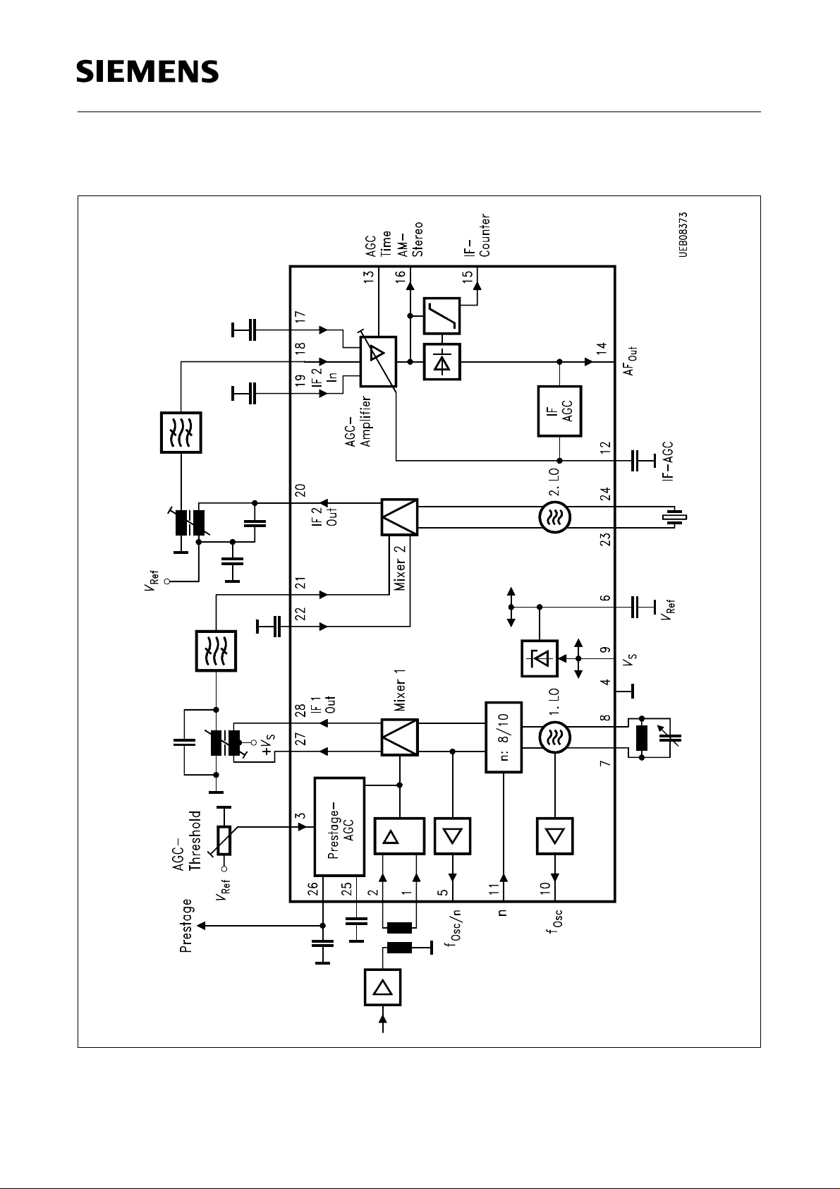
1.5 Functional Block Diagram
TDA 4360X
Figure 2
Block Diagram
Semiconductor Group 4 04.96
 Loading...