

Siemens TDA4350X Datasheet
Audioprocessor TDA 4350X
1 Overview
1.1 Features
Stereo-Soundprocessing
• Three stereo AF inputs, one of the inputs is
equipped with floating ground.
• Input level control for individual level setting of the
several AF sources in addition with a clipping
detector.
• Volume control with software controlled switchable loudness function. Frequency
response fixed by external components.
• Bass- and treble control with clipping detector.
• Four independent settable output attenuators for balance/fader function.
• Fan-out of the AF outputs software controlled.
• AF outputs switchable for driving bride power amplifiers.
2
• I
C Bus controlled immediately, or zero cross detector dependent mute, or
immediately mute via extra pin.
P-DSO-28-1
Control Part
2
C Bus interface
• I
• Control of sound processing
• Read out of the clipping detector status.
Type Ordering Code Package
TDA 4350X Q67000-A5060 P-DSO-28-1
1.2 Application
The TDA 4350X is a single-chip audio-soundsystem. The circuit can be partitioned into
two functional blocks: stereo-soundprocessing and control part.
Semiconductor Group 1 04.96
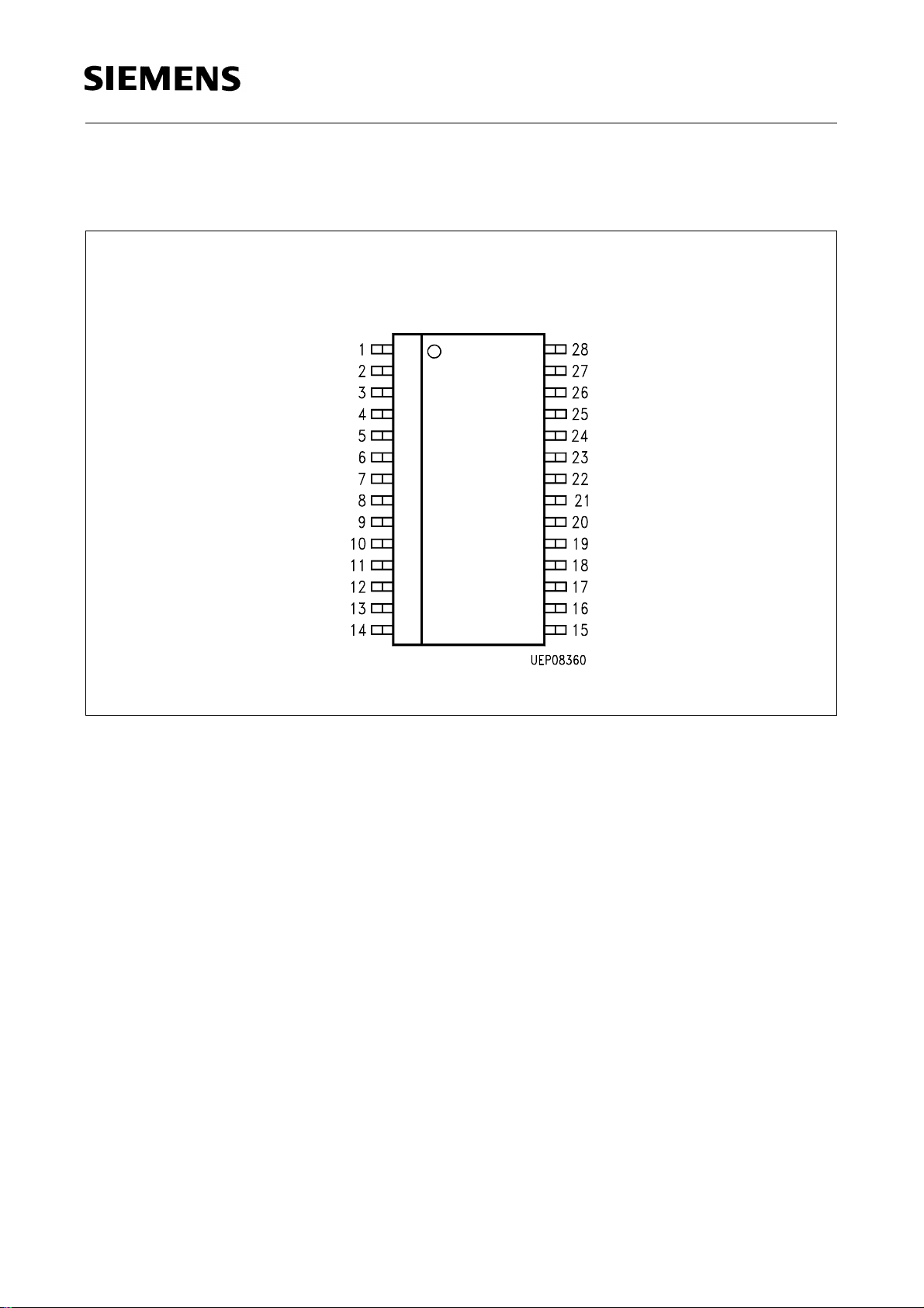
1.3 Pin Configuration
(top view)
TDA 4350X
P-DSO-28-1
Figure 1
Semiconductor Group 2 04.96
1.4 Pin Definitions and Functions
Pin No. Function
1 CD input right
2 Input 2 right
3 Input 3 right
4 Loudness output right
5 Loudness input right
6 Digital ground
7 Mute
8 I
9 I
2
C Bus SCL
2
C Bus SDA
TDA 4350X
10 +
V
supply voltage
S
11 Corner frequency treble left
12 Corner frequency treble right
13 AF output right front
14 AF output right rear
15 AF output left rear
16 AF output left front
17 RC network bass right
18 RC network bass right
19 RC network bass left
20 RC network bass left
21 Analog ground
22 Bias for AF operation point
23 Loudness output left
24 Loudness input left
25 Input 3 left
26 Input 2 left
27 CD ground
28 CD input left
Semiconductor Group 3 04.96
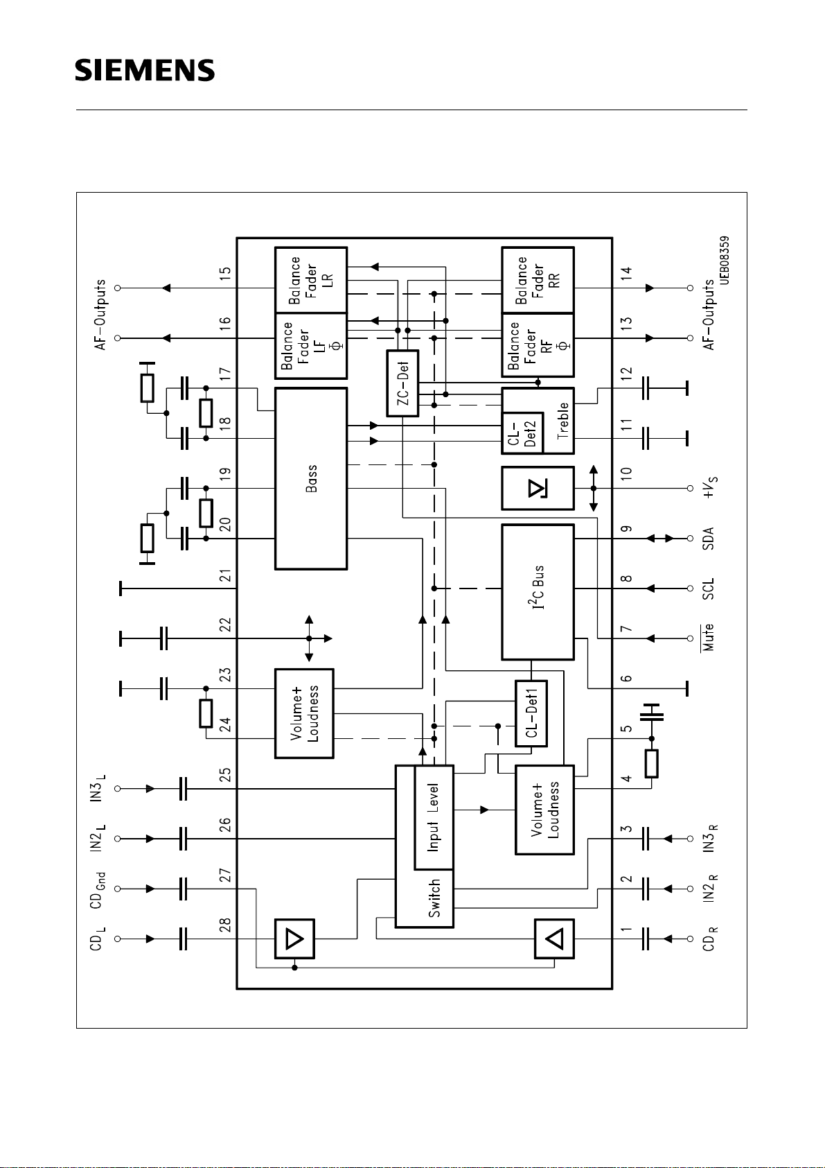
1.5 Functional Block Diagram
TDA 4350X
Figure 2
Block Diagram
Semiconductor Group 4 04.96
TDA 4350X
2 Circuit Description
2.1 Signalprocessing
1. The selection of the AF inputs happens in the input switch. There are three
stereo-inputs available. One of the input pairs is equipped with a separate floating
ground connection especially provided for external signal sources. Crosstalk to this
input is suppressed by common mode rejection. An input level control circuitry behind
input switch realizes the adaption of different signal source levels. The circuit offers a
control range from 0 dB to + 25 dB with a stepwidth of 2.5 dB. An I
first clipping detector allows a software controlled level adaption.
2. Next stage in signal path is volume control, with common setting for both channels, a
control range of 0 dB to – 78.75 dB and a stepwidth of 1.25 dB. In this stage a
loudness function is realized. A loudness control circuit, in fact a second volume
control circuit with identical structure, is to be set to a higher level as volume control.
The resulting level difference fixes the maximum amplitude response of the loudness
function. The frequency response, only bass boost or combined bass and treble boost
is fixed by external components. Because the volume and loudness control are strictly
independent of each other, the frequency response and threshold of the loudness
function is programmable via software. A switch bit allows to enable the loudness
function easily. Some possible loudness setups:
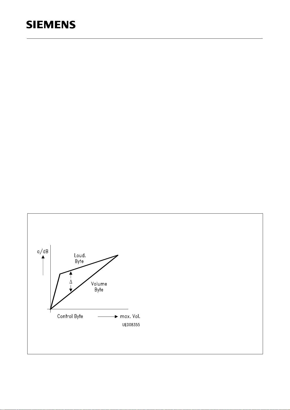
2
C Bus controlled
Loudness function starting at max.
vol. then ∆ continuously increasing.
Figure 3
Semiconductor Group 5 04.96
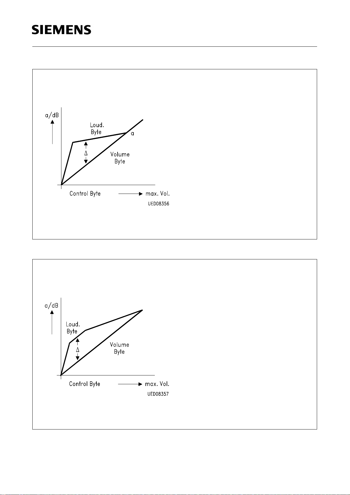
TDA 4350X
Loudness function starting at vol. a
then ∆ continuously increasing.
Figure 4
Loudness function starting at max.
vol. increasing to ∆, following
constant ∆.
Figure 5
Semiconductor Group 6 04.96
TDA 4350X
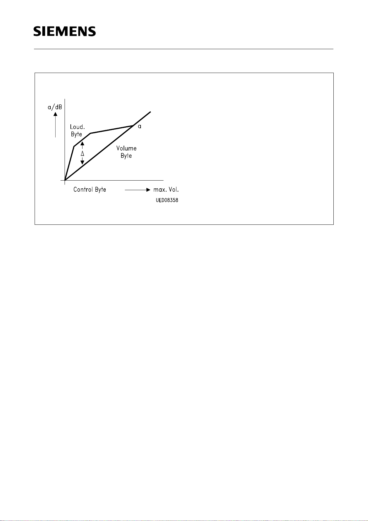
Loudness function starting at vol. a
increasing to ∆, following constant ∆.
Figure 6
3. In the following signalpath there is tone control, consisting of bass and treble control.
Bass control offers a control range of + 16 dB to – 14 dB with a stepwidth of 2 dB.
Frequency characteristic, 1st order or 2nd order (resonance type) is fixed by external
components. Treble control also offers a control range of + 16 dB to – 14 dB with a
stepwidth of 2 dB. The treble control corner frequency is determinated by an external
capacitor.
A second clipping detector allows to detect clipping in tone control part.
4. Last stages in signal path are four strictly independent controllable output attenuators
to realize balance and fader function. Each unit offers a control range of 0 dB to
– 38.75 dB in steps of 1.25 dB. The AF outputs are of a class A-type to avoid
distortion via software, the output fan-out can be increased to drive loads up
to > 1.5 kΩ.
One output of each stereo channel can be inverted software controlled, to drive easily
bridge power amplifiers.
5. Mute control may be either done via the volume control setting, or directly for all
outputs by setting the IM (immediately mute) bit via I
2
C Bus. The second bus
controlled mute mode is mute after signal zero crossing (ZCM). Two zero cross
detectors are built-in, therefore this mute control works independent for left and right
channel. Signal off- and on-switching is performed under zero cross detector control.
The ZCM status can be read out via I
2
C Bus (ZCS). After activating ZCM, the ZCS
(zero crossing status) bit is set to ‘1’, when all outputs are muted after zero crossing.
After deactivating ZCM, the ZCS bit is set to ‘0’ when all outputs are switched on after
zero crossing. The IM mute overwrites ZCM mute. Third mute control is hardware
mute via a mute pin. If the mute pin is switched to ground all outputs are muted
immediately. Hardware mute overwrites all other mute modes.
Semiconductor Group 7 04.96
TDA 4350X
2.2 Controlpart
2
All functions are controlled via an I
The telegram structure is built as follows:
Startcondition – chipaddress – any number of databytes – stopcondition.
For the databytes the following conditions must be fulfilled:
Before transmitting a databyte a subaddress byte must first be placed in the data
telegram.
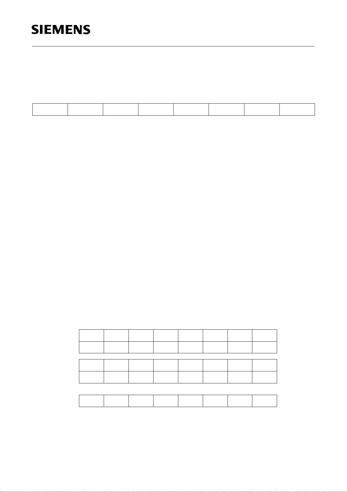
2.2.1 Chipaddress
MSB LSB
1000011R/W
R/W = ‘0’ → Read R/W = ‘1’ → Write
C Bus interface. All data are stored into a latch circuit.
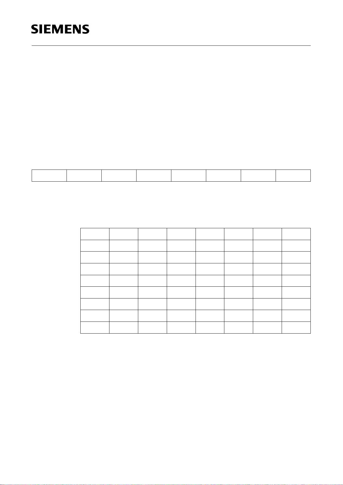
2.2.2 Subaddress Bytes
MSB LSB
Switchbyte 0 0 0 0 0 0 0 0
Inputlevel 0 0 0 0 0 0 0 1
Volume 0 0 0 0 0 0 1 0
Loudness 0 0 0 0 0 0 1 1
Bass/Treble 0 0 0 0 0 1 0 0
Out rear left 0 0 0 0 0 1 0 1
Out front left 0 0 0 0 0 1 1 0
Out rear right 0 0 0 0 0 1 1 1
Out front right 0 0 0 0 1 0 0 0
Semiconductor Group 8 04.96
TDA 4350X
2.2.3 Control Bytes
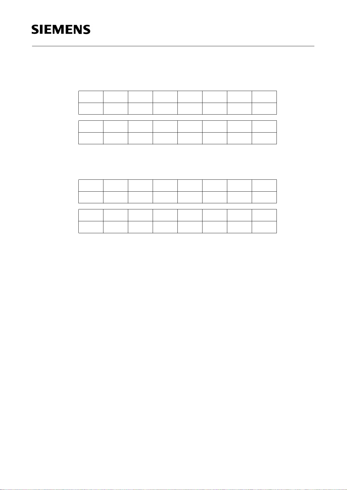
a) Switch Control Byte
MSB LSB
ZCM IM Fan Ph IN-3 IN-2 IN-CD X
IN-CD = ‘0’
IN-CD = ‘1’
IN-2 = ‘0’
IN-2 = ‘1’
IN-3 = ‘0’
IN-3 = ‘1’
CD input OFF; power ON
CD input ON
Input 2 OFF; power ON
Input 2 ON
Input 3 OFF; power ON
Input 3 ON
If no input is selected, mute function is active.
If no protection against multiple selection implemented!
Ph = ‘0’
Ph = ‘1’
Fan = ‘0’
Fan = ‘1’
IM = ‘0’
IM = ‘1’
ZCM = ‘0’
ZCM = ‘1’
Bridgepower amplifier operation ON; power ON
Normal operation
Normal operation; power ON
Increased Fan out ON
Normal operation; power ON
Immediate mute for all AF outputs
Normal operation; power ON
Mute after signal zero crossing
IM overwrites ZCM, handware mute overwrites all other mute modes.
b) Input Level Control Byte
MSB LSB
Min. gain XXXX0000
Min. gain + 1 XXXX0001power ON
Max. gain – 1 XXXX1001
Max. gain XXXX1010
to
Max. gain XXXX1111
Semiconductor Group 9 04.96
TDA 4350X
c) Volume Level Control Byte
MSB LSB
Min. gain X 0000000
Min. gain + 1 X 0000001power ON
Max. gain – 1 X 0111110
Max. gain X 0111111
d) Loudness Control Byte
MSB LSB
Min. gain X Ld 000000
Min. gain + 1 X Ld 000001power ON
Max. gain – 1 X Ld 111110
Max. gain X Ld 111111
Ld = ‘0’ Loudness OFF; power ON
(loudness attenuator has the same setting
as volume attenuator)
Ld = ‘1’ Loudness ON
Semiconductor Group 10 04.96
 Loading...