

Siemens TCA3727G, TCA3727 Datasheet
2-Phase Stepper-Motor Driver
TCA 3727
Overview Bipolar IC
Features
• 2 x 0.75 amp. / 50 V outputs
• Integrated driver, control logic and current control
(chopper)
• Fast free-wheeling diodes
• Max. supply voltage 52 V
• Outputs free of crossover current
• Offset-phase turn-ON of output stages
• Z-diode for logic supply
P-DIP-20-6
• Low standby-current drain
• Full, half, quarter, mini step
P-DSO-24-3
Type Ordering Code Package
TCA 3727 Q67000-A8302 P-DIP-20-6
TCA 3727 G Q67000-A8335 P-DSO-24-3
Description
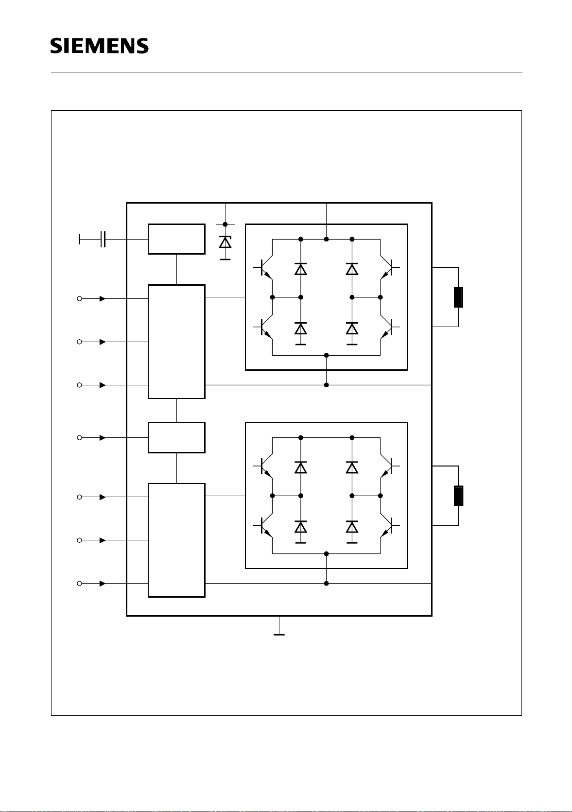
TCA 3727 is a bipolar, monoli thic IC for driving bipolar s tepper motors, DC motors and
other inductive loads that operate on constant current. The control logic and power
output stages for two bipolar windings are integrated on a single chip which permits
switched current control of motors with 0.75 A per phase at operating voltages up to
50 V.
Semiconductor Group 1 1998-02-01

TCA 3727
The direction and value of current are programmed for each phase via separate control
inputs. A common oscillator generates the timing for the current control and turn-on with
phase offset of the two output stages. The two output stages in a full-bridge configuration
have integrated, fast free-wheeling diodes and are free of crossover current. The logic is
supplied either sep arately with 5 V or taken f rom the motor su pply voltage b y way of a
series resistor and an integrated Z-diode. The device can be driven directly by a
microprocessor with the possibility of a ll modes from ful l step through ha lf step to mini
step.
Semiconductor Group 2 1998-02-01
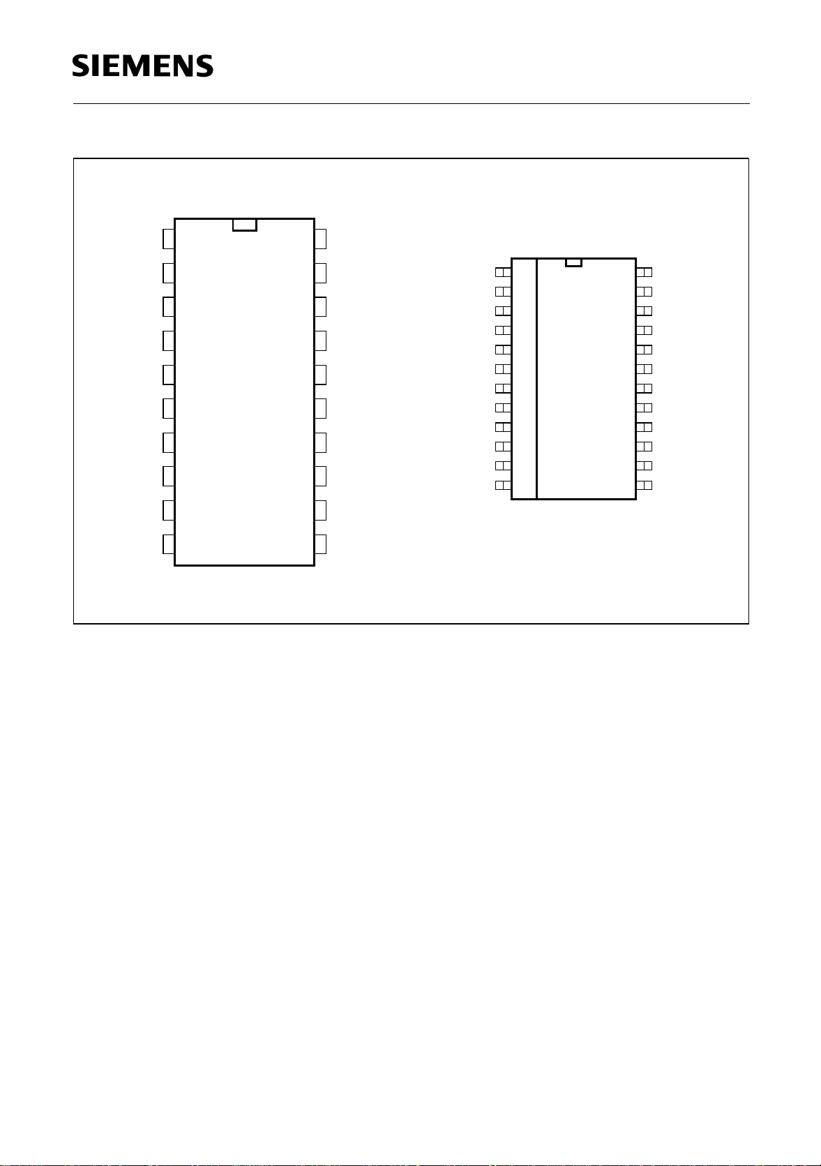
TCA 3727 TCA 3727 G
TCA 3727
1
10
Ι
2
11
Ι
Phase 1
OSC
GND
GND
3
4
5
6
7
8
12
V
9
S
Q12
10
20
19
18
17
16
15
14
13
12
11
IEP00696
Ι
20
21
Ι
Phase 2
Inhibit
GND
GND
Q21Q11
RR
V
L
Q22
Figure 1 Pin Configuration (top view)
10
Ι
Ι
11
Phase 1
OSC
GND
GND
GND
GND
Q11
R
1
++
V
S
Q12
241
232
223
214
205
196
187
178
169
1510
1411
1312
IEP00898
21
Ι
Phase 2
Inhibit
GND
GND
GND
GND
Q21
R
2
V
L
Q22
20
Ι
Semiconductor Group 3 1998-02-01
Pin Definitions and Functions
Pin No. Function
TCA 3727
1, 2, 19, 20
(1, 2, 23, 24)
Digital control inputs IX0, IX1 for the magnitude of the current of
1)
the particular phase.
IX1 IX0 Phase Current Example of
Motor Status
H H 0 No current
H L 1/3
LH 2/3
LL
I
max
I
I
max
max
Hold
Set
Accelerate
typical I
R
= 1 Ω : 750 mA
sense
max
with
3 Input Phase 1; controls the current through phase winding 1. On
H-potential the phase current flows from Q11 to Q12, on L-potential in
the reverse direction.
5, 6, 15, 16
Ground; all pins are connected internally.
(5, 6, 7, 8, 17,
18, 19, 20)
1)
4 Oscillator; works at approx. 25 kHz if this pin is wired to ground
across 2.2 nF.
8 (10)
1)
7, 10 (9, 12)
Resistor R1 for sensing the current in phase 1.
1)
Push-pull outputs Q11, Q12 for phase 1 with integrated
free-wheeling diodes.
9 (11)
1)
Supply voltage; block to ground, as close as possible to the IC, with
a stable electrolytic capacitor of at least 10 µF in parallel with a
ceramic capacitor of 220 nF.
12 (14)
1)
Logic supply voltage; either supply with 5 V or connect to + VS
across a series resistor. A Z-diode of approx. 7 V is integrated. In both
cases block to ground directly on the IC with a stable electr olytic
capacitor of 10 µF in parallel with a ceramic capacitor of 100 nF.
11, 14
(13, 16)
13 (15)
Semiconductor Group 4 1998-02-01
1)
1)
Push-pull outputs Q22, Q21 for phase 2 with integrated free
wheeling diodes.
Resistor R2 for sensing the current in phase 2.

Pin Definitions and Functions (cont’d)
Pin No. Function
17 (21)
1)
Inhibit input; the IC can be put on standby by low potential on this
pin. This reduces the current consumption substantially.
18 (22)
1)
Input phase 2; controls the current flow through phase winding 2. On
H-potenti al the phase cur rent flows fr om Q21 to Q22, on L potential i n
the reverse direction.
1)
TCA 3727 G only
TCA 3727
Semiconductor Group 5 1998-02-01
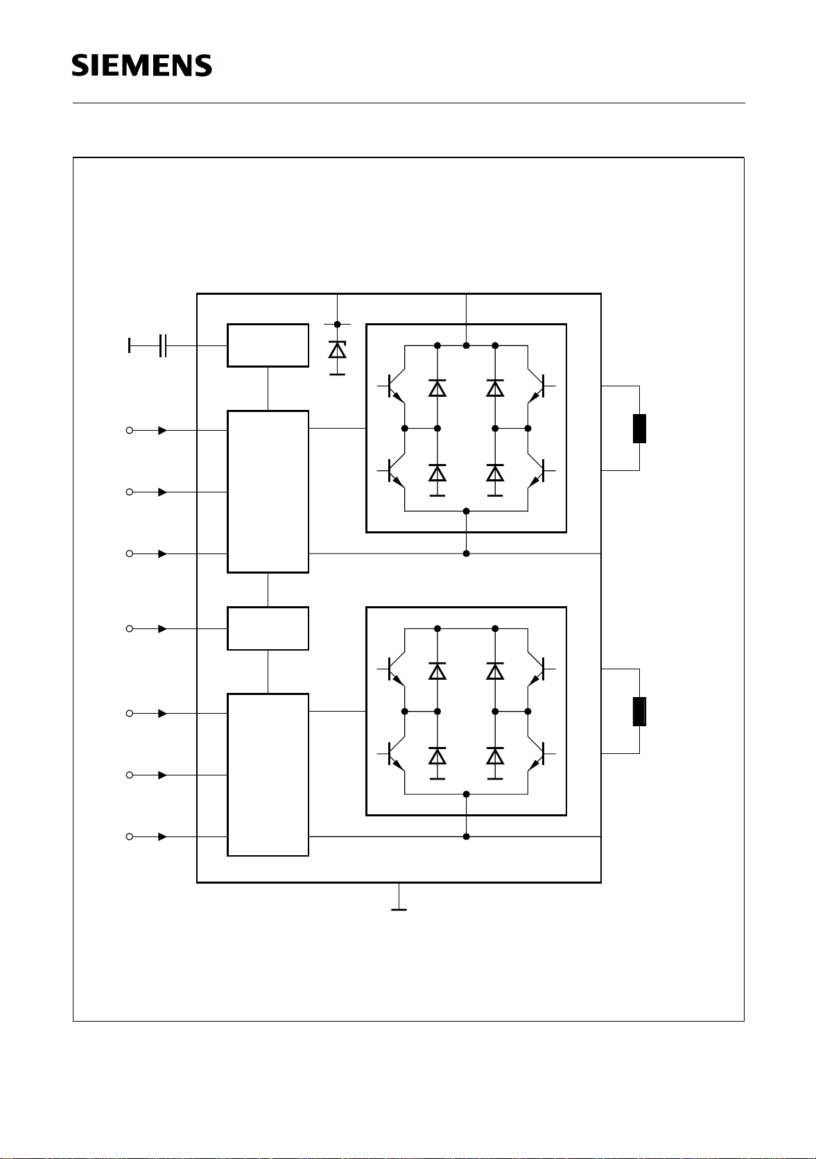
TCA 3727
+
V
LS
12 9
V
+
10
Ι
11Ι
Phase 1
Inhibit
20Ι
4
1
2
3
17
20
OSC
Function
Logic
Phase 1
Inhibit
10
14
7
8
Q11
Q12
R
1
Q21
Phase 1
Phase 2
Q22
21Ι
19
Function
Logic
11
Phase 2
Phase 2
18
13
R
2
5, 6, 15, 16
GND
IEB00697
Figure 2 Block Diagram TCA 3727
Semiconductor Group 6 1998-02-01
TCA 3727
Ι
10
11
Ι
Phase 1
Inhibit
4
1
2
3
21
Oscillator
Functional
Logic
Phase 1
Inhibit
V
+
LS
V
+
14 11
T11
T13
T21
D12D11
T12
D14D13
T14
D21 D22
T22
12
10
16
9
Q11
Q12
R
1
Q21
Phase 1
Ι20
Ι21
24
23
Functional
Logic
Phase 2
Phase 2
22
Figure 3 Block Diagram TCA 3727 G
T23
5-8, 17-19
GND
D23 D24
T24
13
15
IEB00899
Q22
R
2
Phase 2
Semiconductor Group 7 1998-02-01
Absolute Maximum Ratings
T
= – 40 to 125 °C
A
Parameter Symbol Limit Values Unit Remarks
min. max.
TCA 3727
Supply voltage
Logic supply voltage
Z-current of
V
L
Output current
Ground current
Logic inputs
R
, R2, oscillator input voltage V
1
Junction temperature
Storage temperature
V
V
I
L
I
Q
I
GND
V
V
T
T
T
S
L
Ixx
RX,
OSC
j
j
stg
052 V–
0 6.5 V Z-diode
–50 mA–
– 1 1 A –
– 2 2 A –
– 6 VL + 0.3 V IXX; Phase 1, 2; Inhibit
– 0.3 VL + 0.3 V –
–
–
125
150
°C°C–
max. 1,000 h
– 50 125 °C–
Semiconductor Group 8 1998-02-01
Operating Range
Parameter Symbol Limit Values Unit Remarks
min. max.
TCA 3727
Supply voltage
Logic supply voltage
Case temperature
Output current
Logic inputs
Thermal Resistances
Junction ambient
Junction ambient
(soldered on a 35 µm thick 20 cm
PC board copper area)
Junction case
V
V
S
L
550V–
4.5 6.5 V without series
resistor
T
I
V
C
Q
IXX
– 40 110 °C measured on pin 5
P
= 2 W
diss
– 1000 1000 mA –
– 5 V
V IXX; Phase 1, 2;
L
Inhibit
R
th ja
R
th ja
2
R
th jc
–
–
–
56
40
18
K/W
K/W
K/W
P-DIP-20-3
P-DIP-20-3
measured on pin 5
P-DIP-20-3
Junction ambient
Junction ambient
(soldered on a 35 µm thick 20 cm
PC board copper area)
Junction case
R
th ja
R
th ja
2
R
th jc
–
–
–
75
50
15
K/W
K/W
K/W
P-DSO-24-3
P-DSO-24-3
measured on pin 5
P-DSO-24-3
Semiconductor Group 9 1998-02-01
 Loading...