

Siemens SMBT3904S Datasheet
SMBT 3904S
Semiconductor Group
Sep-07-19981
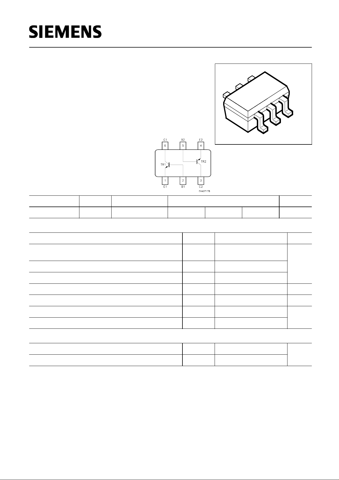
NPN Silicon Switching Transistor Array
• High DC current gain: 0.1mA to 100mA
• Low collector-emitter saturation voltage
• Two ( galvanic) internal isolated Transistors
with high matching in one package
• Complementary type: SMBT 3906S (PNP)
VPS05604
6
3
1
5
4
2
Type Marking Ordering Code PackagePin Configuration
1/4=E1/E2s1ASMBT 3904S 2/5=B1/B2 3/6=C2/C1 SOT-363Q62702-A1201
Maximum Ratings
UnitParameter Symbol Value
Collector-emitter voltage
V
CEO
V40
60Collector-base voltage
V
CBO
Emitter-base voltage 6
V
EBO
DC collector current
I
C
mA200
250 mW
Total power dissipation,
T
S
= 115 °C
P
tot
°C
T
j
Junction temperature 150
Storage temperature
T
st
g
- 65...+150
Thermal Resistance
Junction ambient
1)
R
thJA
≤275
K/W
Junction - soldering point
R
thJS
≤140
1) Package mounted on pcb 40mm x 40mm x 1.5mm / 0.5cm2 Cu
Semiconductor Group 1 1998-11-01
SMBT 3904S
Semiconductor Group
Sep-07-19982
Electrical Characteristics at
T
A
=25°C, unless otherwise specified.
Parameter Symbol UnitValues
typ. max.min.
DC Characteristics
Collector-emitter breakdown voltage
I
C
= 1 mA,
I
B
= 0
V
(BR)CEO
V40 - -
Collector-base breakdown voltage
I
C
= 10 µA,
I
B
= 0
V
(BR)CBO
60 - -
V
(BR)EBO
- -6Emitter-base breakdown voltage
I
E
= 10 µA,
I
C
= 0
Collector cutoff current
V
CB
= 30 V,
I
E
= 0
nA
I
CBO
- - 50
DC current gain 1)
I
C
= 100 µA,
V
CE
= 1 V
I
C
= 1 mA,
V
CE
= 1 V
I
C
= 10 mA,
V
CE
= 1 V
I
C
= 50 mA,
V
CE
= 1 V
I
C
= 100 mA,
V
CE
= 1 V
h
FE
40
70
100
60
30
-
-
-
-
-
-
-
300
-
-
-
Collector-emitter saturation voltage1)
I
C
= 10 mA,
I
B
= 1 mA
I
C
= 50 mA,
I
B
= 5 mA
V
CEsat
-
-
-
-
0.2
0.3
V
Base-emitter saturation voltage 1)
I
C
= 10 mA,
I
B
= 1 mA
I
C
= 50 mA,
I
B
= 5 mA
V
BEsat
0.65
-
-
-
0.85
0.95
1) Pulse test: t < 300µs; D < 2%
Semiconductor Group 2 1998-11-01
SMBT 3904S
Semiconductor Group
Sep-07-19983
Electrical Characteristics at
T
A
= 25°C, unless otherwise specified.
Parameter ValuesSymbol Unit
max.typ.min.
AC Characteristics
f
T
300 - MHz-Transition frequency
I
C
= 10 mA,
V
CE
= 20 V, f = 100 MHz
C
cb
- -Collector-base capacitance
V
CB
= 5 V, f = 1 MHz
pF4
C
eb
- - 8Emitter-base capacitance
V
EB
= 0.5 V, f = 1 MHz
h
11e
1 10-Short-circuit input impedance
I
C
= 1 mA,
V
CE
= 10 V, f = 1 kHz
kΩ
h
12e
0.5 8 10
-4
-Open-circuit reverse voltage transfer ratio
I
C
= 1 mA,
V
CE
= 10 V, f = 1 kHz
h
21e
100 -Short-circuit forward current transfer ratio
I
C
= 1 mA,
V
CE
= 10 V, f = 1 kHz
-400
h
22e
1 - 40
µs
Open-circuit output admittance
I
C
= 1 mA,
V
CE
= 10 V, f = 1 kHz
Noise figure
I
C
= 100 µA,
V
CE
= 5 V,
R
S
= 1 kΩ,
f
= 1 kHz, ∆ f = 200 Hz
F
- - 5 dB
Delay time
V
CC
= 3 V,
I
C
= 10 mA,
I
B1
= 1 mA,
V
BE(off)
= 0.5 V
t
d
- - 35 ns
Rise time
V
CC
= 3 V,
I
C
= 10 mA,
I
B1
= 1 mA,
V
BE(off)
= 0.5 V
t
r
- - 35
Storage time
V
CC
= 3 V,
I
C
= 10 mA,
I
B1
=
I
B2
= 1mA
t
stg
- - 200
Fall time
V
CC
= 3 V,
I
C
= 10 mA,
I
B1
=
I
B2 =
1mA
t
f
- - 50
Semiconductor Group 3 1998-11-01
 Loading...