

Siemens SMBT2222A, SMBT2222 Datasheet
NPN Silicon Switching Transistors SMBT 2222
SMBT 2222 A
● High DC current gain: 0.1 mA to 500 mA
● Low collector-emitter saturation voltage
● Complementary types: SMBT 2907,
SMBT 2907 A (PNP)
Type Ordering Code
SMBT 2222
SMBT 2222 A
Marking
s1B
s1P
(tape and reel)
Q68000-A6481
Q68000-A6473
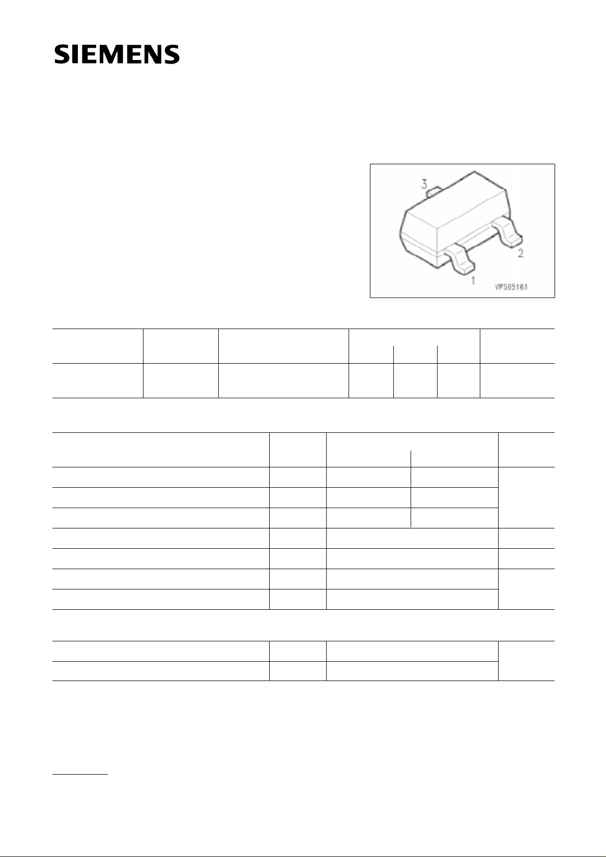
Pin Configuration
1 2 3
B E C
Package
SOT-23
Maximum Ratings
Parameter Symbol Values Unit
SMBT 2222 SMBT 2222 A
Collector-emitter voltage V
Collector-base voltage VCB0
Emitter-base voltage V
Collector current IC mA
Total power dissipation, T
S = 77 ˚C Ptot mW
Junction temperature Tj ˚C
Storage temperature range T
CE0 V
30 40
60 75
EB0
56
600
330
150
stg
– 65 … + 150
Thermal Resistance
1)
Junction - ambient
2)
Rth JA ≤ 290 K/W
Junction - soldering point Rth JS ≤ 220
1)
For detailed information see chapter Package Outlines.
2)
Package mounted on epoxy pcb 40 mm × 40 mm × 1.5 mm/6 cm2 Cu.
Semiconductor Group 1
5.91
Electrical Characteristics
I
I
I
I
I
I
I
I
I
I
I
I
I
I
A = 25 ˚C, unless otherwise specified.
at T
DC characteristics
SMBT 2222
SMBT 2222 A
UnitValuesParameter Symbol
min. typ. max.
(BR)CE0
V
C = 10 mA SMBT 2222
SMBT 2222 A
Collector-base breakdown voltage
C = 10 µA SMBT 2222
SMBT 2222 A
Emitter-base breakdown voltage
E = 10 µA SMBT 2222
SMBT 2222 A
Collector cutoff current
(BR)CB0
V
(BR)EB0
V
I
CB0
VCB = 50 V SMBT 2222
CB = 60 V SMBT 2222 A
V
CB = 50 V, TA = 150 ˚C SMBT 2222
V
CB = 60 V, TA = 150 ˚C SMBT 2222 A
V
EB = 3 V
V
C = 100 µA, VCE = 10 V
C = 1 mA, VCE = 10 V
C = 10 mA, VCE = 10 V
C = 150 mA, VCE = 1 V
C = 150 mA, VCE = 10 V
C = 500 mA, VCE = 10 V
1)
1)
1)
1)
SMBT 2222
SMBT 2222 A
C = 10 mA, VCE = 10 V,
A = 55 ˚C SMBT 2222 A
T
Collector-emitter saturation voltage
C = 150 mA, IB = 15 mA SMBT 2222
1)
SMBT 2222 A
C = 500 mA, IB = 50 mA SMBT 2222
I
EB0 ––10
h
FE
SMBT 2222 A
Base-emitter saturation voltage
C = 150 mA, IB = 15 mA SMBT 2222
C = 500 mA, IB = 50 mA SMBT 2222
1)
SMBT 2222 A
VBEsat
SMBT 2222 A
30
40
60
75
5
6
–
–
–
–
35
50
75
50
100
30
40
35
–
–
–
–
–
0.6
–
–
–
–
–
–
–
–
–
–
–
–
–
–
–
–
–
–
–
–
–
–
–
–
–
–
–
–
–
–
–
–
–
–
10
10
10
10
–
–
–
–
300
–
–
–
0.4
0.3
1.6
1.0
1.3
1.2
2.6
2.0
VCollector-emitter breakdown voltage
nA
nA
µA
µA
nAEmitter cutoff current
–DC current gain
VVCEsat
1)
Pulse test conditions: t ≤ 300 µs, D = 2 %.
Semiconductor Group 2
 Loading...