

Siemens SLx 24C64 Technical data
查询SLE 24C64供应商
Standard EEPROM ICs
SLx 24C64
64 Kbit (8192 × 8 bit)
Serial CMOS-EEPROM with
2
C Synchronous 2-Wire Bus
I
Data Sheet 1999-02-02

Edition 1999-02-02
Published by Siemens AG,
Bereich Halbleite r , Ma rk eting-
Kommunikation, Balanstraße 73,
81541 München
©
Siemens AG 1999.
All Rights Reserved.
Attention please!
As far as patents or other rights of third parties are concerned, liability is only assumed
for components, not for applications, processes and circuits implemented within
components or assemblies.
The information describes the type of
component and shall not be considered as
assured characteristics.
Terms of delivery and rights to change design
reserved.
For questions on technology, delivery and
prices please contact the Semiconductor
Group Offices in Germany or the Siemens
Companies and Representatives worldwide
(see address list).
Due to technical requirements components
may contain dangerous substances. F or
information on the types in question please
contact your nearest Siemens Office,
Semiconductor Group.
Siemens AG is an approved CECC
manufacturer.
Packing
Please use the recycling operators known to
you. We can also help you – get in touch with
your nearest sales office. By agreement we
will take packing material back, if it is sorted.
You must bear the costs of transport.
For packing material that is returned to us
unsorted or which we are not obliged to
accept, we shall have to invoice you for any
costs incu rred.
Components used in life-support devices
or systems must be expressly authorized
for such purpose!
1
Critical components
Group of Siemens AG, may only be used in
life-support devices or systems
of the Semiconductor
2
with the
express written approval of the
Semiconductor Group of Siemens AG.
1 A critical component is a component used
in a life-support device or system whose
failure can reasonably be expected to
cause the failure of that life-support
device or system, or to affect its safety or
effectiveness of that device or system .
2 Life support devices or systems are
intended (a) to be implanted in the human
body, or (b) to support and/or maintain
and sustain human life. If they fail, it is
reasonable to assume that the health of
the user may be endangered.
SLx 24C64
Revision History: Current Version: 1999-02-02
Previous Version: 05.98, 07.98
Page
(in previous
Version)
Changes in the complete
Page
(in current
Version)
Subjects (major changes since last revision)
P-DIP-8-4 changed to P-DIP-8-3, P-DSO-8-3 changed to P-DSO-8-2.
document
34Text was changed to “Typical programming time 5 ms for up to
32 bytes”.
4 5 SLA 24C64-D-3, SLA 24C64-D-3/P, SLA 24C64-S-3
and SLA 24C64-S-3/P deleted.
4 5 Voltage changed from 4.5 V...5.5 V to 2.7 V...5.5 V.
4 5 Text “3 V types with automotive temperature range
(– 40 °C … + 125 °C)” deleted.
4 5 Package (TSSOP, die, wafer delivery) added.
6 7 Footnote added “Values are temperature ….”
6 7 Text changed to “The device with a voltage range of 2.7 … 5.5. V is
available …”.
11, 12 13, 15 The erase/write cycle is finished latest after 10
8ms.
14 15 Text added “(see figure 10)”.
18 19 Figure 13: “CSW” changed to “CSR”.
21 23 The write or erase cycle is finished latest after 10
4ms.
22 24 Line “Supply voltage”: Text deleted.
23 24 Supply current (write) 3 mA
1 mA.
23 24 Line added “Supply current (read)”.
24 26 The line “erase/write cycle” removed.
24 26 Chapter 8.4 “Erase and Write Characteristics” added.
Page Protection Mode™ is a trademark of Siemens AG.
2
C Bus
I
Purchase of Siemens I
2
C system provided the system co nf orm s to the I2C specifications defined by Philips.
the I
2
C components conveys the license under the Philips I2C patent to use the components in
64 Kbit (8192 × 8 bit) Serial CMOS
2
EEPROMs, I
Preliminary
1Overview
1.1 Features
• Data EEPROM internally organized as
8192 bytes and 256 pages × 32 bytes
• Page Protection Mode for protecting the
EEPROM against unintended data changes
(SLx 24C64.../P types only)
• Low power CMOS
V
•
• Two wire serial interface bus, I
= 2.7 to 5.5 V operation
CC
C Synchronous 2-Wire Bus
2
C-Bus compatible
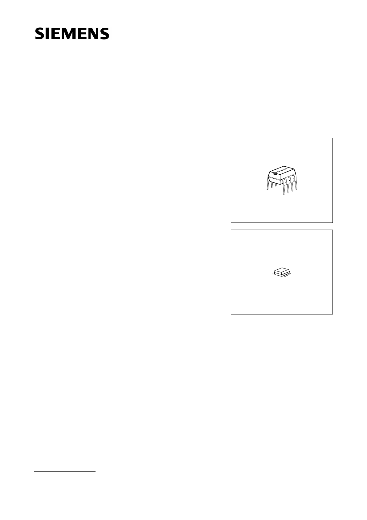
SLx 24C64
P-DIP-8-3
• Three chip select pins to address 8 devices
• Filtered inputs for noise suppression with
Schmitt trigger
• Clock frequency up to 400 kHz
• High prog ramming flexibi lity
– Internal programming voltage
– Self timed programming cycle including erase
– Byte-write and page-wr ite programming, between
1 and 32 bytes
– Typical programming time 5 ms for up to 32 bytes
• High reliabil ity
6
– Endurance 10
cycles
– Data retention 40 years
1)
1)
– ESD protection 4000 V on all pins
• 8 pin DIP/DSO packages
• Available for extended temperature ranges
– Industrial: − 40 °C to + 85 °C
– Automotive: − 40 °C to + 125 °C
P-DSO-8-2
1)
Values are temperature de pendent, for further information please refer to your Siemens sales offi ce .
Semiconductor Group 4 1999-02-02
SLx 24C64
Ordering Information
Type Ordering Code Package Temperature Voltage
SLA 24C64-D
SLA 24C64-D/P
SLA 24C64-S
SLA 24C64-S/P
SLE 24C64-D
SLE 24C64-D/P
SLE 24C64-S
SLE 24C64-S/P
Q67100-H3768
Q67100-H3762
Q67100-H3767
Q67100-H3761
Q67100-H3238
Q67100-H3758
Q67100-H3239
Q67100-H3757
Other types are available on request:
– Temperature range (– 55 °C … + 150 °C)
– Package (TSSOP, die, wafer delivery)
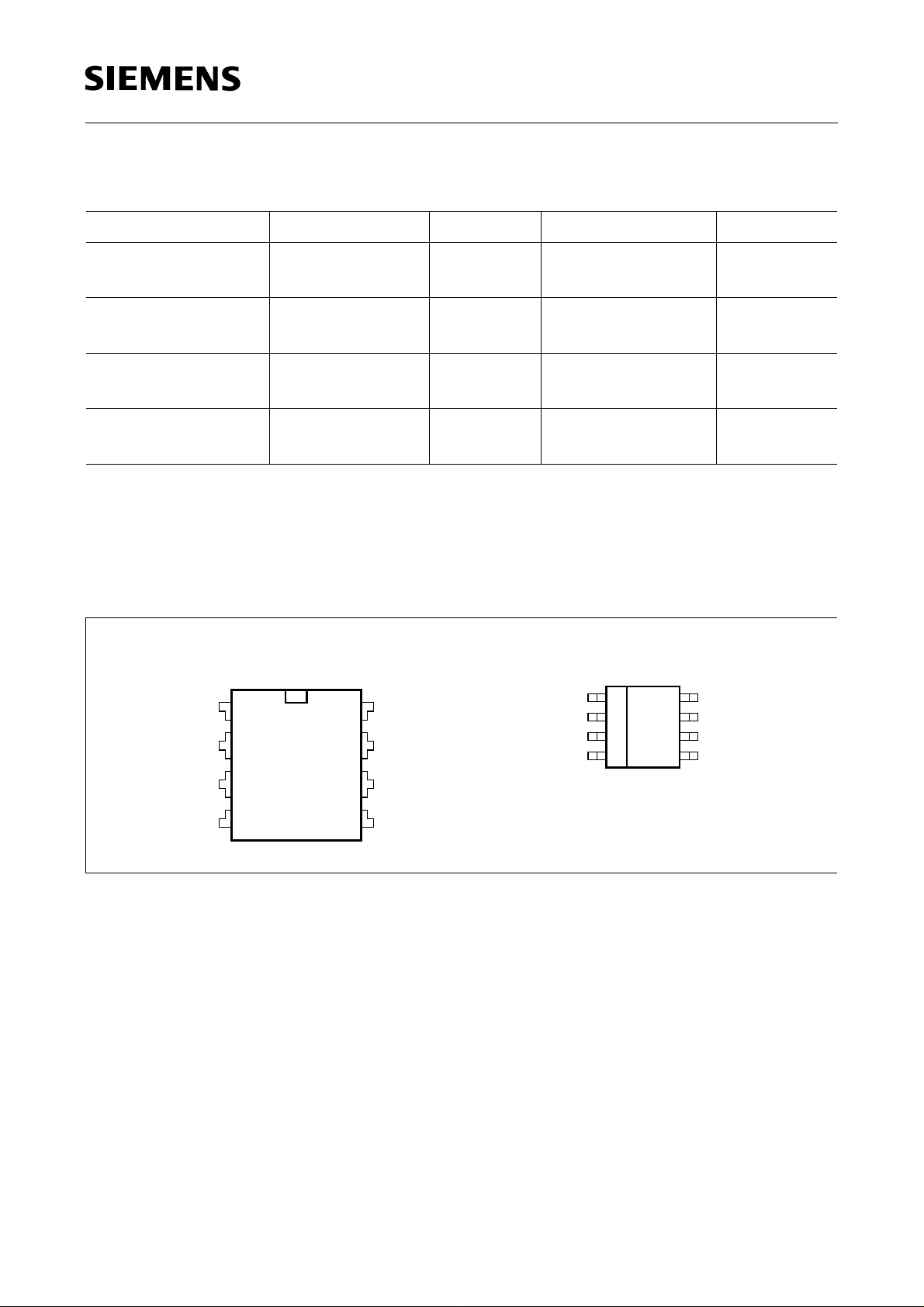
1.2 Pin Configuration
CS0
CS1
CS2
18
V
CC
WP
72
SCL63
P-DIP-8-3 – 40 °C … + 85 °C 2.7 V...5.5 V
P-DSO-8-2 – 40 °C … + 85 °C 2.7 V...5.5 V
P-DIP-8-3 – 40°C … + 125 °C 2.7 V...5.5 V
P-DSO-8-2 – 40°C … + 125 °C 2.7 V...5.5 V
P-DSO-8-2P-DIP-8-3
CS0
CS1
CS2
V
SS
1
2
3
4
IEP02124
V
8
CC
7
WP
6
SCL
SDA
5
V
SS
IEP02125
SDA54
Figure 1
Pin Configuration (top view)
Semiconductor Group 5 1999-02-02
Pin Definitions and Functions
Table 1
Pin No. Symbol Function
1, 2, 3 CS0, CS1, CS2 Chip select inputs
SLx 24C64
4
V
SS
Ground
5 SDA Serial bidirectional data bus
6 SCL Serial clock input
7 WP Write protection input
8
V
CC
Supply voltage
Pin Description
Serial Clock (SCL)
The SCL input is used to clock data into the device on the rising edge and to clock data
out of the device on the falling edge.
Serial Data (SDA)
SDA is a bidirectional pin used to transfer addresses, data or control information into the
device or to transfer data out of the device. The output is open drain, performing a wired
AND function with any number of other ope n drain or open col lector device s. The SDA
V
bus requires a pull-up resistor to
CC
.
Chip Select (CS0, CS1, CS2)
The CS0, CS1 and CS2 pins are chip sele ct inputs eithe r hard wired o r actively driv en
V
to
or VSS. These inputs allow the se lection of one of eight p ossible devic es sharing
CC
a common bus.
Write Protection (WP)
V
WP switched to
WP switched to
Semiconductor Group 6 1999-02-02
allows normal read/write operations.
SS
V
protects the EEPROM against changes (hardware write protection).
CC
SLx 24C64
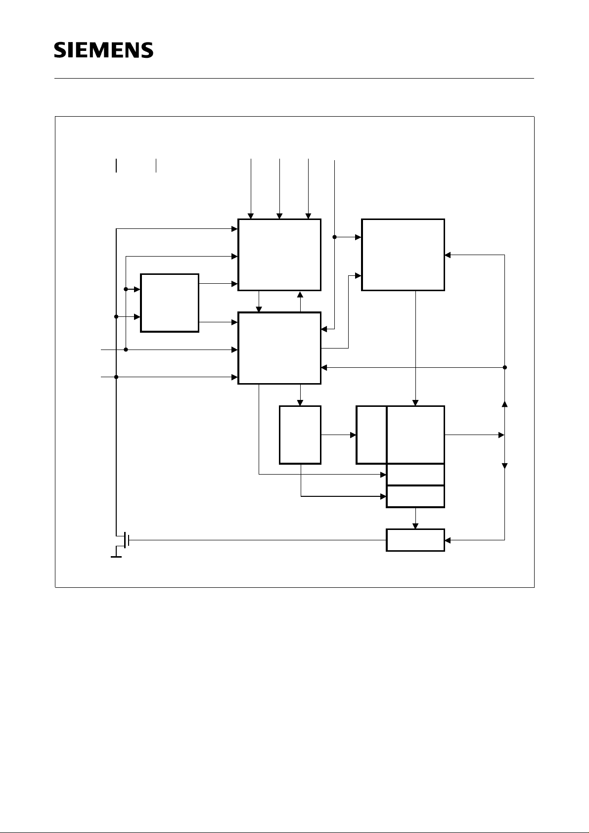
2 Description
The SLx 24C64 device is a serial electrically erasable and programmable read only
memory (EEPROM), organized as 8192 × 8 bit. The data memory is divided into
256 pages. The 32 bytes of a page can be programmed simultaneously.
2
The device conforms to th e spe cifica tion of th e 2-wi re seria l I
2
pins allow the addressing of 8 devices on the I
C-Bus. Low voltage design permits
operation down to 2.7 V with low active and standby currents. All devices have a
6
minimum endurance of 10
erase/write cycles1).
The device operates at 5.0 V ± 10% with a maximum clock frequency of 400 kHz and at
2.7 ... 5.5 V with a maximum clock frequency of 100 kHz. The device with a voltage
range of 2.7 … 5.5. V is available in two temperature ranges for industrial and
automotive applications. The EEPROMs are mounted in eight-pin DIP and DSO
packages or are also supplied as chips.
C-Bus. Three chip select
1)
Values are temperature de pendent, for further information please refer to your Siemens Sales offic e.
Semiconductor Group 7 1999-02-02
SLx 24C64
SCL
SDA
V
SS
V
CC
Start/
Stop
Logic
CS0 CS1 CS2
Chip Address
Control
Logic
Serial
Control
Logic
Address
Logic
WP
Programming
Control
H.V. Pump
X
DEC
EEPROM
Figure 2
Block Diagram
Page Logic
Y DEC
Dout/ACK
IEB02525
Semiconductor Group 8 1999-02-02
SLx 24C64
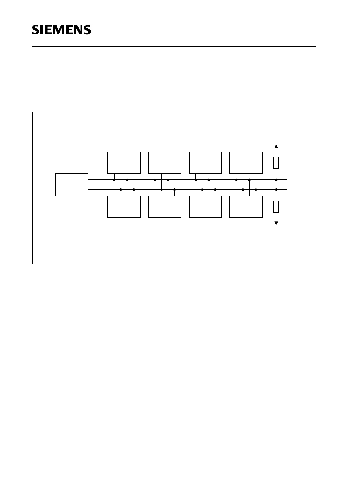
3 I2C-Bus Characteristics
2
Access to the SLx 24C64 device is given via the I
of two wires SCL and SDA for clock and data. The protocol is master/slave oriented,
where the serial EEPROM always takes the role of a slave.
Slave 1 Slave 2 Slave 3 Slave 4
SCL
Master
SDA
C bus. This bidirectional bus consists
V
CC
Slave 8Slave 5 Slave 6 Slave 7
V
CC
IES02183
Figure 3
Bus Configuration
Master Device that initiates the transfer of data and provides the clock for transmit
and receive operations.
Slave Device addressed by the master, capable of receiving and transmit ting
data.
Transmitter The device using the SD A as ou tput is defined as the transmi tter. Du e to
the open drain characteristic of the SDA output the device applying a low
level wins.
Receiver The device using the SDA as input is defined as the receiver.
Semiconductor Group 9 1999-02-02
 Loading...