

Siemens SlMATlC S5-010W Operating Instructions Manual
SIEMENS
Programmable Controller
S5-010W
Manual
Order No.: 6ES5 998-OCA21
Issue 1
lnstructions
Contents
Instructions
Programming Instructions
Programming lnstructions
Order No.:
GWA 4NEB 807 1021 -02
GWA4NEB 807 1071-02
SIEMENS
AKTIENGESELLSCHAFT
SIMATIC S5-O10W
Programmable
Controller
Operating
Instructions
SIEMENS
SlMATlC
S5-010W
Programmable Controller
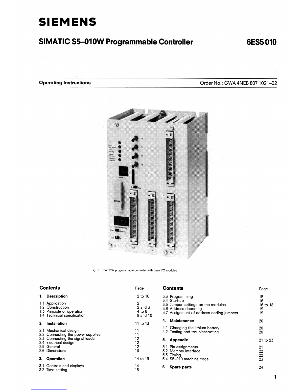
Operating Instructions
Order
No.:
GWA
4NEB
807 1021-02
Fig. 1 S501OW programmable controller with three 110 modules
Contents
Page
Contents
Page
1.
Description
3.3 Programming
3.4 Start-up
3.5 Jumper settings on the modules
3.6 Address decoding
3.7 Assignment of address coding jumpers
1.1 Application
1.2 Construction
1.3 Principle of operation
1.4 Technical specification
2
2 and 3
4 to
8
9
and 10
4.
Maintenance
2.
Installation
4.1 Changing the lithium battery
4.2 Testing and troubleshooting
2.1 Mechanical design
2.2 Connecting the power supplies
2.3 Connecting the signal leads
2.4 Electrical design
2.5 General
2.6
Dimensions
5.
Appendix
5.1 Pin assignments
5.2 Memory interface
5.3 Timing
5.4
S5-010 machine code
3.
Operation
3.1 Controls and displays
3.2 Time setting
6.
Spare parts
1.
Description
1.1
Application
1.2
Construction
1
.l
Application
The S5-010W programmable controller belongs to the-SIMATIC S5
family of programmable controllers and has been designed for use
with small machine tools and adaptive control systems. It is suitable
for automation tasks for which contactors, relays or simple hardwired electronic systems have been used in the past. The range of
functions available permits the assembly of binary logic control
systems with memory and time functions.
Signal input Processing Signal output
24
V
DC
Fig. 2 Application of SWlOW programmable controllers
,
Mech. sensor,
,\e.g. pushbutton,
pressure switch, temperature sensor
Inductive sensor
-1
zny0itive
other
SlMATlC controls
1.2
Construction
SlMATlC S5
S5-010W
PC
I+-$
valves
3
@
Alarm
indicators
other
SlMATlC controls
The S5-010W programmable controller comprises a housing containing plug-in printed-circuit boards measuring 160
X
250 mm.
Each PCB represents a functional unit.
k
1
The modules are housed in an open frame and are interconnected
through a 20-way bus which is secured to the rear of the housing.
The housing frame permits easy mounting in electronic equipment
cabinets and machine tools; no fan is needed.
There are three types of housing available, on with four, one with six
and one with eight module locations.
Central processing unit
900
The CPU contains the following:
Bit processor
Power supply unit,
24
V
primary15 V secondary
Memory for flag operations
Backup battery for retentive flags
Service panel
Receptacle for memory submodule
910
Memory submodule
910
Erasable read-only memory (EPROM) for 1
K,
2K
or
4K
statements,
depending on the version.
Inputltimer module 400
Digital output module 410 (solid-state)
Interface module
772
For interfacing S5-010W programmable controllers to higher-level
control systems.
Programming unit interface module
500
For on-line operation of the S5-010W with the 630, 631 and 670
programming
units.
Mechanical
des~gn as for S5-110 A modules.
Flg 3 S5-010W programmable controllers wlth
4,
6
and 8 module
locations
2
1.
Description
1.2
Construction
S5-010W
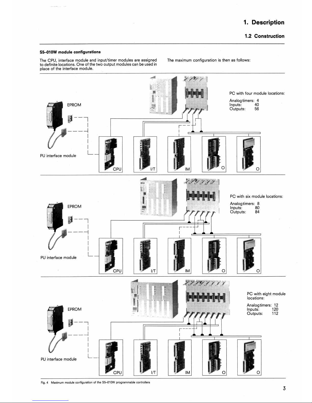
module configurations
The CPU, interface module and inputltimer modules are assigned
The maximum configuration is then as follows:
to definite locations. One of the two output modules can be used in
place of the interface module.
PC with four module locations:
Analog timers: 4
Inputs: 40
Outputs:
56
EPROM
($--l
--p
4
I
I
I
PU interface module
L
PC with six module locations
EPROM
Analogtimers
8
Outputs 84
I#--1
---
i
l
I
I
PU interface module
L
EPROM
I#--1
PC with six module locations.
Analogtimers
8
--
Inputs:
80
Outputs: 84
l
I
I
PU interface module
L
EPROM
(3-7
---
4
l
l
I
L-
PU interface module
l
PC with etght module
locat~ons
Analogtimers 12
Inputs. 120
Outputs 112
Fig. 4 Maximum module configuration of the
S55lOW
programmable controllers
3
1.
Description
1.3
Principle of operation
The program memory contains the STEP 5 program written by the
user. The memory is organized bytewise, one byte comprising
8
bits
and
2
bytes constituting a complete statement, e.g. A1 5.1. This
statement implies the following:
-Examine input 15.1 to see whether it is
"1
"
and AND this signal
with the result of the previous scanning operation.
The statements contained in the program memory are executed
consecutively and cyclically by the processor. The individual memory locations are referenced by an address counter. By
increment-
ing the address counter by
+l,
it
is possible to read out the next
two bytes (a complete statement).
The following is a description of the principle of operation of the PC
by way of example of the
A1 5.1 and = Q 5.3 statements (see Fig. 5).
When the address counter of the processor reaches the appropri-
ate memory location, the "AI 5.1" statement stored there is read
out.
The parameter 5.1 is output via the address bus to all
I10 modules,
where it is decoded by the address decoders.
The operation decoder of the CPU evaluates the operand "I" and
holds all output modules disabled via the enabling bus.
In conjunction with the full parameter, therefore, input 5.1 is
specified and can be examined.
?pending on the signal status at
the input of this element, either
1"
or
"0"
is transmitted on the
input data bus
(DIN) to the sequence logic unit of the processor for
further processing.
From the bit pattern for the letter "A" in the operation
"AI" (A
=
AND), the decoder recognizes that the result of the scan has to be
ANDed with the result of the previous scanning operation in the
logic unit.
The new RLO (result of logic operation) is stored in the logic unit.
The next statement, in this case
"=
Q5.3", is read out by incre-
menting the address counter again. The address 5.3 is output via
the address bus to all
I10 modules, where it is decoded.
The decoder evaluates the operand
"=
Q"
and places the result of
the logic operation
(RLO)
stored in the logic on the output data bus
(DouT). After enabling of the I10 modules, the RLO is available at
output Q5.3. Due to the cyclic execution of the statements, the
output statuses must be stored on the output module.
Program memory
(EPROM)
Address counter
11000 8 00100000101
Statement
r,2e
=Q
5
3
1
i
Operation
I
Dour
11
1
DIN
F
T
l
7
T-\
I
Input 15.1 Output Q5.3
Fig.
5
Principle of operation of the
S5OlOW
programmable controller
1.
Description
1.3
Principle
of
operation
Central processing unit 6ES5900-OAA12
The CPU incorporates the following functional units:
-
Power supply
-
Processor with cycle time monitor
-
Memory for flag operations
-
Receptacle for EPROM submodule
Power supply
The 24 V DC power supply is provided by a non-stabilized power
supply.
The operating voltage of + 5 V required for internal signal processing is produced from the 24
V
supply.
Processor
The processor decodes the programmed statements and executes
the relevant operations (see STEP5 operation set for the S5-010
PC). The execution time for a statement corresponds to the period
of the system clocking and is approximately 20 ys. For 1
K
state-
ments, therefore, this gives a cycle time of 20 ms.
For cycle time monitoring, the program controller contains a 200 ms
timer which is continuously reset by the
"BE"/"BEC" (block end)
and AFO.O (interrupt) operations. If no resetting of the timer takes
place during a 200
rns period, the control system is in an undefined
state. The "Cycle fault" display lights up and the
link between pins
X3
and
X4
via the "Watchdog monitor" relay contact is interrupted.
To prevent the indefinite state of the control system from being
transferred to the machine being controlled it is advisable to run the
+24
V
supply for all output modules through a contactor driven by
the watchdog monitor relay (see Connection diagram, page 11).
This will ensure that all outputs assume the logic state
"0" during a
scan fault.
Memory for flag operations
A 1024 X 1 bit static RAM is used for flag operations. The memory
is subdivided into three areas (see Fig.
7).
Retentive flags:
These flags are addressed by the operations SF, RF,
=
F, etc. The
flag area has battery backup,
i.
e. the flags retain their signal
statuses in the event of power failure. The battery backup can be
disabled by a switch on the CPU (see "Service panel").
Non-retentive flags:
These flags are addressed by the operations SF, RF,
=
F, etc. In the
event of a power failure, this flag area is erased.
Output flags:
Output flags are addressed by output operations (SQ, RQ,
=
Q),
i.
e. they are set and reset in parallel with the outputs. When
scanning the outputs (AQ, ANQ, OQ, ONQ), only these flags are
examined; the actual outputs of output and timer modules cannot
be scanned. Output flags are erased in the event of power failure.
Output flag
000.0 cannot be used; flag FOO.O is only needed for
interrupt processing.
EPROM submodule 910
EPROMs mounted on a plug-in submodule are used to store the
STEP5 program. Submodules are available for
IK,
2K and
4K
statements.
The memory submodule is plugged into the appropriate receptacle
on the programming unit for programming. After programming, the
module is plugged into the receptacle provided for it on the CPU.
Online
~
i
Oif-
line
Processor
256
flags
1
;do.,te",e)
I
,
Fig. 6 Block diagram
of
the CPU
Memory
locatlon Address dec. I hex.
F1F
7
51
1 flags
(retentive)
256
flags
(non-retentive)
255
output flags
(non-retentive)
Q00.1
Fig. 7 Memory
organization,
address assignment

1.
Description
1.3
Principle of operation
Inputltimer module
6ES5400-OAAI
1
The module contains the following:
40 inputs for 24
V
DC
Four of these can be used as interrupt inputs. Interrupts can be
initiated by either the leading edge or trailing edge of the input
signal and can be disabled by removing a jumper.
Four analog timers:
Time ranges: 10 ms
-
100 ms
looms- 1 s
Is -10s
10s
-
100s
Time setting:
Coarse setting by thumbwheel switch
Fine adjustment by built-in potentiometers
Displays:
LEDs light up while the timer is running.
Accuracy of the timers:
Due to the cyclic execution of the statements, the PC does not
detect until some time later that a time has elapsed. The relative
error of a timer in relation to its delay time
tZs and the cycle time
t,,,,,
of the STEP 5 program is shown in Fig. 8.
Analog timers cannot be used for times that are shorter than the
cycle time.
At
The maximum relative error is
-
max. = 100
[%I,
t zs tzs
The maximum absolute error is always equal to the cycle time.
In the case of programs with interrupt processing and when using
the "BEC" (block end conditionally) statements,
it
must be remem-
bered that the cycle time
tCYqLE is not constant. The maximum
relative error can always be
estrmated from
At
-
max. = IOO~
[%I.
tzs tzs
Digital output module
6ES5410-OM12
The module contains the following:
-
24 outputs, 24 V DCl0.8 A; simultaneity factor 50
%
-
4 outputs, 24 V DC12 A
Each of the 0.8
A
outputs is electronically protected against shortcircuit.
Extra-fast fuses (FF
2.51250 G) are fitted for protecting the
2
A
outputs.
The voltage induced when disconnecting inductive loads is limited
to -15
V
by internal suppression elements. With inductive loading
and rated current, the maximum switching frequency is 1
Hz.
Higher
switching frequencies are permissible with partial loading of the
outputs or if the load is predominantly resistive.
Digital output module
6ES5410-OAA41
The module contains the following:
-
16
outputs, 24 V DC12 A; simultaneity factor 50
%
Each of the outputs is protected by an integral extra-fast fuse (FF
2.51250 G). The voltage induced when interrupting inductive loads
is limited to -15
V
by internal suppression elements. To special
order, each output can also be fitted with a freewheeling diode
which can be cut out if
it
is not needed. The circuit-breaking
characteristics (qualitative) with and without a freewheeling diode
are shown in Fig.
9.
It must be pointed out that the use of freewheeling diodes can
cause the current in the inductive load to increase again due to the
extended disconnection time. This will cause pumping of the contactor contacts and therefore increased wear.
Start
T~me elapsed
Relative error: 0.. ,100
[%l
when tZs
>
tCYCLE
tzs tzs
Fig. 8 Relative error of timer
Contactor
contact
-----
t
with I freerherlmg d~ode
1
--3
without
)
t7
On
-----
Off
t
+
24
V
-
0.7
V
t
-
15v
L
Output module disconnected
(Q)
A-
Fig. 9 Interrupting inductive loads (qualitative characteristics)
1.
Description
1.3
Principle of operation
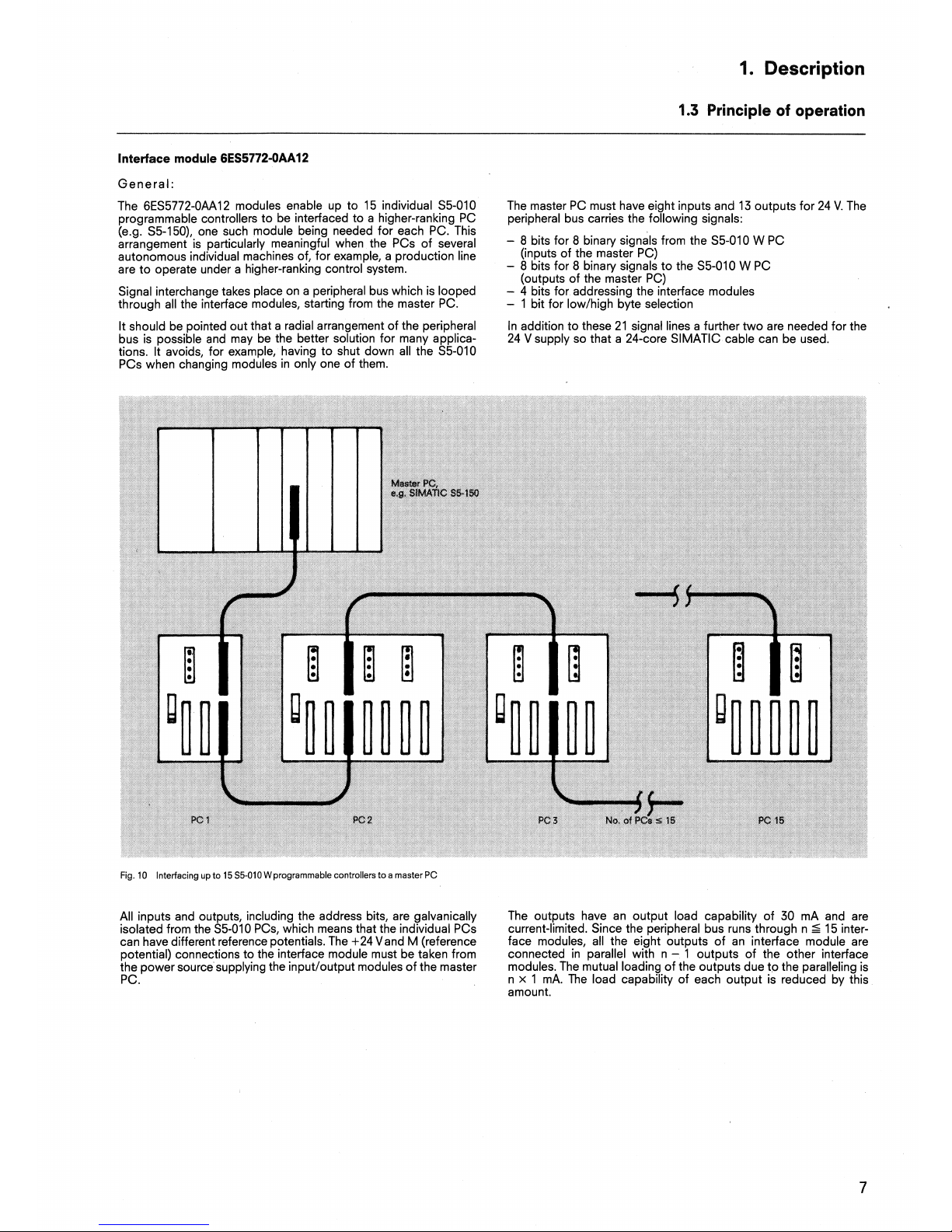
Interface
module
6ES5772-OAA12
General:
The
6ES5772-OAA12 modules enable up to 15 individual S5-010
The master PC
must have eiaht inputs and
13
outputs for 24 V. The
programmable controllers to be interfaced to a higher-ranking PC peripheral bus carries the
fdlowing signals:
(e.g.
S5-150), one such module being needed for each PC. This
arrangement is particularly meaningful when the
PCs of several
-
8
bits for 8 binary signals from the SS-010 W PC
autonomous individual machines of, for example, a production line
(inputs of the master PC)
are to oaerate under a hiaher-rankina control svstem.
-
8
bits for 8 binary signals to the S5-010 W PC
v
(outputs of the master PC)
Signal interchange takes place on a peripheral bus which is looped
-
4 bits for addressing the interface modules
through all the interface modules, starting from the master PC.
-
1 bit for lowlhigh byte selection
It should be pointed out that a radial arrangement of the peripheral
In addition to these 21 signal lines a further two are needed for the
bus is possible and may be the better solution for many applica-
24 V supply so that a 24-core
SlMATlC cable can be used.
tions. It avoids, for example, having to shut down all the S5-010
PCs when changing modules in only one of them.
Fig.
10 Interfacing
up
to 15 55-010 Wprogrammable controllers to a master
PC
PC
2
PC;
3
No
of
Es
5
15
All inputs and outputs, including the address bits, are galvanically The outputs have an output load capability of 30 mA and are
isolated
from the S5-010 PCs, which means that the individual PCs
current-limited. Since the peripheral bus runs through n d 15 inter-
can have different reference potentials. The +24 Vand
M
(reference face modules, all the eight outputs of an interface module are
potential) connections to the interface module must be taken from
connected in parallel with n
-
1
outputs of the other interface
the power source supplying the
inputloutput modules of the master
modules. The mutual loading of the outputs due to the paralleling is
PC.
n
X
1 mA. The load capability of each output is reduced by this
amount.
 Loading...