


ICs for Consumer Electronics
Quarter PIP Processor
SDA 9189X (A123 / A132)
4PIP
Data Sheet 03.96

Edition 03.96
This edition was realized using the software
system FrameMaker
.
Published by Siemens AG,
Bereich Halbleiter, MarketingKommunikation, Balanstraße 73,
81541 München
Siemens AG 1996.
All Rights Reserved.
Attention please!
As far as patents or other rights of third parties are concerned, liability is only assumed
for components, not for applications, processes and circuits implemented within components or assemblies.
The information describes the type of component and shall not be considered as assured
characteristics.
Terms of delivery and rights to change design
reserved.
For questions on technology, delivery and
prices please contact the Semiconductor
Group Offices in Germany or the Siemens
Companies and Representatives worldwide
(see address list).
Due to technical requirements components
may contain dangerous substances. For information on the types in question please
contact your nearest Siemens Office, Semiconductor Group.
Siemens AG is an approved CECC manufacturer.
Packing
Please use the recycling operators known to
you. We can also help you – get in touch with
your nearest sales office. By agreement we
will take packing material back, if it is sorted.
You must bear the costs of transport.
For packing material that is returned to us unsorted or which we are not obliged to accept,
we shall have to invoice you for any costs incurred.
Components used in life-support devices
or systems must be expressly authorized
for such purpose!
Critical components
Group of Siemens AG, may only be used in
life-support devices or systems
1
of the Semiconductor
2
with the express written approval of the Semiconductor
Group of Siemens AG.
1 A critical component is a component used
in a life-support device or system whose
failure can reasonably be expected to
cause the failure of that life-support device or system, or to affect its safety or effectiveness of that device or system.
2 Life support devices or systems are in-
tended (a) to be implanted in the human
body, or (b) to support and/or maintain
and sustain human life. If they fail, it is
reasonable to assume that the health of
the user may be endangered.
SDA 9189X
Revision History: Current Version: 03.96
Previous Version:
Page
(in previous
Version)
Page
(in new
Version)
15 26.01.1994: not allowed display areas, display position
30 26.01.1994: character ‘m’ instead of ‘%’
32 26.01.1994: bit D6 of register 0F inverted
36 26.01.1994: adjustment values VSIDEL
38 26.01.1994: DA converter
30 08.04.1994: character ‘&’ instead of ‘!’
35; 38 08.04.1994: text subaddress 06 and 0F
38 08.04.1994: output voltage ANACON
41 08.04.1994: supply voltage range
24 20.09.1994: examples for the adjustment of frame colors
32; 36 20.09.1994: new I2C bits VSIISQ and VSPISQ
33 20.09.1994: notes at subaddress 00; bits D1 and D3
Subjects (major changes since last revision)
26.01.1994: Target Specification
34 20.09.1994: note & warning at subaddress 02
35 20.09.1994: warning at subaddress 06
36 20.09.1994: warning at subaddress 07
38 20.09.1994: elimination of bit d6 of subaddress 0F
41 20.09.1994: output voltage
43 20.09.1994: remark for series resistance
46 20.09.1994: values supply current
47 20.09.1994: values DAC current
49 20.09.1994: new diagram
51; 52 20.09.1994: new application circuit and layout proposal

SDA 9189X
Table of Contents Page
1 General Description . . . . . . . . . . . . . . . . . . . . . . . . . . . . . . . . . . . . . . . . . . . 6
1.1 Features . . . . . . . . . . . . . . . . . . . . . . . . . . . . . . . . . . . . . . . . . . . . . . . . . . . . . 7
1.2 Pin Configuration . . . . . . . . . . . . . . . . . . . . . . . . . . . . . . . . . . . . . . . . . . . . . . 9
1.3 Pin Definitions and Functions . . . . . . . . . . . . . . . . . . . . . . . . . . . . . . . . . . . . 10
1.4 Functional Block Diagram . . . . . . . . . . . . . . . . . . . . . . . . . . . . . . . . . . . . . . 12
2 System Description . . . . . . . . . . . . . . . . . . . . . . . . . . . . . . . . . . . . . . . . . . 13
2.1 Display Modes . . . . . . . . . . . . . . . . . . . . . . . . . . . . . . . . . . . . . . . . . . . . . . . 13
2.2 Input Signal Processing . . . . . . . . . . . . . . . . . . . . . . . . . . . . . . . . . . . . . . . . 19
2.2.1 Data Transfer . . . . . . . . . . . . . . . . . . . . . . . . . . . . . . . . . . . . . . . . . . . . . . . . 19
2.2.2 Decimation Window . . . . . . . . . . . . . . . . . . . . . . . . . . . . . . . . . . . . . . . . . . . 19
2.2.3 Decimation Filters . . . . . . . . . . . . . . . . . . . . . . . . . . . . . . . . . . . . . . . . . . . . 20
2.3 PIP Field Memory . . . . . . . . . . . . . . . . . . . . . . . . . . . . . . . . . . . . . . . . . . . . . 21
2.3.1 Picture Sizes . . . . . . . . . . . . . . . . . . . . . . . . . . . . . . . . . . . . . . . . . . . . . . . . 21
2.3.2 Memory Writing . . . . . . . . . . . . . . . . . . . . . . . . . . . . . . . . . . . . . . . . . . . . . . 21
2.3.3 Memory Reading and Synchronization to Parent Channel . . . . . . . . . . . . . 22
2.4 Output Signal Processing . . . . . . . . . . . . . . . . . . . . . . . . . . . . . . . . . . . . . . . 22
2.4.1 Display Position . . . . . . . . . . . . . . . . . . . . . . . . . . . . . . . . . . . . . . . . . . . . . . 22
2.4.2 Line Standard of the PIP Picture . . . . . . . . . . . . . . . . . . . . . . . . . . . . . . . . . 23
2.4.3 Interpolation of the Chrominance Signals . . . . . . . . . . . . . . . . . . . . . . . . . . 23
2.4.4 Framing . . . . . . . . . . . . . . . . . . . . . . . . . . . . . . . . . . . . . . . . . . . . . . . . . . . . 24
2.4.5 Full Screen Background Insertion . . . . . . . . . . . . . . . . . . . . . . . . . . . . . . . . 24
2.4.6 Filling PIP Picture with Color . . . . . . . . . . . . . . . . . . . . . . . . . . . . . . . . . . . . 25
2.4.7 Wipe-In/Wipe-Out Facility . . . . . . . . . . . . . . . . . . . . . . . . . . . . . . . . . . . . . . 25
2.4.8 Output Formats and RGB Conversion . . . . . . . . . . . . . . . . . . . . . . . . . . . . . 25
2.4.9 Matrix Equations . . . . . . . . . . . . . . . . . . . . . . . . . . . . . . . . . . . . . . . . . . . . . 26
2.4.10 Select Signal . . . . . . . . . . . . . . . . . . . . . . . . . . . . . . . . . . . . . . . . . . . . . . . . 26
2.4.11 Blanking Signals . . . . . . . . . . . . . . . . . . . . . . . . . . . . . . . . . . . . . . . . . . . . . . 26
2.4.12 Pedestal for the Chrominance Signals . . . . . . . . . . . . . . . . . . . . . . . . . . . . . 26
2.5 Digital-to-Analog Conversion . . . . . . . . . . . . . . . . . . . . . . . . . . . . . . . . . . . . 27
2.5.1 Analog Video Outputs . . . . . . . . . . . . . . . . . . . . . . . . . . . . . . . . . . . . . . . . . 27
2.5.2 Analog Control Signal . . . . . . . . . . . . . . . . . . . . . . . . . . . . . . . . . . . . . . . . . 27
2.6 On-Screen Display . . . . . . . . . . . . . . . . . . . . . . . . . . . . . . . . . . . . . . . . . . . . 27
2.6.1 Display Format . . . . . . . . . . . . . . . . . . . . . . . . . . . . . . . . . . . . . . . . . . . . . . . 27
2.6.2 Character Programming . . . . . . . . . . . . . . . . . . . . . . . . . . . . . . . . . . . . . . . . 27
2.6.3 Character and Character Background Luminance . . . . . . . . . . . . . . . . . . . . 28
2.6.4 Character Set . . . . . . . . . . . . . . . . . . . . . . . . . . . . . . . . . . . . . . . . . . . . . . . . 29
2.7 Numerical PLL . . . . . . . . . . . . . . . . . . . . . . . . . . . . . . . . . . . . . . . . . . . . . . . 30
2.8 I
2.8.1 I
2.8.2 I
2.8.3 I
2
C Bus . . . . . . . . . . . . . . . . . . . . . . . . . . . . . . . . . . . . . . . . . . . . . . . . . . . . . 30
2
C Bus Addresses . . . . . . . . . . . . . . . . . . . . . . . . . . . . . . . . . . . . . . . . . . . . 30
2
C Bus Receiver Format . . . . . . . . . . . . . . . . . . . . . . . . . . . . . . . . . . . . . . . 30
2
C Bus Commands . . . . . . . . . . . . . . . . . . . . . . . . . . . . . . . . . . . . . . . . . . . 31
Semiconductor Group 4 03.96

SDA 9189X
Table of Contents Page
3 Electrical Characteristics . . . . . . . . . . . . . . . . . . . . . . . . . . . . . . . . . . . . . 40
3.1 Absolute Maximum Ratings . . . . . . . . . . . . . . . . . . . . . . . . . . . . . . . . . . . . . 40
3.2 Operational Range . . . . . . . . . . . . . . . . . . . . . . . . . . . . . . . . . . . . . . . . . . . . 41
3.3 Characteristics . . . . . . . . . . . . . . . . . . . . . . . . . . . . . . . . . . . . . . . . . . . . . . . 45
4 Diagrams . . . . . . . . . . . . . . . . . . . . . . . . . . . . . . . . . . . . . . . . . . . . . . . . . . . 48
4.1 Output Current of DA Converters . . . . . . . . . . . . . . . . . . . . . . . . . . . . . . . . . 48
4.2 Application Information . . . . . . . . . . . . . . . . . . . . . . . . . . . . . . . . . . . . . . . . . 50
4.2.1 Application Circuit . . . . . . . . . . . . . . . . . . . . . . . . . . . . . . . . . . . . . . . . . . . . 50
4.2.2 Application Board Layout Proposal . . . . . . . . . . . . . . . . . . . . . . . . . . . . . . . 51
4.3 Waveforms . . . . . . . . . . . . . . . . . . . . . . . . . . . . . . . . . . . . . . . . . . . . . . . . . . 52
4.3.1 Phase Relation of Sync Pulses at Frame Mode . . . . . . . . . . . . . . . . . . . . . . 52
5 Package Outlines . . . . . . . . . . . . . . . . . . . . . . . . . . . . . . . . . . . . . . . . . . . . 54
I2C Bus
2
Purchase of Siemens I
to use the components in the I
C components conveys the license under the Philips I2C patent
2
C system provided the system conforms to the I2C
specifications defined by Philips.
Semiconductor Group 5 03.96

SDA 9189X
1 General Description
The Picture Insertion Processor SDA 9189X generates a reduced size picture of an inset
video channel for the purpose of combining it with another video signal (parent channel).
The easy implementation of the IC into an existing system needs only a few additional
external components. There is a great variety of application facilities in consumer and
professional products (TV sets, VCRs, supervising monitors, multi-media, etc.).
Semiconductor Group 6 03.96
Quarter PIP Processor SDA 9189X
Data Sheet
1.1 Features
• High system integration
Filtering, field memory, RGB-matrix,
DA-Conversion, clock generation, and control
circuits integrated on one chip
• 4 picture sizes
1/4th, 1/9th, 1/16th, or 1/36th of normal size
• High resolution display
13.5 MHz/27 MHz display clock frequency
288 luminance and 72 chrominance pixels per inset line for picture size 1/4
6-bit amplitude resolution for each incoming signal component
Frame mode display in single-PIP modes
Horizontal and vertical filtering
Special antialias filtering for the luminance signal
P-DSO-32-2
• Single and multi PIP display
Up to 9 pictures of 1/36th size (8 still and 1 moving)
Up to 4 pictures of 1/16th size (3 still and 1 moving)
Up to 2 pictures of 1/9th size (1 still and 1 moving)
Up to 3 pictures of 1/9th size (2 still and 1 moving) as POP display in 16:9 TV sets
(In multi-PIP modes only field mode display possible)
• Multistandard applications
Automatic recognition of 625 lines/525 lines standard (inset and parent channel)
Scan conversion systems as flickerfree display systems (parent channel)
• HDTV (parent channel)
• 16:9 compatibility
Operation in 4:3 and 16:9 TV sets
4:3 inset signals on 16:9 displays (picture size 1/4 and 1/9)
16:9 inset signals on 4:3 displays (picture size 1/9 and 1/16)
Type Ordering Code Package
SDA 9189X Q67100-H5148 P-DSO-32-2
Semiconductor Group 7 03.96

SDA 9189X
• Digital inputs
Y, + (B-Y), + (R-Y)
Compatible with Triple ADC SDA 9187-2X
• Analog outputs
Y, + (B-Y), + (B-Y) or Y, – (B-Y), – (B-Y) or RGB
3 RGB-matrices: EBU, NTSC (Japan), NTSC (USA)
• Digital to analog converter output e.g. for color decoder adjustment
6-bit resolution
• Freely programmable position of inset picture
Steps of 1 pixel and 1 line
All PIP and POP positions are possible inside the standard display area
• Programmable framing
4096 frame colors
Variable frame width
• Full screen background insertion
64 background colors or transparent display (parent picture seen)
• Wipe-in/Wipe-out facility
Start and end of insertion is the lower right PIP corner
4 periods programmable
• Freeze picture
• I2C Bus control
• Up to three ICs in one application
2
Three different I
C Bus addresses
Up to 3 moving pictures using 3 ICs
Up to 27 pictures of 1/36th size
• On-screen display of channel index
64 characters programmable (alphanumeric and special symbols)
5 characters displayed in every PIP picture
4 different character luminance values (B-Y = R-Y = ‘0’)
4 background luminance values (B-Y = R-Y = ‘0’) or transparent mode
(inset picture seen)
• Numerical display PLL circuit for high stability clock generation
• No necessity of PAL/SECAM delay lines when using suitable color decoders
• P-DSO-32 package/350 mil (SMD)
• 5 V supply voltage
Semiconductor Group 8 03.96
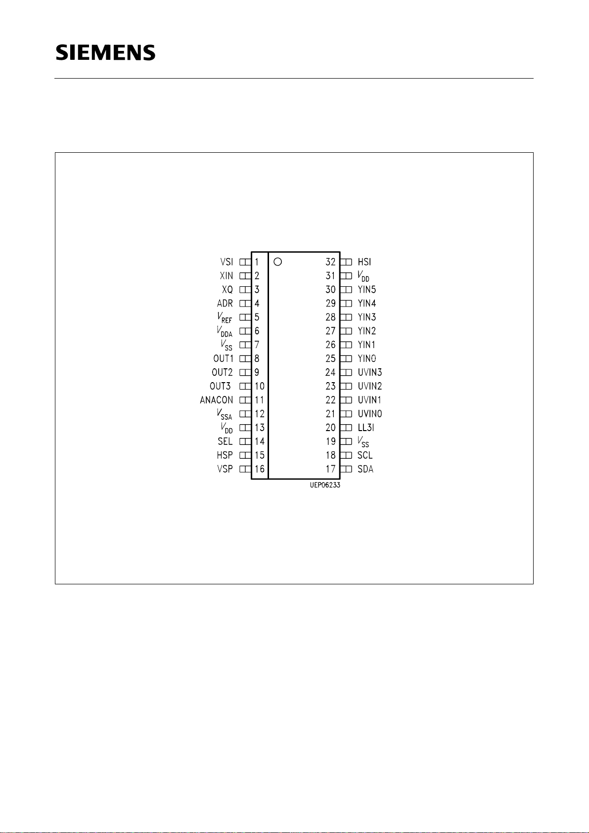
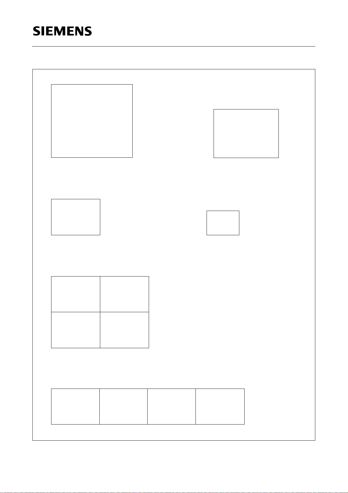
1.2 Pin Configuration
(top view)
SDA 9189X
P-DSO-32-2
Figure 1
Semiconductor Group 9 03.96
1.3 Pin Definitions and Functions
1)
Pin No. Symbol Function
Descriptions
1 VSI I/TTL Inset vertical sync input
2 XIN I PLL quartz oscillator input
3 XQ Q PLL quartz oscillator output
SDA 9189X
4 ADR I
5
6
7
V
V
V
REF
DDA
SS
3-L
I/ana DACs reference voltage
S DACs and PLL positive voltage supply
S Digital ground
I2C address
8 OUT1 Q/ana Analog output R or + (R-Y) or – (R-Y)
9 OUT2 Q/ana Analog output G or Y
10 OUT3 Q/ana Analog output B or + (B-Y) or – (B-Y)
11 ANACON Q/ana Analog output (e.g. color decoder adjustment)
12
13
V
V
SSA
DD
S DACs and PLL ground
S Digital positive voltage supply
14 SEL Q/var Signals OUT1 - OUT3 valid
15 HSP I/TTL Parent horizontal sync input
16 VSP I/TTL Parent vertical sync input
17 SDA IQ/TTL I
18 SCL I/TTL I
2
C data input/output
2
C clock
19
V
SS
S Digital ground
20 LL3I I/TTL Line locked clock inset picture
21 UVIN0 I/TTL Digital UV input data
22 UVIN1 I/TTL Digital UV input data
23 UVIN2 I/TTL Digital UV input data
24 UVIN3 I/TTL Digital UV input data
1)
S: supply, I: input, Q: output, TTL: digital (TTL), ana: analog, 3-L: 3 level signal,
var: variable configuration of output stage (open source, open drain, TTL)
Semiconductor Group 10 03.96
1.3 Pin Definitions and Functions (cont’d)
1)
Pin No. Symbol Function
Descriptions
25 YIN0 I/TTL Digital Y input data
26 YIN1 I/TTL Digital Y input data
27 YIN2 I/TTL Digital Y input data
28 YIN3 I/TTL Digital Y input data
29 YIN4 I/TTL Digital Y input data
30 YIN5 I/TTL Digital Y input data
SDA 9189X
31
V
DD
S Digital positive voltage supply
32 HSI I/TTL Inset horizontal sync input
1)
S: supply, I: input, Q: output, TTL: digital (TTL), ana: analog, 3-L: 3 level signal,
var: variable configuration of output stage (open source, open drain, TTL)
Semiconductor Group 11 03.96
1.4 Functional Block Diagram
SDA 9189X
Figure 2
Semiconductor Group 12 03.96
SDA 9189X
2 System Description
2.1 Display Modes
8 single- and 10 multi-PIP display modes are available. Decimation, memory controlling,
framing and on-screen display insertion depend on the selected display mode
(PIPMOD).
In the multi-PIP modes the complete inset picture can contain up to 9 partial pictures
(see diagrams below). One of the partial pictures shows a moving picture, whereas the
others show still pictures. The partial picture that has to be written is addressed via
2
C Bus. The addresses (WRPOS) for the individual pictures are shown in the diagrams.
I
The same addresses serve to choose the position of the moving picture. The multi-PIP
modes allow tuner scanning.
Four display modes are provided for applications with 16:9 inset signals or displays
(see table 1). The single-PIP display modes 15 and 18 can be used to display 4:3 inset
signals on 16:9 displays. To show 16:9 inset signals on 4:3 displays the single-PIP
display modes 16 and 19 have been added. By means of multi-PIP display mode 17
a POP picture on a 16:9 display can be created.
If a display mode is chosen that is not realized (modes 9, 12, and 20 to 31), the
PIP insertion is switched off automatically (PIPON = ‘0’).
Table 1
Display Mode (PIPMOD) Picture Size, Picture Configuration
0 (00000) 1 × 1/4
1 (00001) 1 × 1/9
2 (00010) 1 × 1/16
3 (00011) 1 × 1/36
4 (00100) 4 × 1/16, 2 rows of 2 pictures
5 (00101) 4 × 1/16, side by side
6 (00110) 4 × 1/16, one upon another
7 (00111) 9 × 1/36, 3 rows of 3 pictures
8 (01000) 2 × 1/9, side by side
9 (01001) Not realized (PIPON = ‘0’)
10 (01010) 8 × 1/36, 2 rows of 4 pictures
11 (01011) 2 × 1/9, one upon another
12 (01100) Not realized (PIPON = ‘0’)
13 (01101) 8 × 1/36, 2 columns of 4 pictures one upon another
Semiconductor Group 13 03.96
SDA 9189X
Table 1(cont’d)
Display Mode (PIPMOD) Picture Size, Picture Configuration
14 (01110) 4 × 1/36, 2 rows of 2 pictures
15 (01111) 1 × 1/9, 4:3 inset signal on 16:9 display horizontal
decimation 4:1, vertical decimation 3:1
16 (10000) 1 × 1/16, 16:9 inset signal on 4:3 display horizontal
decimation 3:1, vertical decimation 4:1
17 (10001) 3 × 1/9, 4:3 inset signals on 16:9 display horizontal
decimation 4:1, vertical decimation 3:1 one
upon another
18 (10010) 1 × 1/4, 4:3 inset signal on 16:9 display horizontal
decimation 3:1, vertical decimation 2:1
19 (10011) 1 × 1/9, 16:9 inset signal on 4:3 display horizontal
decimation 2:1, vertical decimation 3:1
20 (10100)
:
Not realized (PIPON = ‘0’)
31 (11111)
The following diagrams show the various display modes. The figures on top of the
rectangles give the width of the complete inset picture in pixels whereas the figures on
the right specify its height by the number of lines. The values for the multi-PIP display
modes are obtained by adding the widths and heights of the partial pictures. The sizes
of the partial pictures correspond to the sizes of the inset pictures of the single-PIP
modes (see below).
Semiconductor Group 14 03.96
288
SDA 9189X
192
Mode 0
144
Mode 2
0
126
(102)
0
84
(68)
Mode 1
96
0
63
(51)
0
42
(34)
Mode 3
288
Mode 4
Mode 5
Figure 3
01
126
(102)
23
576
0123
63
(51)
Semiconductor Group 15 03.96
SDA 9189X
144
0
1
2
3
Mode 6
252
(204)
Mode 8
288
012
345
126
(102)
678
Mode 7
384
01
64
(68)
384
0123
4567
Mode 10
192
01
23
168
(136)
45
The display modes 9 and 12 are not realized.
For a PIP display line standard of 525 lines
67
the values in parenthesis are valid.
84
(68)
192
0
168
(136)
1
Mode 11
Mode 13
Figure 4
Semiconductor Group 16 03.96
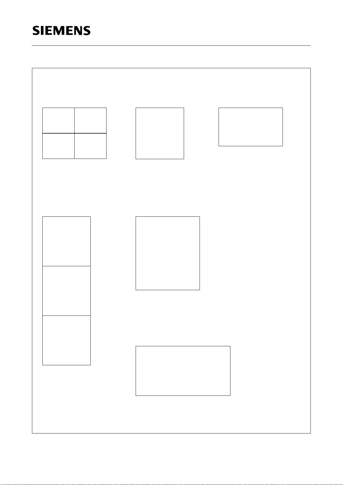
SDA 9189X
192
01
23
Mode 14
144
0
84
(68)
144
0
Mode 15
192
0
84
(68)
126
(102)
Mode 16
192
0
63
(51)
Mode 17
Figure 5
1
2
252
(204)
Mode 18
Mode 19
288
0
84
(68)
Semiconductor Group 17 03.96

SDA 9189X
2 ARD
1
-
3 ZDF
-
4 RTL
-
Figure 6
Multi-POP Feature at 16:9 Application with Display Mode 7 and OSD
Main picture and one POP picture live, all other pictures still
5 SFB
-
7 HR
-
2 ARD
-
6 ORF
-
8 NTV
-
3 ZDF
-
1 NDR
-
4 RTL
-
9 DFS
-
Figure 7
Multi-PIP Feature with Display Mode 7
Main picture and one PIP picture live, all other pictures still
Semiconductor Group 18 03.96

SDA 9189X
2.2 Input Signal Processing
2.2.1 Data Transfer
The inset video signal is accepted as digital luminance and chrominance components
with a 13.5 MHz clock for the luminance signal and a 3.375 MHz clock for the
chrominance signals.
Inset synchronization is done via pin HSI for horizontal and pin VSI for vertical
synchronization. By analyzing the synchronization pulses the line standard of the inset
signal source is detected and interference noise on the vertical sync signal is removed.
For applications with fixed line standard (625 lines or 525 lines) the automatic detection
can be switched OFF.
The phase of the vertical sync pulse is programmable (VSIDEL) (see chapter 4.3). This
way a correct detection of the field number is possible, an important condition for frame
mode display.
2.2.2 Decimation Window
A window signal, derived from the sync pulses and the detected line standard, defines
the part of the active video area used for decimation. The window has a width of
576 pixels for the luminance signal and a width of 144 pixels for the chrominance
signals. In the vertical direction the window consists of 252 or 204 lines depending on
the line standard (625 or 525 lines respectively).
The horizontal position of this decimation window can be adapted to various applications
with the help of a programmable delay of the luminance signal (HSIDEL) relative to the
horizontal synchronization pulses. For HSIDEL = ‘0’ the decimation window is opened
0 clock periods (13.5 MHz) after the horizontal synchronization pulse. For the 625 lines
standard the 42th video line is the first decimated line, for the 525 lines standard
decimation starts in the 38th video line.
Semiconductor Group 19 03.96

SDA 9189X
2.2.3 Decimation Filters
The input signal is decimated by subsampling with horizontal and vertical filtering. A
special antialias filter improves the frequency response of the luminance channel.
The following decimation filters are implemented:
Horizontal Decimation Luminance Filter Chrominance Filter
2:1 { 1 1 } { 1 1 }
3:1 { 1 1 1 } { 1 2 1 }
4:1 { 1 1 1 1 } { 1 1 1 1 }
6:1 { 1 1 1 1 1 1 } { 1 1 2 2 1 1 }
Vertical Decimation Luminance Filter Chrominance Filter
2:1 { 1 1 } { 1 1 }
3:1 { 1 1 1 } { 1 2 1 }
4:1 { 1 1 1 1 } { 1 1 1 1 }
6:1 { 1 1 1 1 1 1 } { 1 1 2 2 1 1 }
The realized chrominance filtering allows omitting the color decoder delay line for PAL
and SECAM demodulation if the color decoder supplies the same output voltages
independent of the kind of operation. In case of SECAM signals an amplification of the
chrominance signals by a factor of 2 is necessary because there is a signal only in every
second line. This chrominance amplification is programmable via I2C Bus (AMSEC).
Semiconductor Group 20 03.96

SDA 9189X
2.3 PIP Field Memory
The on-chip memory has a capacity of 329184 bits. It stores one decimated field of the
inset picture. In the multi-PIP display modes the memory is able to store one decimated
field of every partial picture (e.g. during tuner scanning).
2.3.1 Picture Sizes
The picture size depends on the horizontal and vertical decimation factors.
Horizontal Decimation Pixels/Line
2:1 288
3:1 192
4:1 144
6:1 96
Vertical Decimation Lines/Field
(625 lines standard)
Lines/Field
(525 lines standard)
2:1 126 102
3:1 84 68
4:1 63 51
6:1 42 34
2.3.2 Memory Writing
To get equal clock frequencies for luminance and chrominance signals a multiplexer at
the memory input generates a 3-bit data format for both chrominance components.
In field mode display only every second inset field is written into the memory, in frame
mode display the memory is written continuously. Data are written with the lower inset
clock frequency depending on the horizontal decimation factor (6.75 MHz, 4.5 MHz,
3.375 MHz, or 2.25 MHz).
Memory writing can be stopped by program (FREEZE), a freeze picture display results
(one field).
In single-PIP display modes frame mode display is possible having no scan conversion
and the same number of lines in inset and parent channel (625 lines or 525 lines both).
The result is a higher vertical and temporal resolution because of displaying every
incoming field. The standards are analyzed internally and an activated frame mode
display is switched to field mode display automatically when the described restrictions
are no longer valid.
Semiconductor Group 21 03.96

SDA 9189X
2.3.3 Memory Reading and Synchronization to Parent Channel
The reading frequency is normally 13.5 MHz and 27 MHz for scan conversion systems.
For progressive scan conversion systems and HDTV displays a line doubling mode is
available (LINEDBL). Every line of the inset picture is read twice.
Synchronization of memory reading with the parent channel is achieved by processing
the parent horizontal and vertical synchronization signals. These signals are fed to the
IC at pin HSP for horizontal synchronization and at pin VSP for vertical synchronization.
A numerical PLL circuit generates a clock signal that is locked to the horizontal
synchronization pulses of the parent channel. The burst gate of the sandcastle signal
can be used for horizontal synchronization.
A field number detection is carried out for the inset channel as well as for the parent
channel. Depending on the phase difference between inset and parent signals a
correction of the display raster for the read out data is performed by omitting or inserting
lines when the read address counter outruns the write address counter.
2.4 Output Signal Processing
2.4.1 Display Position
The display position of the inset picture is freely programmable (POSHOR, POSVER).
The first possible picture position (without frame) is 55 clock periods (13.5 MHz or
27 MHz) after the horizontal and 7 lines after the vertical synchronization pulses.
Starting at this position the picture can be moved over the whole display area. Even POP
positions (Picture Outside Picture) can be used.
Note: Display without disturbances is only possible if the complete PIP picture is inside
the visible area of the picture tube
POSHOR < 1
POSHOR < 864 – 2 × FRWIDH – PSH – 42
POSVER < 262 – 2 × FRWIDV – PSV – 8 (60 Hz mode) or
POSVER < 312 – 2 × FRWIDV – PSV – 8 (50 Hz mode)
POS … = Picture Position (see I
FRWID. = Frame Width (see I
2
C Bus)
2
C Bus)
PSH = Picture size horizontal (number of pixels)
PSV = Picture size vertical (number of line)
Semiconductor Group 22 03.96

SDA 9189X
2.4.2 Line Standard of the PIP Picture
2
The line standard used to display the complete PIP picture is programmable via I
(PIPLIN). The line standard of the parent channel or the inset channel can be used. In
addition a fixed line standard of 625 or 525 lines can be chosen.
Combinations of different line standards of the inset signal and the PIP display are
handled in a special way:
PIP display 625 lines, inset signal 525 lines
– The inset picture is shifted down by 12, 8, 6, or 4 lines according to picture size. Due
to this shift the centres of the inset pictures have the same position for both line
standards. The remaining 12, 8, 6, or 4 lines at the top and the bottom of the inset
picture are filled with the luminance value of the full screen background color (BCKY).
The chrominance values are set to ‘0’ for these parts of the inset picture.
C Bus
PIP display 525 lines, inset signal 625 lines
– The inset picture is reduced to 102, 68, 51, or 34 lines. Depending on the number of
lines the first and the last 12, 8, 6, or 4 lines are omitted. In this way the display shows
the centre part of the original picture.
Displaying multi-PIP pictures this procedure is applied individually to each of the partial
pictures.
2.4.3 Interpolation of the Chrominance Signals
At the memory output the chrominance components are demultiplexed and linearly
interpolated to the luminance sampling rate.
Semiconductor Group 23 03.96

SDA 9189X
2.4.4 Framing
In this part of the circuit a colored frame is added to the inset picture. 4096 frame colors
are programmable, 4 bits for each component Y, (B-Y), (R-Y). The horizontal and vertical
widths of the frame are independently programmable. In the multi-PIP modes the various
partial pictures are separated by inner frame elements. These parts of the frame have a
fixed horizontal width of 4 pixels and a fixed vertical width of 2 lines. For INFR = ‘0’ the
inner frame elements are not inserted.
The outer frame elements border on the inset picture without limiting its size whereas the
inner frame elements reduce the areas of the partial pictures.
Examples for the Adjustment of Frame Colors
Frame Color FRY
D3 … D0 of
Subaddress 09
FRU
D3 … D0 of
Subaddress 0A
FRV
D7 … D4 of
Subaddress 0A
Blue 0100 0110 1010
Green 0100 1000 1010
White 1100 0000 0000
Red 0100 1000 0111
Yellow 1100 1000 0100
Cyan 1100 0010 1010
Magenta 0100 0110 0100
2.4.5 Full Screen Background Insertion
Instead of showing the parent picture it is possible to fill the background (full screen
picture without inset picture and its frame, BCKON = ‘1’) with a programmable color.
For BCKFR = ‘1’ the background color is identical with the frame color, otherwise it is
defined by 6 bits programmable via I
2
C Bus: two bits for each component. The bits for
the chrominance signals are used directly as MSBs of the output words B-Y and R-Y.
The remaining LSBs are set to ‘0’. Therefore 16 different colors are possible. The two
bits for the Y-signal choose a luminance value according to the following table (100 IRE
corresponds to the full scale range of DAC input = integer value 63):
Background Luminance IRE Integer Value
0 0 20 12
0 1 30 19
1 0 40 25
1 1 50 31
Semiconductor Group 24 03.96

SDA 9189X
2.4.6 Filling PIP Picture with Color
The whole inset picture can be filled with the frame color (FRCOL = ‘1’) or the luminance
value for the full screen background insertion without colors (BCKCOL = ‘1’,
FRCOL = ‘0’). The frame elements remain visible. Filling the PIP picture with
background is especially useful before starting a tuner scanning cycle.
2.4.7 Wipe-In/Wipe-Out Facility
With the wipe-in/wipe-out function it is possible to make appear or disappear the
complete inset picture starting or ending at the lower right corner of the inset picture
position. Thereby the size of the picture is continuously increased and decreased
respectively. During this procedure the frame is shown with its chosen widths. 4 different
periods are programmable via I
2.4.8 Output Formats and RGB Conversion
2
C Bus.
Different output formats are available: luminance signal Y with inverted or non-inverted
chrominance signals (B-Y), (R-Y) or RGB signals.
For the RGB conversion 3 matrices are provided:
Standard Amplitudes Angles
B-Y R-Y G-Y B-Y R-Y G-Y
EBU 1 0.558 0.345 0° 90° 237°
NTSC (Japan) 1 0.783 0.31 0° 95° 240°
NTSC (USA) 1 1.013 0.305 0° 104° 252°
2
Matrix selection is done via I
C Bus. The matrices are designed for the following
voltages at the inputs of the ADC converter (the values correspond to 100 % white and
75 % color saturation):
Component Input Voltage (without Sync)
in % of Full Scale Input Range of ADC
Y75
B-Y 100
R-Y 100
Semiconductor Group 25 03.96

2.4.9 Matrix Equations
SDA 9189X
EBU
R
G
B
R
G
B
=
=
101
0.25– 0.78125 1
0.1875– 0.40625– 1
NTSC (Japan)
101
0.0625– 1.09375 1
0.15625– 0.375– 1
BY–
RY–
Y
BY–
RY–
Y
NTSC (USA)
R
G
B
=
101
0.25– 1.375 1
BY–
RY–
0.09375– 0.40625– 1
Y
2.4.10 Select Signal
For controlling an external fast switch (for example an RGB processor) a select signal
SEL is supplied. The delay of this signal relative to the luminance and chrominance
components is programmable for adaption to different external output signal
Semiconductor Group 26 03.96

SDA 9189X
processings. Three different characteristics of the output stage of this signal are
available. An open source, an open drain, or a TTL output can be selected via I
(SELMOD).
2.4.11 Blanking Signals
In case of full screen background insertion the circuit has to generate output signals with
correctly positioned line blanking intervals relative to the horizontal synchronization
pulses of the parent channel. This can be achieved by a programmable delay (BLKDEL).
A field-blanking interval with a length of 16 lines is also provided. It is triggered by the
vertical synchronization pulse of the parent channel (VSP). The generation of this
field-blanking signal can be activated via I
2
C Bus (VERBLK = ‘1’).
2.4.12 Pedestal for the Chrominance Signals
Both components of the chrominance signal are equipped with a programmable
pedestal (white balance, PEDESTU, PEDESTV). The pedestal values are fed to the
digital to analog converters during the line blanking intervals. For each component a 4-bit
2
value in 2’s complement code is defined via I
C Bus. Building up the 6-bit input words of
the digital to analog converters these 4 bits are used as LSBs. The missing two MSBs
are complemented by sign extension. In this way pedestal values from – 8 to + 7 LSBs
of the digital to analog converters can be achieved.
2
C Bus
2.5 Digital-to-Analog Conversion
2.5.1 Analog Video Outputs
The IC includes three 6-bit digital to analog converters for the video outputs. Each
V
converter supplies a current through an external resistor that is placed between
SSA
and
OUT1, OUT2, OUT3 respectively. The current is controlled by a digital control circuit.
2.5.2 Analog Control Signal
The additional 6-bit digital to analog converter that provides an analog control signal
(e.g. for color decoder adjustment) is fed directly by a 6-bit signal programmable via
2
C Bus. No external resistor is needed at output ANACON.
I
2.6 On-Screen Display
2.6.1 Display Format
The on-screen display allows to insert a block of 5 characters into each of the PIP
pictures. The characters are placed in a box (background) with a width of 64 pixels and
a height of 12 lines. This box is situated in the upper left corner of the PIP pictures. The
Semiconductor Group 27 03.96

SDA 9189X
background box can be made transparent (CHARBCK = ‘0’), i.e. behind the characters
the inset picture becomes visible.
64 different characters are stored in a character ROM (see table 2). Each character is
defined by a pixel matrix consisting of 10 lines and 12 pixels per line.
2.6.2 Character Programming
2
The 5 characters per block are programmable via I
identical with the ASCII code except for some of the special characters. The codes are
placed in a character RAM consisting of 45 cells. The size of the RAM is determined by
the number of characters per block (5) and the maximum number of PIP pictures (9 in
multi-PIP display modes). The character codes can be transmitted in two ways: each of
the 45 RAM locations can be reached separately by its 7-bit address or the RAM can be
written consecutively starting at an arbitrarily chosen position. In this case the RAM
address is increased automatically.
C Bus using a 7-bit code which is
The 7-bit address consists of two parts: the 4 MSBs are used to choose one of the partial
pictures and the 3 LSBs to select one of the 5 characters per block.
Semiconductor Group 28 03.96

SDA 9189X
2.6.3 Character and Character Background Luminance
The chrominance components of the characters and their background box always have
2
the value ‘0’. The luminance values are programmable via I
following tables (100 IRE corresponds to the full scale range of DAC input = integer
value 63):
Table 2
IRE Integer Value
Character Luminance
0 0 60 38
0 1 70 44
1 0 80 50
C Bus according to the
1 1 90 56
Character Background Luminance
0 0 10 6
0 1 20 12
1 0 30 19
1 1 40 25
Semiconductor Group 29 03.96

2.6.4 Character Set
SDA 9189X
0000001=01 0000010=02 0000011=03
0001001=09
0101010=2A 0101011=2B 0101101=2D 0110000=30 0110001=31 0110010=32 0110011=33
0110100=34
0111110=3E 1000001=41 1000010=42 1000011=43 1000100=44
0001010=0A
0110101=35
0001011=0B
0110110=36 0111000=38 0111001=39
0000100=04
0100000=20
0101111=2F
0000101=05 0000110=06 0001000=08
0100001=21
0100011=23
0000111=07
0100100=24
0111100=3C
1000101=45
0100101=25
0111101=3D0110111=37
1000110=460111111=3F
1000111=47 1001001=49 1001010=4A
1001111=4F
1010111=57 1011001=59
1011000=58 1011011=5B
1010001=51 1010010=52 1010100=54
1011010=5A 1011110=5E 1011111=5F
1001011=4B
1010011=53
1001100=4C 1001101=4D 1001110=4E1001000=48
1011101=5D
1010101=55
1010110=561010000=50
Figure 8
This figure shows the pixel matrices of the characters stored in the character ROM.
Semiconductor Group 30 03.96

SDA 9189X
2.7 Numerical PLL
A numerical PLL circuit supplies a clock of about 27 MHz with high stability. The nominal
quartz frequency is 20.48 MHz. The generated clock is locked to the parent horizontal
synchronization pulses. Its frequency varies with the frequency of this signal. Four
different characteristics of the PLL behavior can be chosen to handle synchronization
signals from various sources (PLLTC).
If the PLL is switched OFF an external 13.5 or 27 MHz parent line locked clock can be
fed to the IC. Using up to three SDA 9189X ICs in the same application only one quartz
is necessary.
Note: Before setting bit D3 of subaddress 00 (READ27) noise reduction of the VSP
pulse must be switched OFF (D5 of subaddress 08 = ‘1’).
2.8 I2C Bus
2
2.8.1 I
Three different I
C Bus Addresses
2
C Bus addresses are programmable via pin ADR.
Pin ADR Address (BIN) Address (HEX)
Low level (
SS
or V
) 1 1 0 1 0 1 1 D6
SSA
V
Mid level (open) 1 1 0 1 1 1 0 DC
High level (
2.8.2 I
V
or V
DD
2
C Bus Receiver Format
) 1 1 0 1 1 1 1 DE
DDA
S Address 0 A Subaddress A Data Byte A *** A P
S: Start condition
A: Acknowledge
P: Stop condition
Only write operation is possible. An automatical address increment function is
implemented.
Semiconductor Group 31 03.96

2.8.3 I2C Bus Commands
Overview
SDA 9189X
Sub
add.
(Hex.)
00 0 0 FREEZE PLLOFF READ27 LINEDBL FRAME PIPON
01 0 SELDEL3 SELDEL2 SELDEL1 SELDEL0 VERBLK POSHOR9 POSHOR8
02 POSHOR7 POSHOR6 POSHOR5 POSHOR4 POSHOR3 POSHOR2 POSHOR1 POSHOR0
03 POSVER7 POSVER6 POSVER5 POSVER4 POSVER3 POSVER2 POSVER1 POSVER0
04 0 PIPLIN1 PIPLIN0 PIPMOD4 PIPMOD3 PIPMOD2 PIPMOD1 PIPMOD0
05 WRPOS3 WRPOS2 WRPOS1 WRPOS0 PMOD1 PMOD0 IMOD1 IMOD0
06 0 0 BCKCOL HSIDEL4 HSIDEL3 HSIDEL2 HSIDEL1 HSIDEL0
07 AMSEC 0 VSIISQ VSIDEL4 VSIDEL3 VSIDEL2 VSIDEL1 VSIDEL0
08 0 0 VSPISQ VSPDEL4 VSPDEL3 VSPDEL2 VSPDEL1 VSPDEL0
09 CON3 CON2 CON1 CON0 FRY5 FRY4 FRY3 FRY2
0A FRV5 FRV4 FRV3 FRV2 FRU5 FRU4 FRU3 FRU2
0B INFR SELMOD1 SELMOD0 FRWIDV1 FRWIDV0 FRWIDH2 FRWIDH1 FRWIDH0
0C 0 0 0 0 MAT1 MAT0 CHRPIP OUTFOR
0D 0 PLLTC1 PLLTC0 00000
0E PEDESTV3 PEDESTV2 PEDESTV1 PEDESTV0 PEDESTU3 PEDESTU2 PEDESTU1 PEDESTU0
D7 D6 D5 D4 D3 D2 D1 D0
Data Byte
0F DACONST 0 ANCON5 ANCON4 ANCON3 ANCON2 ANCON1 ANCON0
10 BCKFR BCKY1 BCKY0 BCKU5 BCKU4 BCKV5 BCKV4 BCKON
11 WIPEON WIPESP1 WIPESP0 BLKDEL3 BLKDEL2 BLKDEL1 BLKDEL0 FRCOL
12 0 CHARY1 CHARY0 CHBCKY1 CHBCKY0 CHARBCK CHARRES OSDON
13 0 CHARLOC6 CHARLOC5 CHARLOC4 CHARLOC3 CHARLOC2 CHARLOC1 CHARLOC0
14 0 CHAR6 CHAR5 CHAR4 CHAR3 CHAR2 CHAR1 CHAR0
After switching on the IC the data bytes of all registers are set to ‘0’, the bit PLLOFF is
set to ‘1’
.
Semiconductor Group 32 03.96

SDA 9189X
Detailed Description
Bit Name Function
Subaddress 00
D5 FREEZE 0: moving picture
1: freeze picture
D4 PLLOFF 0: internal PLL ON
1: internal PLL OFF (external clock generation)
D3 READ27 0: PIP display with single-read frequency (13.5 MHz)
1: PIP display with double read frequency (27 MHz)
(see note page 31)
D2 LINEDBL 0: each line of the PIP memory is read once
(normal operation)
1: each line of the PIP memory is read twice
(line doubling for progressive scan conversion systems
in parent channel)
D1 FRAME 0: field mode display
1: frame mode display (if possible).
Correct adjustment of bits VSIDEL, VSPDEL required
(see chapter 4.3).
D0 PIPON 0: PIP insertion OFF
1: PIP insertion ON
Subaddress 01
D6 … D3 SELDEL Delay of output signal at pin SEL (–8…+7 periods of read
frequency clock, programmable in 2’s complement code)
D2 VERBLK 0: clamping level at DAC outputs only during line blanking
intervals
1: clamping level at DAC outputs during line blanking
intervals and field-blanking intervals (16 complete lines
following the vertical synchronization pulse of the parent
channel)
D1 … D0 POSHOR 2 MSBs of POSHOR (see Subaddress 02 on page 34)
Semiconductor Group 33 03.96

SDA 9189X
Detailed Description (cont’d)
Bit Name Function
Subaddress 02
D7 … D0 POSHOR Horizontal position of PIP picture (in steps of 1 pixel)
Note: the 2 MSBs of POSHOR are located at subaddress 01,
bits D0 and D1.
Warning: Positions outside the active area of the parent
picture are possible. Allowed area see at chapter 2.4.1.
To avoid horizontal jumping of the picture by changing
POSHOR from ‘00 1111 1111’ to ‘01 0000 0000’ its
necessary to transfer the bits of both subaddresses during the
same field period.
Subaddress 03
D7 … D0 POSVER Vertical position of PIP picture (in steps of 1 line)
Warning: Positions outside the active area of the parent
picture are possible. Allowed area see at chapter 2.4.1
Subaddress 04
D6 … D5 PIPLIN 00: PIP display line standard according to parent signal
01: PIP display line standard according to inset signal
10: fixed PIP display line standard: 625 lines
11: fixed PIP display line standard: 525 lines
D4 … D0 PIPMOD Display mode (8 single- and 10 multi-PIP display modes are
available, see diagrams above)
Semiconductor Group 34 03.96

SDA 9189X
Detailed Description (cont’d)
Bit Name Function
Subaddress 05
D7 … D4 WRPOS Multi-PIP diplay modes: selection of partial picture for writing
(position number depends on the chosen display mode,
see diagrams).
At single-PIP display modes WRPOS must be set
to ‘0000’.
D3 … D2 PMOD 00: automatic detection of line standard (parent signal)
01: fixed adjustment 625 lines
10: fixed adjustment 525 lines
11: freeze last line standard
D1 … D0 IMOD 00: automatic detection of line standard (inset signal)
01: fixed adjustment 625 lines
10: fixed adjustment 525 lines
11: freeze last line standard
Subaddress 06
D5 BCKCOL 0: inset pictures visible (normal mode)
1: PIP picture filled with luminance value of the background
color BCKY (see Subaddress 10 on page 38).
The chrominance components are set to ‘0’.
D4 … D0 HSIDEL Delay of the horizontal synchronization pulse of the inset
signal (in steps of 4 periods of 13.5 MHz clock) for the
purpose of shifting the decimated part of a line.
Warning: adjustment of HSIDEL will influence the adjustment
of VSIDEL (subaddr. 07) (see chapter 4.3).
Semiconductor Group 35 03.96

SDA 9189X
Detailed Description (cont’d)
Bit Name Function
Subaddress 07
D7 AMSEC 0: unity amplification of decimation filters (normal mode)
1: amplification by a factor of 2 (SECAM signals without
delay line in the chroma decoder)
D5 VSIISQ Noise reduction of the VSI pulse (should be set to ‘0’ under
normal conditions)
D4 … D0 VSIDEL Delay of vertical synchronization pulse of the inset signal
(in steps of 32 periods of 13.5 MHz clock)
Warning: Correct adjustment value is influenced by the
adjustment of HSIDEL (subaddr. 06; see chapter 4.3).
Subaddress 08
D5 VSPISQ Noise reduction of the VSP pulse (should be set to ‘0’ under
normal conditions)
In case changing from standard mode to line or frame
conversion modes, ‘1’ should be set during the changement
of line frequency.
D4 … D0 VSPDEL Delay of vertical synchronization pulse of the parent signal
(in steps of 32 periods of the read clock with a frequency of
13.5 or 27 MHz)
Subaddress 09
D7 … D4 CON Contrast adjustment of PIP picture (16 steps)
D3 … D0 FRY Luminance component of frame color (4 MSBs of 6 bits)
Subaddress 0A
D7 … D4 FRV Chrominance component (R-Y) of frame color
(4 MSBs of 6 bits)
D3 … D0 FRU Chrominance component (B-Y) of frame color
(4 MSBs of 6 bits)
Semiconductor Group 36 03.96

Detailed Description (cont’d)
Bit Name Function
Subaddress 0B
D7 INFR 0: inner frame elements OFF
1: inner frame elements ON
D6 … D5 SELMOD 00: TTL output
01: open source output
10: open drain output
D4 … D3 FRWIDV Vertical width of PIP frame (0 … 3 lines)
D2 … D0 FRWIDH Horizontal width of PIP frame (0 … 7 pixels)
SDA 9189X
Subaddress 0C
D3 MAT1 0: NTSC RGB matrix (USA)
1: NTSC RBG matrix (Japan)
D2 MAT0 0: EBU RGB matrix
1: NTSC RGB matrix
D1 CHRPIP 0: non-inverted chrominance output signals + (B-Y), + (R-Y)
1: inverted chrominance output signals – (B-Y), – (R-Y)
D0 OUTFOR 0: format of output signals: Y, (B-Y), (R-Y)
1: format of output signals: R G B
Subaddress 0D
D6 … D5 PLLTC 00: PLL loop filter: medium damping, low res. frequency
01: PLL loop filter: low damping, high res. frequency
10: PLL loop filter: high damping, low res. frequency
11: PLL loop filter: medium damping, high res. frequency
Note: After power on PLLTC must remain at 00 until system
is locked.
Semiconductor Group 37 03.96

SDA 9189X
Detailed Description (cont’d)
Bit Name Function
Subaddress 0E
D7 … D4 PEDESTV 4-bit pedestal value for chrominance component (R-Y)
fed to corresponding DAC during line-blanking interval
(2’s complement code, – 8 to + 7 LSBs of DAC)
D3 … D0 PEDESTU 4-bit pedestal value for chrominance component (B-Y)
fed to corresponding DAC during line blanking interval
(2’s complement code, – 8 to + 7 LSBs of DAC)
Subaddress 0F
D7 DACONST Changing from ‘0’ to ‘1’ starts automatic adjustment of
OUT1 … 3 output current.
D5 … D0 ANCON Digital input value for DAC at output pin ANACON
(2’s complement code, all bits ‘0’ = medium output voltage)
Subaddress 10
D7 BCKFR 0: color of full screen background insertion according to the
settings of BCKY, BCKU, and BCKV
1: color of full screen background insertion identical with the
frame color
D6 … D5 BCKY 00: luminance value of full screen background: 20 IRE
01: luminance value of full screen background: 30 IRE
10: luminance value of full screen background: 40 IRE
11: luminance value of full screen background: 50 IRE
D4 … D3 BCKU 2 MSBs of chrominance component (B-Y) of full screen
background (remaining bits = ‘0’)
D2 … D1 BCKV 2 MSBs of chrominance component (R-Y) of full screen
background (remaining bits = ‘0’)
D0 BCKON 0: full screen background insertion OFF
1: full screen background insertion ON
Semiconductor Group 38 03.96

SDA 9189X
Detailed Description (cont’d)
Bit Name Function
Subaddress 11
D7 WIPEON 0: wipe-in/-out function OFF
1: wipe-in/-out function ON
D6 … D5 WIPESP Period for opening and closing the PIP window
4 values from 1/3 to 4/3 of a second can be selected
(WIPESP = 00 corresponds to the shortest time period)
D4 … D1 BLKDEL Delay to adjust line blanking interval (parent channel, full
background insertion) in steps of 8 periods of
13.5 MHz/27 MHz clock
D0 FRCOL 0: inset pictures visible (normal mode)
1: PIP picture filled with frame color
Subaddress 12
D6 … D5 CHARY 00: luminance value of character 60 IRE
01: luminance value of character 70 IRE
10: luminance value of character 80 IRE
11: luminance value of character 90 IRE
D4 … D3 CHARBCKY 00: luminance value of character background: 10 IRE
01: luminance value of character background: 20 IRE
10: luminance value of character background: 30 IRE
11: luminance value of character background: 40 IRE
D2 CHARBCK 0: character background insertion OFF
1: character background insertion ON
D1 CHARRES 0: characters unchanged
1: all characters set to special character
‘blank’
D0 OSDON 0: on screen display of characters OFF
1: on screen display of characters ON
Semiconductor Group 39 03.96

SDA 9189X
Detailed Description (cont’d)
Bit Name Function
Subaddress 13
D6 … D0 CHARLOC 7-bit address of character RAM: 4 MSBs address partial
pictures (0 to 8 max.), 3 LSBs address character position in
block (0 to 4, from left to right)
Subaddress 14
D6 … D0 CHAR Character code to select 1 of 64 available characters
Semiconductor Group 40 03.96

3 Electrical Characteristics
3.1 Absolute Maximum Ratings
Parameter Symbol Limit Values Unit Remark
min. max.
SDA 9189X
Ambient
temperature
Storage
temperature
Junction
temperature
Soldering
temperature
Soldering time
Input voltage
Output
voltage
Supply
voltages
Supply voltage
differentials
T
A
T
stg
T
j
T
SOLD
t
SOLD
V
I
V
Q
V
DD
V
DD D
070°C
– 55 125 °C
125 °C
260 °C
10 s
–1 7 V
–1 7
V Under all conditions at pins
XQ, OUT1 … 3;
V
+ 0.5 V
DD
pins XQ, OUT1 … 3
–1 7 V
– 0.25 0.25 V
Total power
P
tot
900 mW
dissipation
ESD
protection
ESD – 1 1 kV MIL STD 883C method
3015.6
100 pF, 1500 Ω
supply pins connected to
ground
Latch-up
– 100 100 mA Except analog outputs, XQ
protection
Note: All voltages listed are referenced to ground (0 V,
V
) except where noted.
SS
Absolute Maximum Ratings are those values beyond which damage to the device
may occur. Functional operation under these conditions or at any other condition
beyond those indicated in the operational sections of this specification is not
implied.
Semiconductor Group 41 03.96

3.2 Operational Range
Parameter Symbol Limit Values Unit Remark
min. typ. max.
SDA 9189X
Supply voltages
Ambient temperature
V
T
DDxx
A
4.75 5 5.5 V
02570°C
All TTL Inputs
Low-level input voltage V
High-level input voltage
V
IL
IH
Inset Horizontal Sync TTL Input: HSI
– 1 0.8 V
2.0 6 V
1)
Horizontal frequency 14.53 16.72 kHz
Signal rise time 15 ns
Signal high time 100 ns
Signal low time 900 ns
Signal setup time 15 ns LH transition of LL3I
Inset Vertical Sync TTL Input: VSI
1)
Signal high time 200 ns
Signal low time 200 ns
Line Locked Clock Inset Picture TTL Input: LL3I
1)
Signal period time 68 80 ns
Signal rise time 5 ns
Signal fall time 4 ns
Signal high time 28 ns
Signal low time 30 ns
1)
All values are referred to the corresponding min (VIH) and max (VIL).
Semiconductor Group 42 03.96

3.2 Operational Range(cont’d)
Parameter Symbol Limit Values Unit Remark
min. typ. max.
SDA 9189X
Digital Data TTL Inputs: YIN, UVIN
1)
Signal setup time 15 ns LH transition of LL3I
Signal hold time 5 ns LH transition of LL3I
Parent Horizontal Sync TTL Inputs: HSP
Sync frequency in
14.53 16.72 kHz Quartz frequency
single-frequency
display mode
15 17.19 kHz Quartz frequency
1)
20.48 MHz
21.09 MHz
Sync frequency in
double frequency
display mode
29.06 33.44 kHz Quartz frequency
20.48 MHz
30 34.38 kHz Quartz frequency
21.09 MHz
Signal rise time 100 ns Noisefree transition
Signal high time 100 ns
Signal low time 900 ns
Parent Vertical Sync TTL Input VSP
1)
Signal high time 200 ns
Signal low time 200 ns
Quartz/Ceramic Resonator
Recommended
20.25 20.48 21.3 MHz 21.09 MHz for
frequency
Series resistance 10 Ω
20 Ω
30 Ω
40 Ω
1)
All values are referred to the corresponding min (VIH) and max (VIL).
MUSE
C
, C2≤ 33 pF
1
C
, C2≤ 22 pF
1
C
, C2≤ 15 pF
1
C
, C2≤ 10 pF
1
Semiconductor Group 43 03.96

3.2 Operational Range(cont’d)
Parameter Symbol Limit Values Unit Remark
min. typ. max.
SDA 9189X
Optional TTL Clock Input: XIN
1)
Clock input cycle time 35 40 ns External line locked
Clock input rise time 5 ns
Clock input fall time 5 ns
27 MHz clock
2
(I
C: internal PLL
OFF)
Clock input low time 10 ns
Clock input high time 10 ns
Fast I
2
C Bus
SCL clock frequency f
Inactive time before
1) 2)
SCL
t
BUF
400 kHz
1.3 µs
start of transmission
Setup time start
t
SU; STA
0.6 µs
condition
Hold time start
t
HD; STA
0.6 µs
condition
SCL low time
SCL high time
Setup time DATA
Hold time DATA
SDA/SCL rise/fall times
Setup time stop
t
LOW
t
HIGH
t
SU; DAT
t
HD; DAT
tR,t
F
t
SU; STO
1.3 µs
0.6 µs
100 ns
0 0.9 µs
20 + $ 300 ns $ = 0.1Cb/pF
0.6 µs
condition
Capacitive load/bus line
1)
All values are referred to the corresponding min (VIH) and max (VIL).
2)
This specification of the bus does not have to be identical with the I/O stages specification because of optional
series resistors between bus lines and I/O pins.
C
b
400 pF
Semiconductor Group 44 03.96

3.2 Operational Range(cont’d)
Parameter Symbol Limit Values Unit Remark
min. typ. max.
I2C Bus Inputs/Output: SDA, SCL
SDA 9189X
High-level input voltage
V
IH
3 VDD +
V Also for SDA/SCL
0.5
Low-level input voltage
V
IL
– 0.5 1.5 V
Spike duration at inputs 0 0 50 ns
Low-level output
I
OL
6mA
current
2
C Bus Three Level Input ADR
I
High-level input voltage
Low-level input voltage
Medium-level voltage
V
V
V
IH
IL
IM
3.5 6 V
– 1 0.8 V
Digital to Analog Converters (6 bit) OUT1, OUT2, OUT3
Full range output
V
OFR
1 2 V Peak to peak
voltage
input stages
open input, see
chapter 3.3
Reference resistance
R
REF1
4.2 5.1 6.3 kΩ No contrast
adjustment via
2
I
C Bus; bits
CON = ‘0000’
Reference resistance
R
REF2
6.0 6.8 7.5 kΩ Contrast adjustment
2
via I
C Bus
Note: In the operational range the functions given in the circuit description are fulfilled.
Semiconductor Group 45 03.96

3.3 Characteristics
(assuming operational range)
Parameter Symbol Limit Values Unit Remark
min. max.
SDA 9189X
Average total
supply current
I
DDtot
160 mA I
= IDD+ I
DDtot
DDA
Note: The maxima do
not necessarily
coincide.
Average digital
I
DD
140 mA
supply current
Average analog
I
DDA
35 mA
supply current
2
All digital Inputs (TTL, I
Input capacitance
C)
C
I
7 pF Not tested
Input leakage current – 10 10 µA Including leakage
current of SDA output
stage, not pin XIN;
V =0…5 V
Input leakage current – 0.4 0.4 mA Pin XIN;
V =0…5 V
Output SEL
High-level output voltage V
OH
2.4 V V
DD
1 IOH= – 200 µA
SELMOD = 00 or 01
High-level output voltage
V
OH
1.5 V V
DD
1 IOH= – 4.5 mA
SELMOD = 00 or 01
Low-level output voltage
V
OL
0 0.4 V IOL= 1.6 mA
SELMOD = 00 or 10
Low-level output voltage
V
OL
01VI
=5mA
OL
SELMOD = 00 or 10
Leakage current – 10 A
V
=0V…V
O
Output capacitance 7 pF Not tested
2
I
C Bus Inputs: SDA/SCL
Schmitt trigger hysteresis
V
hys
0.2 V Not tested
DD
Semiconductor Group 46 03.96

3.3 Characteristics (cont’d)
(assuming operational range)
Parameter Symbol Limit Values Unit Remark
min. max.
SDA 9189X
V
t
R
1)
OF
OL
OL
IN
0.4 V IOL=3mA
0.6 V IOL= max
20 +
0.1
C
/pF
b
250 ns 10 pF ≤
616kΩ
C
≤ 400 pF
b
I2C Bus Input/Output: SDA
Low-level output voltage V
Low-level output voltage
Output fall time from
min (
V
) to max (VIL)
IH
2
C Bus Three-Level Input ADR
I
Differential input resistor
Digital-to-Analog Converters (6 bit): Current Source Outputs OUT1, OUT2, OUT3
D.C. diff. linearity error DLE – 0.5 0.5 LSB R
Full range output current
I
O
– 1.25 – 1.69 mA V
= 5.1 kΩ
REF
= nom, TA= nom,
DDA
R
= 5.1 kΩ,
REF
R
= 680 Ω,
L
after adjustment
2)
Output voltage
(
V
~ 1.6 × V
O
DDA
× RL/R
Tracking – 3 3 %
Contrast increase 30 %
REF
V
O
)
0.85 1.15 V TA= nom, RL= 680 Ω
R
= 5.1 kΩ
REF
V
= nom, TA= nom,
DDA
R
= 5.1 kΩ,
REF
R
= 680 Ω
L
V
= nom, TA= nom,
DDA
R
= 680 Ω,
L
R
= 6.8 kΩ, contrast
REF
bits change from ‘0000’
to ‘1111’
1)
Referenced to SCL; open drain output.
2)I2
C: contrast bits set to zero unless otherwise noted.
Semiconductor Group 47 03.96

SDA 9189X
3.3 Characteristics (cont’d)
(assuming operational range)
Parameter Symbol Limit Values Unit Remark
min. max.
Static Digital-to-Analog Converter (6 bit): Analog Voltage Output ANACON
D.C. diff. linearity error DLE – 1 1 LSB
Low-level output voltage
High-level output voltage
V
V
OL
OH
0.3 0.7 V RL≥ 10 kΩ
V
DDA
V
DDA
1 RL≥ 100 kΩ
– 0.5 V
High-level output voltage
V
OH
V
DDA
V
DDA
1 RL≥ 10 kΩ
– 0.9 V
Note: The listed characteristics are ensured over the operating range of the integrated
circuit. Typical characteristics specify mean values expected over the production
spread. If not otherwise specified, typical characteristics apply at
T
= 25°C and
A
the given supply voltage.
Semiconductor Group 48 03.96

SDA 9189X
4 Diagrams
4.1 Output Current of DA Converters
V
Nominal values:
=5V;R
DDA
Measurements after adjustment via bit d7 of I
Note: The output currents are controlled in digital way, so inaccuracy of 1 LSB (ca. 2 %)
is always possible.
= 5.1 kΩ; T =25°C
REF
2
C Bus address 0F for each step
Output Current = f (V
) Output Current = f (TA)
DDA
Semiconductor Group 49 03.96

SDA 9189X
Output Current = f (R
) Output Current = f (CON 0 … 3)
REF
Semiconductor Group 50 03.96

4.2 Application Information
4.2.1 Application Circuit
SDA 9189X
Figure 9
Semiconductor Group 51 03.96

4.2.2 Application Board Layout Proposal
SDA 9189X
Figure 10
(top view)
Figure 11
(bottom view)
Semiconductor Group 52 03.96

4.3 Waveforms
4.3.1 Phase Relation of Sync Pulses at Frame Mode
SDA 9189X
Figure 12
Signal Flow of the Horizontal Synchronization (insert part)
Figure 13
Allowed Phase Relation of the
Horizontal/Vertical Sync Pulses (insert channel) if VSIDEL (0:4) = ‘0000’
Semiconductor Group 53 03.96

SDA 9189X
Figure 14
Allowed Phase Relation of the
Horizontal/Vertical Sync Pulses (parent channel) if VSPDEL (0:4) = ‘0000’
Semiconductor Group 54 03.96

5 Package Outlines
P-DSO-32-2
(Plastic Dual Small Outline Package)
SDA 9189X
Sorts of Packing
Package outlines for tubes, trays etc. are contained in our
Data Book ‘Package Information’
SMD = Surface Mounted Device
Semiconductor Group 55 03.96
Dimensions in mm
GPS05697
 Loading...