

Siemens SDA5648, SDA5648X Datasheet
Decoder for Program Delivery
Control and Video Program System
PDC / VPS Decoder
Features
● Single-chip receiver for PDC data, broadcast either
– in Broadcast Data Service Packet (BDSP) 8/30/2
according to CCIR teletext system B, or
– in dedicated line no. 16 of the vertical blanking interval
(VPS)
● Reception of Unified Date and Time (UDT) broadcast in
BDSP 8/30/1
● Low external components count
● On-chip data and sync slicer
2
● I
C-Bus interface for communication with external
microcontroller
● Selection of PDC/VPS operating mode software controlled
by I2C-Bus register
● Pin and software compatible to VPS Decoder SDA 5642
● Supply voltage: 5 V ± 10 %
● Video input signal level: 0.7 Vpp to 1.4 Vpp
● Technology: CMOS
● Package: P-DIP-14-3 and P-DSO-20-1
● Operating temperature range: 0 to 70 °C
SDA 5648
SDA 5648X
CMOS IC
P-DIP-14-3
P-DSO-20-1
Type Ordering Code Package
SDA 5648 Q67000-A5186 P-DIP-14-3
SDA 5648X Q67006-A5198 P-DSO-20-1 Tape & Reel
Functional Description
The CMOS circuit SDA 5648 is intended for use in video cassette recorders to retrieve control data
of the PDC system from the data lines broadcast during the vertical blanking interval of a standard
video signal.
The SDA 5648 is devised to handle PDC data transported either in Broadcast Data Service Packet
(BDSP) 8/30 format 2 (bytes no. 13 through 25) of CCIR teletext system B or in the dedicated data
line no. 16 in the case of VPS.
Furthermore it is able to receive the Unified Date and Time (UDT) information transmitted in bytes
no. 15 through 21 of packet 8/30 format 1.
Semiconductor Group 21 12.94
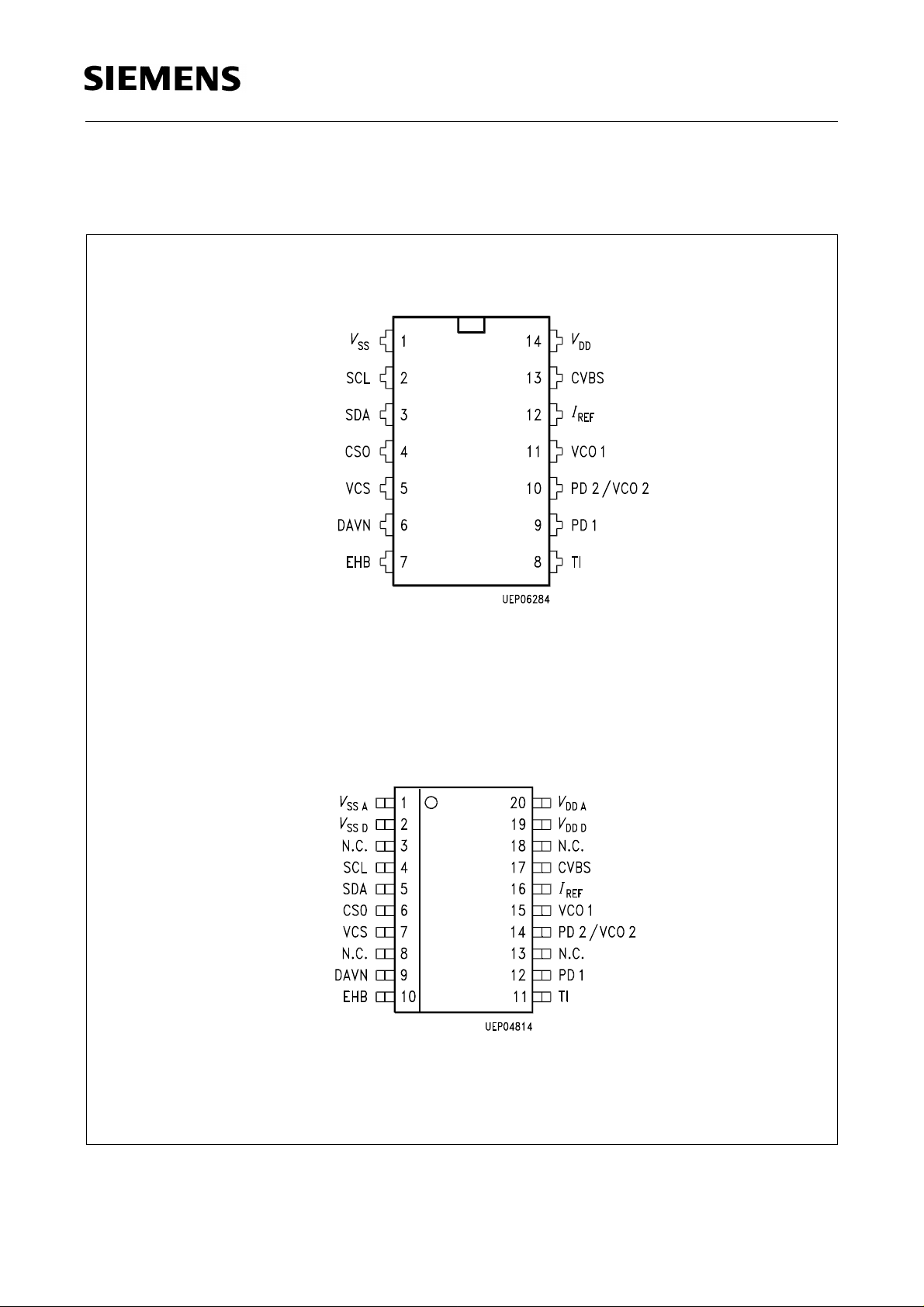
Pin Configuration
(top view)
SDA 5648
SDA 5648X
P-DIP-14-3
P-DSO-20-1
Operating mode (PDC/VPS) is selected by a control register which can be written to via theI
interface.
2
C-Bus
Semiconductor Group 22
Pin Definitions and Functions
SDA 5648
SDA 5648X
Pin No.
P-DIP-14-3
1
Pin No.
P-DSO-20-1
1
2
Symbol Function
V
SS
V
SSA
V
SSD
Ground (0 V)
Analog ground (0 V)
Digital ground (0 V)
3 N.C. Not connected
2 4 SCL Serial clock input of I
3 5 SDA Serial data input of I
4 6 CS0 Chip select input determining the I
2
C-Bus.
2
C-Bus.
2
C-Bus addresses:
20H / 21H, when pulled low
22H / 23H, when pulled high.
5 7 VCS Video Composite Sync output from sync slicer used for
PLL based clock generation.
8 N.C. Not connected
6 9 DAVN Data available output active low, when PDC/VPS data
is received.
7 10 EHB Output signaling the presence of the first field active
high.
8 11 TI Test input; activates test mode when pulled high.
9 12 PD1 Phase detector/charge pump output of data PLL
(DAPLL).
13 N.C. Not connected
10 14 PD2/VCO2 Connector of the loop filter for the SYSPLL.
11 15 VCO1 Input to the voltage controlled oscillator #1 of the
DAPLL.
12 16
I
REF
Reference current input for the on-chip analog circuit.
13 17 CVBS Composite video signal input.
18 N.C. Not connected
14
19
V
DD
V
DDD
Positive supply voltage (+ 5 V nom.).
Positive supply voltage for the digital circuits
(+ 5 V nom.).
20
V
DDA
Positive supply voltage for the analog circuits
(+ 5 V nom.).
Semiconductor Group 23

SDA 5648
SDA 5648X
Block Diagram
Semiconductor Group 24

SDA 5648
SDA 5648X
Circuit Description
Referring to the functional block diagram of the PDC / VPS decoder, the composite video signal with
negative going sync pulses is coupled to the pin CVBS through a capacitor which is used for
clamping the bottom of the sync pulses to an internally fixed level. The signal is passed on to the
slicer, an analog circuitry separating the sync and the data parts of the CVBS signal, thus yielding
the digital composite sync signal VCS and a digital data signal for further processing by comparing
those signals to internally generated slicing levels.
The output of the sync separator is forwarded, on one hand, to the output pin VCS, and on the other
hand, to the clock generator and the Timing block. The VCS signal represents a key signal that is
used for deriving a system clock signal by means of a PLL.
The data slicer separates the data signal from the CVBS signal by comparing the video voltage to
an internally generated slicing level which is found by averaging the data signal during TV line no.
16 in the VPS mode or by averaging the data signal during the clock run-in period of the teletext
lines during the data entry window (DEW) in PDC mode.
The clock generator delivers the system clock needed for the basic timing as well as for the
regeneration of the data clock. It is based on two phase locked loops (PLL’s) all parts of which are
integrated on chip with the exception of the loop filter components. Each of the PLL’s is composed
of a voltage controlled oscillator (VCO), a phase/frequency detector (PFD), and a charge pump
which converts the digital output signals of the PFD to an analog current. That current is
transformed to a control voltage for the VCO by the off-chip loop filter. The generated VCO frequencies are 10 MHz and 13.875 MHz for VPS mode and PDC mode, respectively.
All signals necessary for the control of sync and data slicing as well as for the data acquisition are
generated by the Timing block.
In PDC mode, only teletext rows 8/30 containing Broadcast Data Service Package (BDSP) information are acquired. The relevant bytes of 8/30 format 1 (8/30/1) and 8/30 format 2 (8/30/2) are
extracted. The 8/30/1-bytes are stored in the acquisition register in a transparent way without any
bit manipulation, whereas the Hamming coded bytes of packet 8/30/2 are Hamming-checked and
bytes with one bit error are corrected. The storage of error free or corrected 8/30/2-data bytes in the
transfer register to the I2C-Bus is signalled by the DAVN output going low. The reception and
storage of 8/30/1- data, however, is not indicated by the DAVN output. The presence of 8/30/1 data
can only be checked by polling the data register via the I2C-Bus.
In VPS mode, the extracted data bits of TV line no. 16 are checked for biphase errors. With no
biphase errors encountered, the acquired bytes are stored in the transfer register to the I2C-Bus.
That transfer is signalled by a H/L transition of the DAVN output, as well.
In both operating modes data are updated when a new data line has been received, provided that
the chip is not accessed via the I2C-Bus at the same time.
A micro controller can read the stored bytes via the I2C-Bus interface at any time. However, one
must be aware that the storage of new data from the acquisition interface is inhibited as long as the
PDC decoder is being accessed via the I2C-Bus. At the end of an I2C-Bus reading the transfer
registers are set to FF (hex) until they are updated by the reception of new data packet contained
in the CVBS signal.
Semiconductor Group 25

SDA 5648
SDA 5648X
I2C-Bus
General Information
The I2C-Bus interface implemented on the PDC decoder is a slave transmitter/receiver, i.e., both
reading from and writing to the PDC / VPS decoder is possible. The clock line SCL is controlled only
by the bus master usually being a micro controller, whereas the SDA line is controlled either by the
master or by the slave. A data transfer can only be initiated by the bus master when the bus is free,
i.e., both SDA and SCL lines are in a high state. As a general rule for the I2C-Bus, the SDA line
changes state only when the SCL line is low. The only exception to that rule are the Start Condition
and the Stop Condition. Further details are given below. The following abbreviations are used:
START : Start Condition generated by master
AS : Ackknowledge by slave
AM : Ackknowledge by master
NAM : No Ackknowledge by master
STOP : Stop Condition generated by master
Chip Address
There are two pairs of chip addresses, which are selected by the CS0-input pin according to the
following table
CS0 Input Write Mode Read Mode
Low 20 (hex) 21 (hex)
High 22 (hex) 23 (hex)
Write Mode
For writing to the PDC decoder, the following format has to be used:
START Chipadress White Mode AS Byte Set Control Register AS STOP
Data Transfer (Write Mode)
Step1
: In order to start a data transfer the master generates a Start Condition on the bus by pulling
the SDA line low while the SCL line is held high.
Step 2
Step 3
: The bus master puts the chip address on the SDA line during the next eight SCL pulses.
: The master releases the SDA line during the ninth clock pulse. Thus the slave can generate
an acknowledge (AS) by pulling the SDA line to a low level.
Step 4
Step 5
Step 6
The write mode is used to set the I2C-Bus control register which determines the operating mode:
Semiconductor Group 26
: The controller transmits the data byte to set the Control register.
: The slave acknowledges the reception of the byte.
: The master concludes the data communication by generating a Stop Condition.

SDA 5648
SDA 5648X
Control Register
Bit Number 7 6 5 4 3 2 1 0
T4 T3 T2 T1 T0 DIS PDC/
VPS
Default: All bits are set to 0 on power-up.
Bit 0: Determines, which kind of data is accessed via the I2C-Bus when PDC mode is active.
Value
01
BDSP
8/ 30/ 2
data accessible
Bit 1: Determines the operating mode.
01
VPS mode active PDC mode active
BDSP 8/ 30/ 1 or
header row
data accessible (refer to description of Bit 2)
Value
FOR1/
FOR2
Bits 2 through 7 are used for test purposes.
DIS: Don‘t care.
Bits 3 through 7 must not be changed for normal operation by user software!
Read Mode
For reading from the PDC decoder, the following format has to be used.
START Chipaddress Read Mode AS 1st Byte AM … Last
Byte
NAM STOP
Semiconductor Group 27
 Loading...