

Siemens PSB7280 Datasheet

ICs for Communications
Joint Audio Decoder-Encoder
PSB 7280 Version 3.1
Data Sheet 1998-07-01
DS 1

PSB 7280
Revision History: Current Version: 1998-07-01
Previous Version: Preliminary Data Sheet 06.96 (V 2.2)
Page
(in previous
Version)
Page
(in current
Version)
Subjects (major changes since last revision)
For questions on technology, delivery and prices please con tact the Semicon ductor Group Of fices
in Germany or the Siemens Companies and Representatives worldwide: see our webpage at
http://www.siemens.de/semiconductor/communication
IOM®, IOM®-1, IOM®-2, SICOFI®, SICOFI®-2, SICOFI®-4, SICOFI®-4µC, SLICOFI®, ARCOFI
ARCOFI
SICAT
MUSAC
®
-SP, EPIC®-1, EPIC®-S, ELIC®, IPAT®-2, ITAC®, ISAC®-S, ISAC®-S TE, ISAC®-P, ISAC®-P TE, IDEC®,
®
, OCTAT®-P, QUAT®-S are registered trademarks of Siem ens AG.
™
-A, FALC™54, IWE™, SARE™, UTPT™, ASM™, ASP™, DigiTape™ are trademarks of Siemens AG.
®
, ARCOFI®-BA,
Edition 1998-07-01
Published by Siemens AG,
HL SP,
Balanstraße 73,
81541 München
© Siemens AG 1998.
All Rights Reserved.
Attention please!
As far as patents or other rights of third parties are concerned, liability is only assumed for components, not for
applications, processes and c irc uit s imp lemented within componen ts or as s em blies.
The information describe s the t yp e of co m ponent and shall not be considered as assured characteristics .
Terms of delivery and rights to ch ange design reserved.
Due to technical requireme nt s com ponents may contain dange rous substances. For informa tio n on t he t y pes in
question please contact yo ur nearest Siemens Office, Semic onductor Group.
Siemens AG is an approved CECC manufacturer.
Packing
Please use the recycling ope rat ors k now n t o y ou. W e ca n als o help you – get in touch with your neares t sa les
office. By agreement we will take packing material back, if it is sorted. You must bear the costs of transport.
For packing material that is returned to us unsorted or which we are not obliged to accept, we shall have to invoice
you for any costs incurred.
Components used in life-support devices or systems must be expressly authorized for such purpose!
Critical components
systems
2
with the express written approv al of the Semiconductor Group of Siem ens AG.
1 A critical component is a component used in a life-support device or system whose failure can reasonably be
expected to cause the failure of that life-support device or system, or to affect its safety or effectiveness of that
device or system.
2 Life support devices or systems are intended (a) to be implanted in the human body, or (b) to support and/or
maintain and sustain human life. If th ey fail, it is rea so nable to assume that the health of th e us er m ay be endangered.
1
of the Semiconductor Group of Siemens AG, may only be used in life -s upport devices or

PSB 7280
Table of Contents Page
1 Introduction . . . . . . . . . . . . . . . . . . . . . . . . . . . . . . . . . . . . . . . . . . . . . . . . 5
1.1 Overview . . . . . . . . . . . . . . . . . . . . . . . . . . . . . . . . . . . . . . . . . . . . . . . . . . . 5
1.2 Feature List . . . . . . . . . . . . . . . . . . . . . . . . . . . . . . . . . . . . . . . . . . . . . . . . . 7
1.3 Logic Symbol . . . . . . . . . . . . . . . . . . . . . . . . . . . . . . . . . . . . . . . . . . . . . . . . 9
1.4 Pin Configuration . . . . . . . . . . . . . . . . . . . . . . . . . . . . . . . . . . . . . . . . . . . . 10
1.5 Pin Description . . . . . . . . . . . . . . . . . . . . . . . . . . . . . . . . . . . . . . . . . . . . . . 11
1.6 Functional Block Diagram . . . . . . . . . . . . . . . . . . . . . . . . . . . . . . . . . . . . . 17
1.7 System Integration . . . . . . . . . . . . . . . . . . . . . . . . . . . . . . . . . . . . . . . . . . . 18
2 General Architecture and Functions . . . . . . . . . . . . . . . . . . . . . . . . . . . 21
2.1 Architecture . . . . . . . . . . . . . . . . . . . . . . . . . . . . . . . . . . . . . . . . . . . . . . . . 21
2.2 Functions . . . . . . . . . . . . . . . . . . . . . . . . . . . . . . . . . . . . . . . . . . . . . . . . . . 22
2.2.1 Summary of the Functions . . . . . . . . . . . . . . . . . . . . . . . . . . . . . . . . . . . 22
2.2.2 Audio Functions and Supplementary Features . . . . . . . . . . . . . . . . . . . 23
3 Interfaces and Memory Organization . . . . . . . . . . . . . . . . . . . . . . . . . . . 24
3.1 Interfaces . . . . . . . . . . . . . . . . . . . . . . . . . . . . . . . . . . . . . . . . . . . . . . . . . . 24
®
3.1.1 IOM
-2 Interface . . . . . . . . . . . . . . . . . . . . . . . . . . . . . . . . . . . . . . . . . . 24
3.1.2 Serial Audio Interface . . . . . . . . . . . . . . . . . . . . . . . . . . . . . . . . . . . . . . 26
3.1.3 Parallel Host Interface . . . . . . . . . . . . . . . . . . . . . . . . . . . . . . . . . . . . . . 28
3.1.4 External Memory Interface . . . . . . . . . . . . . . . . . . . . . . . . . . . . . . . . . . . 28
3.1.5 Clock Interface . . . . . . . . . . . . . . . . . . . . . . . . . . . . . . . . . . . . . . . . . . . . 29
3.2 Shared Memories . . . . . . . . . . . . . . . . . . . . . . . . . . . . . . . . . . . . . . . . . . . 29
3.3 Directly Accessible Register Bank . . . . . . . . . . . . . . . . . . . . . . . . . . . . . . . 31
3.3.1 Input/Output Registers . . . . . . . . . . . . . . . . . . . . . . . . . . . . . . . . . . . . . . 31
3.3.2 DSP/Host Com Area with a Multiplexed Host Interface . . . . . . . . . . . . . 35
3.3.2.1 Access to DSP/Host Com Area . . . . . . . . . . . . . . . . . . . . . . . . . . . . . 35
3.3.2.2 Mailbox . . . . . . . . . . . . . . . . . . . . . . . . . . . . . . . . . . . . . . . . . . . . . . . 40
3.3.3 DSP/Host Com Area with a Demultiplexed Host Interface . . . . . . . . . . 43
4 Functional Blocks . . . . . . . . . . . . . . . . . . . . . . . . . . . . . . . . . . . . . . . . . . 47
4.1 PLL and Baud Rate Generator . . . . . . . . . . . . . . . . . . . . . . . . . . . . . . . . . 47
4.2 Audio and Data Reception/Transmission . . . . . . . . . . . . . . . . . . . . . . . . . 50
4.3 HDLC Controller . . . . . . . . . . . . . . . . . . . . . . . . . . . . . . . . . . . . . . . . . . . . 63
®
4.4 IOM
-2 Functions . . . . . . . . . . . . . . . . . . . . . . . . . . . . . . . . . . . . . . . . . . . 72
4.4.1 Monitor Channel Protocol . . . . . . . . . . . . . . . . . . . . . . . . . . . . . . . . . . . 73
4.4.2 C/I Channel . . . . . . . . . . . . . . . . . . . . . . . . . . . . . . . . . . . . . . . . . . . . . . 79
4.5 Programming Indirectly Accessible Registers . . . . . . . . . . . . . . . . . . . . . . 83
4.5.1 Programming via Parallel Host Interface . . . . . . . . . . . . . . . . . . . . . . . . 83
Semiconductor Group 3 Data Sheet1998-07-01

PSB 7280
Table of Contents Page
5 Register Description . . . . . . . . . . . . . . . . . . . . . . . . . . . . . . . . . . . . . . . . 84
5.1 Interrupt Structure . . . . . . . . . . . . . . . . . . . . . . . . . . . . . . . . . . . . . . . . . . . 84
5.2 Interrupt Status Registers . . . . . . . . . . . . . . . . . . . . . . . . . . . . . . . . . . . . . 85
5.3 Indirectly Accessible Configuration and Control Registers . . . . . . . . . . . . 89
5.4 HDLC Controller Registers . . . . . . . . . . . . . . . . . . . . . . . . . . . . . . . . . . . 115
6 Firmware Features . . . . . . . . . . . . . . . . . . . . . . . . . . . . . . . . . . . . . . . . . 132
6.1 Basic Functions . . . . . . . . . . . . . . . . . . . . . . . . . . . . . . . . . . . . . . . . . . . . 132
6.1.1 Firmware Version Number . . . . . . . . . . . . . . . . . . . . . . . . . . . . . . . . . . 132
6.1.2 Software Reset . . . . . . . . . . . . . . . . . . . . . . . . . . . . . . . . . . . . . . . . . . 134
6.1.3 Power Down Command . . . . . . . . . . . . . . . . . . . . . . . . . . . . . . . . . . . . 135
6.2 Audio Interfaces . . . . . . . . . . . . . . . . . . . . . . . . . . . . . . . . . . . . . . . . . . . . 136
6.2.1 Compressed Audio Protocols and Control of JADE . . . . . . . . . . . . . . 138
6.2.1.1 Outband Control of JADE . . . . . . . . . . . . . . . . . . . . . . . . . . . . . . . . 138
6.2.1.2 Compressed Audio Protocol with Outband Control . . . . . . . . . . . . . 149
6.2.1.3 Compressed Audio Protocol with Inband Control . . . . . . . . . . . . . . 149
6.2.2 Uncompressed Data Protocol . . . . . . . . . . . . . . . . . . . . . . . . . . . . . . . 157
6.2.3 Audio Interface Timings . . . . . . . . . . . . . . . . . . . . . . . . . . . . . . . . . . . . 157
6.2.3.1 Uncompressed Data: Host IF
Compressed Data: Host IF. . . . . . . . . . . . . . . . . . . . . . . . . . . . . . . . 157
6.2.3.2 Uncompressed Data: IOM IF
Compressed Data: Host IF. . . . . . . . . . . . . . . . . . . . . . . . . . . . . . . . 165
6.2.3.3 Uncompressed Data: IOM IF
Compressed Data: Serial Audio Interface (SAI). . . . . . . . . . . . . . . . 174
7 Electrical Specification . . . . . . . . . . . . . . . . . . . . . . . . . . . . . . . . . . . . . 176
7.1 Absolute Maximum Ratings . . . . . . . . . . . . . . . . . . . . . . . . . . . . . . . . . . . 176
7.2 Operating Conditions . . . . . . . . . . . . . . . . . . . . . . . . . . . . . . . . . . . . . . . . 176
7.3 DC Characteristics . . . . . . . . . . . . . . . . . . . . . . . . . . . . . . . . . . . . . . . . . . 177
7.4 Capacitances . . . . . . . . . . . . . . . . . . . . . . . . . . . . . . . . . . . . . . . . . . . . . . 178
7.5 Oscillator Circuit . . . . . . . . . . . . . . . . . . . . . . . . . . . . . . . . . . . . . . . . . . . . 178
7.6 XTAL 1,2 Recommended Typical Crystal Parameters . . . . . . . . . . . . . . 179
7.7 AC Characteristics . . . . . . . . . . . . . . . . . . . . . . . . . . . . . . . . . . . . . . . . . . 179
7.7.1 Testing Waveform . . . . . . . . . . . . . . . . . . . . . . . . . . . . . . . . . . . . . . . . 179
7.7.2 Parallel Host Interface Timing . . . . . . . . . . . . . . . . . . . . . . . . . . . . . . . 180
®
7.7.3 IOM
-2 Interface Timing . . . . . . . . . . . . . . . . . . . . . . . . . . . . . . . . . . . 184
7.7.4 Serial Audio Interface Timing . . . . . . . . . . . . . . . . . . . . . . . . . . . . . . . . 186
7.7.5 External Memory Interface . . . . . . . . . . . . . . . . . . . . . . . . . . . . . . . . . . 189
8 Package Outline . . . . . . . . . . . . . . . . . . . . . . . . . . . . . . . . . . . . . . . . . . . 190
Semiconductor Group 4 Data Sheet1998-07-01

PSB 7280
1 Introduction
1.1 Overview
The PSB 7280 Joint Audio Decoder Encoder is a device which implements voice
compression algorithms using the Low-Delay Code Excited Linear Prediction (LD-CELP)
standard as defined in the ITU-T G.728 Recommendation, and for 7-kHz voice using the
Sub-Band Coded Adaptive Differential PCM (SBC-ADPCM) coding according to the
G.722 Recommendation. In addition G.711 PCM audio coding is also supported.
Thus in the G.728 mode it compres ses a dig itized PC M (64 kbit /s) or linear (12 8 kbit/s )
voice signal into a 16 kbit/s bit stream, and vice v ersa . The algorithm is implemente d in
16-bit fixed point a rithmetic and complies with the newest fixed point specification set
forth by the ITU.
In the G.722 mode it compresses the PCM compressed (128 kbit/s) or the linear
uncompressed (256 kbit/s) 7 kHz audio samples in to a rate o f 48/56/6 4 kbit/s , and v ice
versa.
The JADE finds applications in
– ISDN Videophones (H.320)
– Vid eo Conf eren ce Syst ems
– Corporate Network voice concentrators, multiplexers and gateways
– Data-over-voice and Voice-over-data terminals.
Other potential application areas are:
– Networks (e.g. LANs) for packetized voice
– Digital Added Main-Line (DAML) & Digital Circuit Multiplication Equipment (DCME)
– Voice storage e.g. in PC based applications
– Message recording and distribution.
The interfaces of the JADE allow a seamless integration into IOM-2 based systems.
After the circuit is set up in the proper mode o f operation and parameter settin gs are
programmed by a controlling soft ware, the circuit runs in dependently of the rest of the
system. Status and control information to/from the JADE can be transferred either
inband the compressed audio data via the corresp onding sel ect ed interf ace or outband
using an 8-bit parallel host interface.
In a Videophone system using the 8 × 8 (formerly IIT) VCP (Video Codec and Multimedia
Communications Processor) th e Siemens PSB 7280 can work standalone wi thout the
need of external initialization. The default configuration of the JADE is such, that no host
is needed in this case and the fu ll communication is done between the VCP and the
Siemens PSB 7280.
The voice compression algorith ms are implem ented by an embedd ed 16-bit fixed point
Digital Signal Processor with all memories internal and no external memory needed.
Semiconductor Group 5 Data Sheet 1998-07-01

PSB 7280
Integration of these and other features, as well as perfectly matched interfaces with other
ICs allows for the implementation of highly optimized, low cost system solutions e.g. for
Videophones, Data-over-voice and Channel Multiplexing equipment.
For system integration, two serial HDLC/transparent data channels are implemented
which can be serviced by an attached hos t (or th e on-chip DSP). Syst em functions and
communication between the chip and an external controller is supported by a full-duplex
256-byte on-chip mailbox communication memory.
The circuit is offered in a Quad Flat Pack package with 100 pins (P-TQFP-100: size
14 ×14 mm, pitch 0.5 mm, height 1.4 mm).
Note: This Data Sheet gives a thorough d escription of the func tions and hardware th at
forms the base of PSB 7280. It includes information (e.g. External Memory
“
Interface) that is not needed for the PSB 7280 as a
G.728/G.722/G.711 audio compression device.
ready to use plug and play
”
Semiconductor Group 6 Data Sheet 1998-07-01
Joint Audio Decoder-Encoder
PSB 7280
Version 3.1 CMOS
1.2 Feature List
Functions
– G.728 compression/decompression (16 kbit/s)
– G.722 compres sio n/d eco mpres si on for 7-k Hz aud io
(64, 56, 48 kbit/s)
– G.711 compression/decompression (64 kbit/s)
– Digital sampling rate conversion (16 kHz - 8 kHz) for
G.722 audio with 8-kHz C odec (ban dwidth red uced
to 3.4 kHz)
– Accepts/outputs uncompressed audio in 8-bit PCM A/µ law or 16-bit linear format
– Uncompressed/compressed audio switchable between different interface
combinations (IOM/Serial Audio Interface, IOM/Host, Host/Host)
– Inband controlled H.221/H.223 oriented audio protocol, e.g. for direct serial
connection to vide ocodec (VCP of 8 × 8 Inc., formerl y IIT Inc .) as well as hos t based
solutions
– Outband controlled audio protocol with optimized data rate
– Stable reaction on interrupt handshake timing violations of e.g. a slow host
®
(Windows
PC)
P-TQFP-100
System On-chip Functions
– Two universal serial HDLC/transparent data controllers
– IOM-2 monitor and C/I channels
– Generation of programmable system clock output
– Three programmable timers
– Programmable on-chip PLL for internal clock generation from ISDN low frequency
(7.68 MHz) clock
Type Ordering Code Package
PSB 7280 Q67101-H6773 P-TQFP-100
Semiconductor Group 7 Data Sheet 1998-07-01

PSB 7280
Interfaces
– 4-line IOM-2/PCM interface
– 5-line serial audio interface, e.g. for connection to videocodec/H.221/223 processor
– Parallel 8-bit Host interface
– 4-line general purpose interface
– External memory interface to external SRAM with programmable waitstates (0 to 15),
for devel opment purposes only.
Control
– Programmable via parallel host interface
– Operating parameters and mode settings via a register bank
– Access to audio channel s and H DLC/seria l transpa rent data c ontrollers from DSP or
an external host
– Interface to external software via a full-duplex 256-byte on-chip mailbox
– H.221/H.223 oriented inband configuration/mode switching
General
– Supply voltage: 3.0 - 3.6 V
– Additional 4.5 to 5.5 V supply for connection to 5-V systems without external
components
– Ambient temperature range 0 °C to + 70 °C
– P-TQFP-100 package
Semiconductor Group 8 Data Sheet 1998-07-01
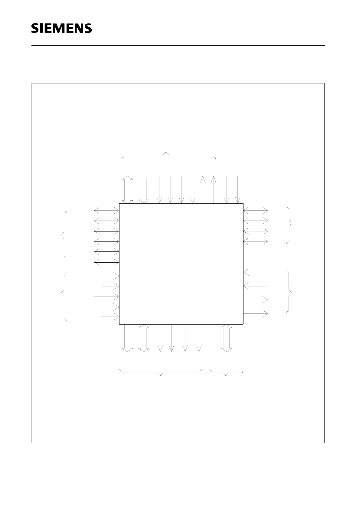
1.3 Logic Symbol
Paral lel Host Interf ace
RD#
WR#
A(0:3)
(R/W#)
(DS#)
CS#
ALE
PSB 7280
INT#AD(0:7)
RESET
EA #INTR#
Serial
Audio
Interface
Power
Suppl y
SIO
SCLK
SR
ST
RFS
TFS
VDD
VDDP, VDDAP
VS S
VDDA
VSSA, VSSAP
PSB 7280
CA(0:15) CD(0:15)
Exter nal Mem o r y Inte r fa ce
CRD#
CWR#
CPS#
CDS#
GP IO Interface
GPIO(0:3)
DD
DU
DCL
FSC
CM1
XTAL1
XTAL2
CLKO
IOM-2
Int erfa ce
System
Clock
Interface
Figure 1
Semiconductor Group 9 Data Sheet 1998-07-01
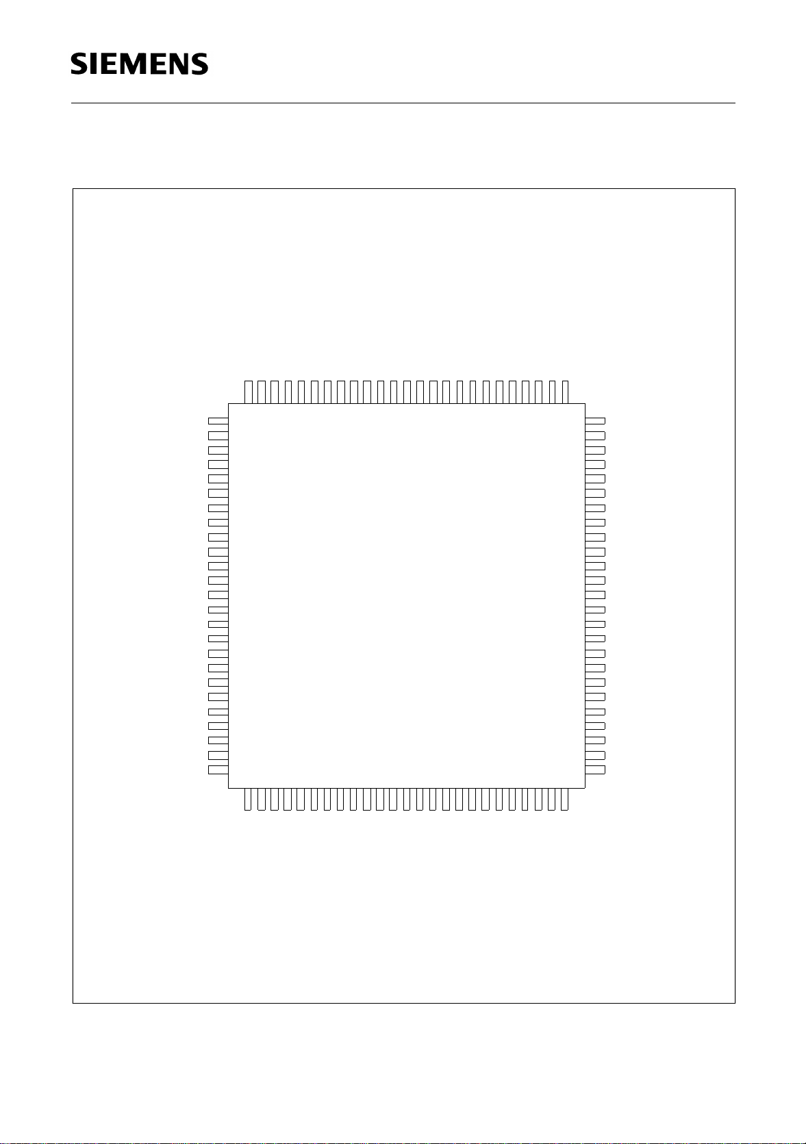
1.4 Pin Configuration
SRSTRFS
TFSA3CM1
PSB 7280
VSS
VDD
VSSA
XTAL2
XTAL1
VDDA
VSSAP
VDDAP
CLKO
SIO
RES ETA1A0
GP3
GP2
GP1
GP0
VSS
CD0
SCLK
ALE
CS#
RD#
WR#
AD7
AD6
AD5
AD4
VDDP
VSS
VDD
AD3
AD2
AD1
AD0
INTR#
INT#
A2
FSC
DCL
DU
DD
CA1 5
CD15
1
PSB 7280
P-TQFP-100
26
76
51
CA0
CD1
CA1
VSS
VDDP
CD2
CA2
CD3
CA3
VSS
VDD
CD4
CA4
CD5
CA5
VDD
VSS
VDD
CD6
CA6
CD7
CA7
VSS
VDD
CD8
CA14
CD14
VDD P
VSS
CA13
CD13
CA12
CD12
VDD
VSS
VDD
CA11
CD11
CA10
CD10
VDD
VSS
EA#
CDS#
CPS#
CWR#
CRD#
CA9
CD9
CA8
Figure 2
Semiconductor Group 10 Data Sheet 1998-07-01

PSB 7280
1.5 Pin Description
Table 1 Parallel Host Interface
Pin No. Symbol Function Descriptions
16 AD0 I/O Multiplexed Bus Mode: Address/Data Bus. Transfers
15 AD1 I/O
14 AD2 I/O
13 AD3 I/O
9 AD4 I/O
8 AD5 I/O
7 AD6 I/O
6 AD7 I/O
addresses from the host to JADE and data between the
host and the JADE
Demultiplexed Bus Mode: Data bus. Transfers data
between the host and the JADE
4DS
RD
5R/W
WR
3CS
2 ALE I Address Latch Enable.
I Data Strobe.
The rising edge marks the end of a valid read or write
operation (Motorola bus mode).
I Read.
This signal indicates a read operation (Siemens/Intel
bus mode).
I Read/Write.
A 1 (“high“) identifies a valid host access as a read
operation. A 0 identifies a valid host access as a write
operation (Motorola bus mode)
IWrite.
This signal indicates a write operation (Siemens/Intel
bus mode).
I Chip Select.
A “high” on this line indicates an address on AD(0:7)
(multipexed bus mode only). ALE also selects the
interface mode
82 A0 I Address Bits A(0:3) (demultiplexed bus type)
83 A1 I
19 A2 I
96 A3 I
Semiconductor Group 11 Data Sheet 1998-07-01
Table 1 Parallel Host Interface (cont’d)
Pin No. Symbol Function Descriptions
17 INTR O (OD) Interrupt Real-time.
Interrupt output line for high priority interrupt status
(serial audio receive/transmit, serial HDLC data
receive/transmit data) to host.
PSB 7280
18 INT
O (OD) Interrupt Request.
Interrupt output line for all other interrupt states.
®
Table 2 IOM
-2 Interface
Pin No. Symbol Function Descriptions
23 DD I/O(OD) Data Downstream on IOM-2/PCM interface.
22 DU I/O(OD) Data Upstream on IOM-2/PCM interface.
21 DCL I/O(OD) Data Clock.
Clock frequency is twice the data rate, or equal to the
data rate.
20 FSC I/O(OD) Frame Sync.
Marks the beginning of a physical IOM-2 or PCM frame.
Table 3 Serial Audio Interface
Pin No. Symbol Function Descriptions
1 SCLK I/O Serial Clock.
Serial clock for SR and ST.
100 SR I/O(OD) Serial Data Receive.
V
Should be connected to
via a pulld own resistor if not
SS
used.
99 ST I/O( OD) Serial Data Transmit.
98 RFS I/O Audio Receive Frame Sync.
97 TFS I/O Audio Transmit Frame Sync.
Semiconductor Group 12 Data Sheet 1998-07-01

Table 4 System Clocks
Pin No. Symbol Function Descriptions
90 XTAL1 I Crystal In or Clock In.
If a crystal is used, it is connected between XTAL1 and
XTAL2. If a clock signal is provided (via an external
oscillator), this signal is input via XTAL1. In this case the
XTAL2 output is to be left non-connected. The XTAL1
input has to be 50% duty cycle and must not exceed the
voltage range between
91 XTAL2 O Crystal Out.
Left unconnected if a crystal is not used.
86 CLKO O Clock Out.
Output clock of frequency equal to the internal
frequency divided by a programmable factor.
V
SSA
and V
DDA
PSB 7280
.
Table 5 External Memory Interface (for Development Purposes only)
Pin No. Symbol Function Descriptions
75 CA0 O C-Bus Address.
73 CA1 O Used for addressing ROM or RAM external to the chip.
69 CA2 O Is to be left NC if not used.
67 CA3 O
63 CA4 O
61 CA5 O
56 CA6 O
54 CA7 O
50 CA8 O
48 CA9 O
39 CA10 O
37 CA11 O
32 CA12 O
30 CA13 O
26 CA14 O
24 CA15 O
Semiconductor Group 13 Data Sheet 1998-07-01
PSB 7280
Table 5 External Memory Interface (for Development Purposes only) (cont’d)
Pin No. Symbol Function Descriptions
76 CD0 I/O C-Bus Data.
74 CD1 I/O
70 CD2 I/O
68 CD3 I/O
64 CD4 I/O
62 CD5 I/O
57 CD6 I/O
55 CD7 I/O
51 CD8 I/O
Data bus for external ROM or RAM. Is to be left NC if not
used.
49 CD9 I/O
40 CD10 I/O
38 CD11 I/O
33 CD12 I/O
31 CD13 I/O
27 CD14 I/O
25 CD15 I/O
43 EA
47 CRD
I External program Access enable
O C-Bus Read to external memories.
When “high”, an access to program address range
(0000
ROM. Access to 8000
-7FFFH) fetches an instruction from on-chip
H
-FFFFH addresses external
H
memory via the External Memory Interface.
When “low”, an access to 0000
0000
-7FFFH, normally reserved for on-chip software)
H
-FFFFH (including
H
accesses external program memory via the External
Memory Interface.
Left NC if not used.
46 CWR
O C-Bus Write to external memories.
Left NC if not used.
45 CPS
O C-Bus Select line for external program memory.
Left NC if not used.
44 CDS
O C-Bus Select line for external data memory.
Left NC if not used.
Semiconductor Group 14 Data Sheet 1998-07-01
Table 6 General Control
Pin No. Symbol Function Descriptions
95 CM1 I Clock Mode
Selects the option for the generation of the DSP internal
working clock.
85 SIO I/O Serial I/O line.
When programmed as input, a rising or falling
(selectable) edge on this line may generate a maskable
interrupt INT
(host) or INT1 (DSP).
When programmed as output, its state is directly
controlled by the DSP or the host.
84 RESET I Reset input. Reset time: > 1 ms.
Table 7 General Purpose I/O Interface
PSB 7280
Pin No. Symbol Function Descriptions
81 GP0 I/O (OD) General purpose I/O pins
80 GP1 I/O (OD)
79 GP2 I/O (OD)
78 GP3 I/O (OD)
Semiconductor Group 15 Data Sheet 1998-07-01
Table 8 Power Supply
Pin No. Symbol Function Descriptions
PSB 7280
11
29
35
42
53
59
66
72
77
94
12
36
60
93
34
V
V
V
V
V
V
V
V
V
V
V
V
V
V
V
41 V
52
V
SS
SS
SS
SS
SS
SS
SS
SS
SS
SS
DD
DD
DD
DD
DD
DD
DD
I Ground (common to VDD and V
DDP
) .
I
I
I
I
I
I
I
I
I
I Positive power supply voltage (3.0 - 3.6 V).
I
I
I
I
I
I
Note: In former versions, pins 34, 41, 52, 58 and 65
V
could be connected to
them to be connected to
. This version requires
DDP
V
.
DD
58
65
10
28
71
89
92
87
V
V
V
V
V
V
V
V
88 V
DD
DD
DDP
DDP
DDP
DDA
SSA
DDAP
SSAP
I
I
I Positive power supply voltage (4.5 - 5.5 V) for external
I
interfaces.
I
I Separate positive power supply voltage (3.0 - 3.6 V) for
Clock Generation Unit (Oscillator).
I Separate Ground (0 V) for Clock Generation Unit
(Oscillator).
I Separate positive power supply voltage (3.0 - 3.6 V) for
Clock Generation Unit (PLL).
Note: The power supply for the PLL requires pin 87
connected to
connected to
V
V
. In former versions pin 87 was
DDAP
DDP
I Separate Ground (0 V) for Clock Generation Unit (PLL)
Semiconductor Group 16 Data Sheet 1998-07-01
1.6 Functional Block Diagram
PSB 7280
SCL K
SR
ST
RFS
TFS
Se rial
Audio
I/F
Config/Control
Registers
Tim er s
AD( 0:7) W R#RD# ALE INTR#
A(0:3)
CS#
Parallel Host Inte rface
Audio
Channe ls
Mailbox
Mailb ox
256 byte
256 byte
DSP
Core
RAM ROM
IN T#SIO
HDLC/
Data
Channels
Rese t
EA#
Mon, C/I
Con trol
IOM/
PCM
BRG
clock
gen/
PLL
DD
DU
DCL
FSC
CM1
CLKO
XTA L1
XTA L2
External Memory Interface
C A(0 :15 ) CD(0 :15 ) CWR#CRD#
CPS#
CDS#
Figure 3
Detailed description see Chapter 2.
Semiconductor Group 17 Data Sheet 1998-07-01
PSB 7280
1.7 System Integration
Example of integration in ISDN/analog videophone:
The first example represents a low-cost so lution for a des k-top standa lone video phone
that connects to an ISDN S0 bus (ISDN basic access) or an analog telephone line.
The ISDN basic access consists of two 64 kbit/s so-called B-channels to carry user
information (voice, data,…), and a separate 16 kbit/s D-channel primarily used for
signaling. The video and audio are both compressed so that they are carried, along with
additional control information, in the two B-channels, or 128 kbit/s.
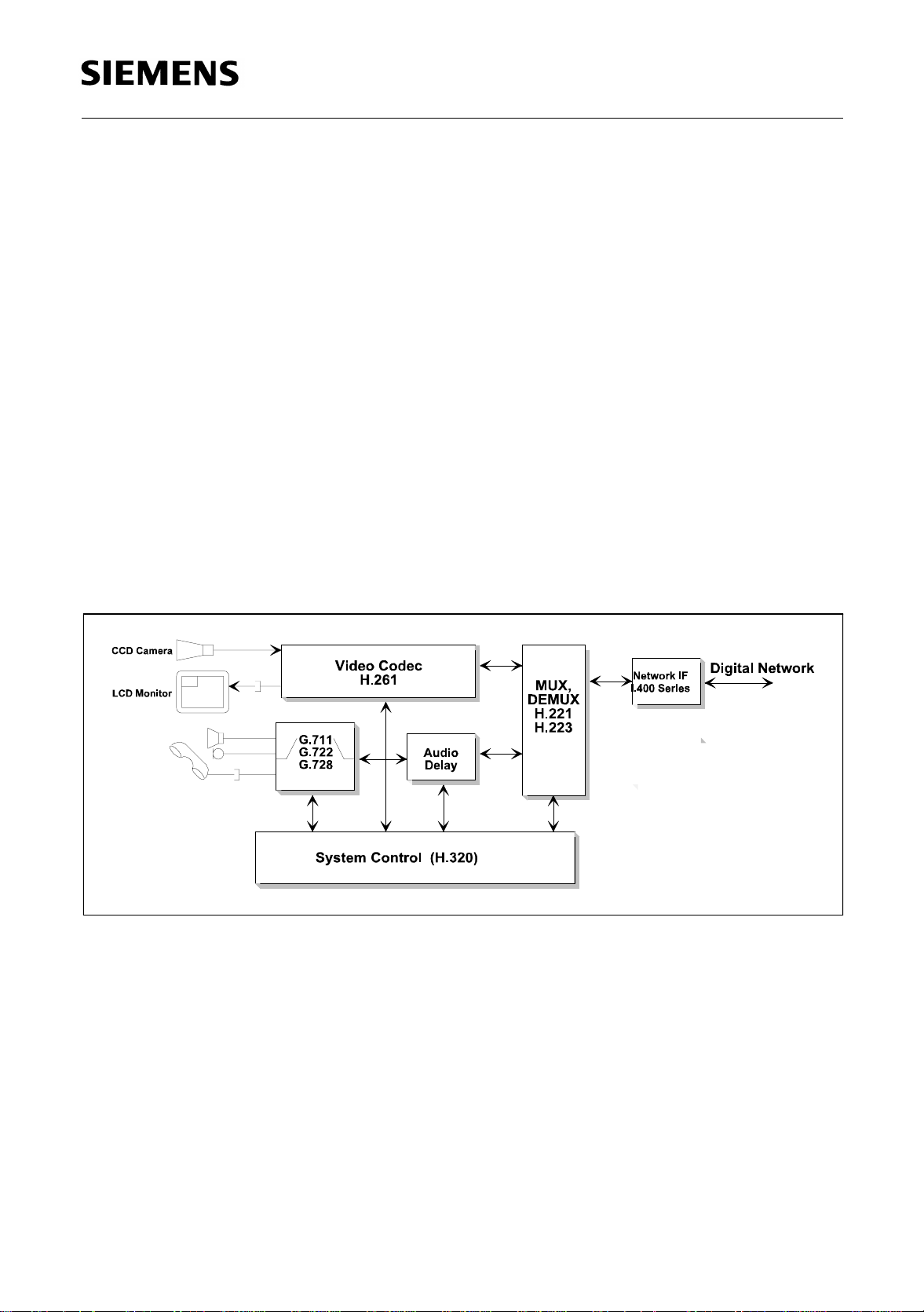
The general aspects of videotel ephony are covered by ITU-T H.320 recomm endation.
The video is compressed according to the H.261 (sometimes called “p × 64”) or the
H.263 recommendation.
For the ISDN videophone (H.320) the compressed video and audio signals are
multiplexed together with additional synchronization and control information into two
B-channels, which are separately switched via the network and thus have to be
resynchronized at the other end. The multiplexing and resynchronization of the
B-channels is specified by the H.221 recommendation (see Figure 4).
F
Figure 4
Using non-parametri c compression techniques, audio can be compressed to 64 kbit/ s
PCM (logarithmical A- or µ-law approximation for 3.1-kHz voice acc. to G.711) or
48/56/64 kbit/s sub-band coded adaptive PCM (for 7-kHz audio acc. to G.722). This
leaves, however, only appro ximate ly 64 kbit/s for video on the ISD N which, at this rat e,
yields only a marginal ly good picture quality. For the ana log videophone it’s not even
possible to transfer only audio at this data rate.
In order to make the best possible use of the total bandwidth and obtain the best possible
video quality, the audio should require only a small fraction of the total data rate. This is
made possible by using parametric compression techniques such as LD-CELP
(16 kbit/s). Above all, the corresponding norms (G.728) are internationally adopted
Semiconductor Group 18 Data Sheet 1998-07-01
PSB 7280
standards, so that compatibility between equipment from different manufacturers is
ensured.
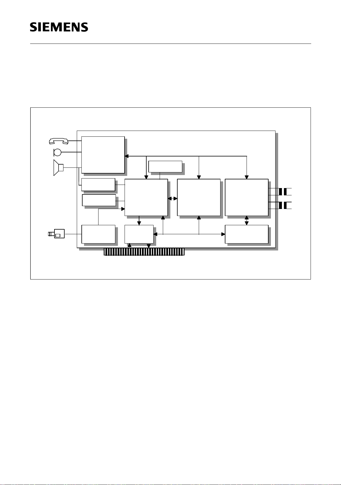
A low-cost H.320 videophon e soluti on fo r ISDN line as a PCI ca rd for comm ercial PC ’s
is shown i n Figure 5.
ARCOFI-SP
SIEMENS
IOM-2
SRAM
JADE
SIEMENS
PSB 7280
Host
ISAC-S TE
SIEMENS
PSB 2186
SIEMENS
SAB 83C515A
ISDN
PAL/NTSC
Camera
PSB 2163
MPEG 1
Stereo DAC
SRAM/DRAM
Video in
Video
Capture
Video
Codec
Video out
PCI
Bus Interface
Figure 5
The JADE and the video c odec chip (e.g. the Video Co mmunication Processor “VCP”
from 8 × 8 Inc.) constitute the heart of the videophone.
Both (together with the microcontroller 83C515) are connected to the PC via the PCI bus
using PCI bus interface (e.g. the “VPIC” of 8 × 8 Inc.).
The JADE compresses/d ecompresses audio accordin g to the ITU-T standards G.728,
G.722 and G.711 and runs a fully inband controlled protocol on the interface to the video
codec. It receives/transmits uncompressed audio via the IOM-2 interface from/to the
ARCOFI-SP. The setup for this application is done automatically after a hardware reset,
so no additional initializa tion by a hos t is req uired . Since the JADE has all its memo ries
on chip, no external SRAM needs to be connected.
The ARCOFI-SP (Audio Ringing Co dec Filter) is a hand s-free codec for 3.1-kH z voice
which performs detection and elaborate balancing of the received and transmitted audio
to suppress undesirable effects due to acoustical feedback of the signal from the remote
subscriber. The quality obtained is very close to that of echo-free full duplex
conferencing.
Semiconductor Group 19 Data Sheet 1998-07-01

PSB 7280
The video is captured by a PAL/NTSC camera and digitized and demodulated e.g. by a
standard SAA 7110 which is directly connected to the video processor. Al ternatively, a
digital camera may be used, which can be connected directly to the video processor.
The video processor compresses and decompresses video according to the ITU-T
standards H.261 and multiplexes/demultiplexes video, audio and data according to
H.221/223. The video processo r uses DRAMs and SRAMs to store data and program
code.
When operating in the ISDN mode, the H.221 multiplexed data stream is sent via the two
B-channels of the IOM-2 interface to the ISAC-S-TE (ISDN Subscriber Access Controller
for S-interface) which transmits them to the ISDN according to I.430 S0 interface
recommendation. The ISAC-S-TE also handles, together with the attached
microcontroller (e.g. SAB 83C515), D-channel layer-2 and layer-3 call control signaling.
The reverse functions are performed on the B-channels received from the network.
Instead of an S0, it is conceivable to implement any other layer-1 interface just by
replacing the ISAC-S TE by an appropriate transceiver, e.g. by a transceiv er for 2-wire
digital transmission ISAC-P PSB 2196 or ISDN echo canceller for 2B1Q.
To achieve “lip synchroni zation”, the audio may be delayed with respect to the video.
This is necessary because of the higher transmission delay suffered by the video signal,
due to the elaborate H.261/263 video compression. A delay of approximately
0.5 seconds is enough in most practical cas es. To make maximum use of th e existing
memory in the sys tem, the delay is performed by the video p rocessor with i ts external
RAMs.
In videophone applications calling for high quality, 7-kHz wide-band audio, the PSB 7280
can be switched to G.722 mode. In this case the rate of the compressed audio is 48, 56
or 64 kbit/s.
When decoding MPEG bitstreams, the audio D/A conversion is provided by a stereo
audio DAC.
Demonstration board des igns fo r H.32 0 PC bas ed video phones con taining th e ch ip set
from Siemens AG and 8 × 8 Inc. are available and can be ordered from Siemens/8 × 8.
Semiconductor Group 20 Data Sheet 1998-07-01
PSB 7280
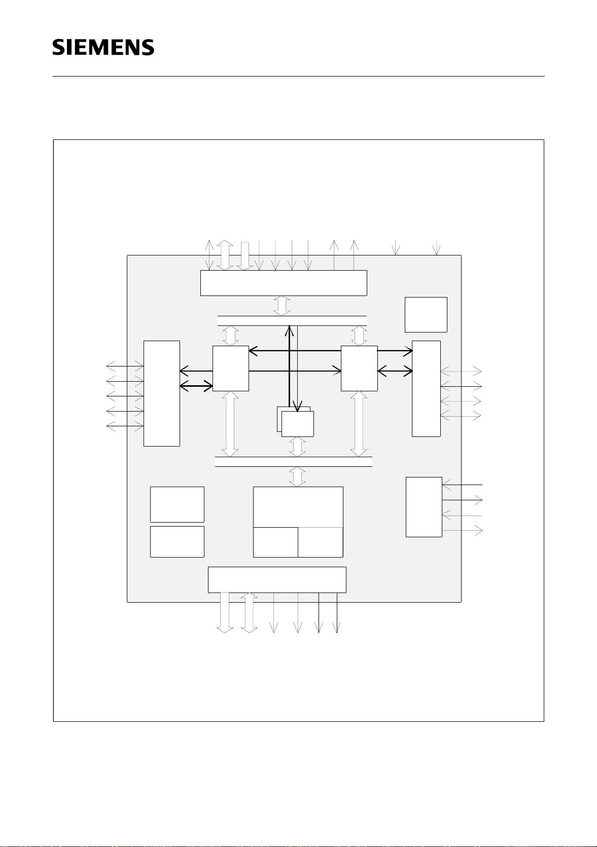
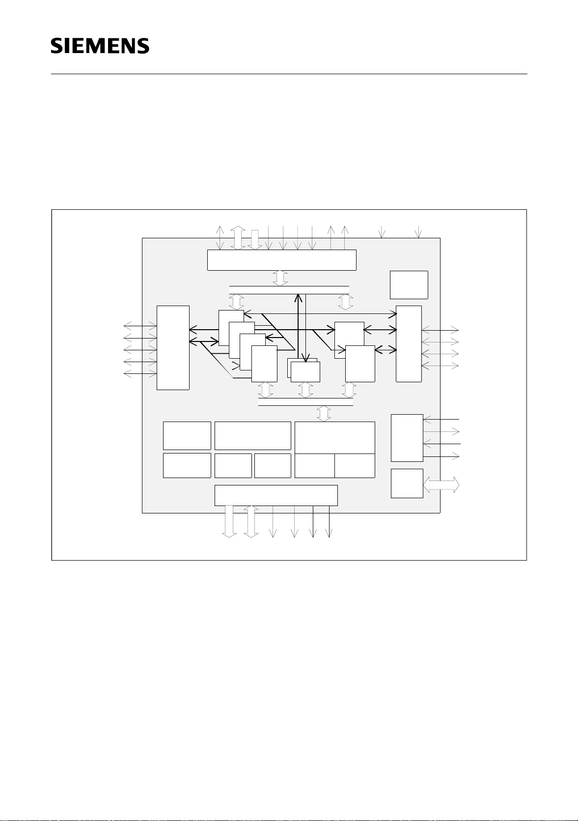
2 General Architecture and Functions
2.1 Architecture
Figure 6 shows a sketch of the PSB 7280 architecture with its most important functional
modules.
ALE
INTR#
SCLK
SR
ST
RFS
TFS
Ser ial
Audio
I/F
SIO
Audio
AD(0:7) WR#RD#
A(0:3)
Parallel Host Interface
Rec 1
Trm 1
Rec 2
Trm 2
Mailbox
256 byte
CS#
Mailbox
256 byte
IN T#
HDLC 1
HDLC 2
Re s e t
EA#
Mon, C/I
Contr ol
IOM/
PCM
DD
DU
DCL
FSC
CM1
CLKO
XTA L1
XTA L2
GP(0:3)
Config /Control
Register s
Timers
32 KW prog ram
ROM
8 KW dat a
X-ROM
2 K W d at a
X-RA M
1 KW data
X-RAM
DSP
Core
1 KW da ta
Y-RAM
BRG
clock
gen/
PLL
GPIO
I/F
External Memory Interface
CDS#
CA(0 : 15 ) C D(0 :15) CWR#C RD#
CPS#
Figure 6
The audio processing of the PSB 7280 is based on a 16-bit fixed point DSP core, SPCF
(Signal Processor Core Fast).
The Clock Generator is respons ible for generating the inte rnal clocks for the SPCF. A
Baud Rate Generator provides an output clock of programmable rate.
The Parallel Host Interface is used to control the circuit through an associated host via
interrupt handshake procedures. Alternatively, the circuit can be controlled via the serial
audio interface, thus enabling standalone applications to be implemented.
Communication between the host, if used, and the DSP is interrupt supported, via a fullduplex 256-byte on-chip Communication Memory Mailbox.
Semiconductor Group 21 Data Sheet 1998-07-01

PSB 7280
Two receive and two transmit audio channels are provided. They are input/output on the
ISDN Oriented Modular (IOM-2) or the Serial Audio Interface (SAI) interfaces in
individually programmable time-slots. These channels are accessed from the DSP
and/or the parallel host interface.
The two HDLC Controller ch annels can be serviced by the DSP or the parallel host
interface. The serial data for the HDLC controllers are located in programmable
time-slots on IOM-2 and/or SAI.
For development purposes, the External Memory Interface allows programs to be
executed from an external memory and external data memory to be used.
2.2 Functions
2.2.1 Summary of the Functions
The main functions implemented by the PSB 7238 are:
– G.728 compression/decompression (16 kbit/s)
– G.722 compression/decompression for 7-kHz audio (64, 56, 48 kbit/s)
– G.711 compression/decompression (64 kbit/s)
– Digit al sampling rate conversion (16 kHz - 8 Hz) for G.722 audio with 8-kHz code c
(bandwidth reduced to 3.4 kHz)
– Accepts/outputs uncompressed audio 8-bit PCM A/µ law or 16-bit linear format
– Uncompressed/compressed audio switchable between different interface
combinations (IOM/Serial Audio Interface, IOM/Host, Host/Host)
– Inband controlled H.221/H.223 oriented audio protocol, e.g. for direct serial
connection to videocodec (VCP of 8 × 8 Inc., formerly IIT Inc.)
– Outband controlled audio protocol with optimized data rate
– Stable reaction on interrupt handshake timing violations of e.g. a slow host
®
(Windows
PC)
For more details on the hardware (n ecess ary for a better und erstandi ng of som e of the
topics described in the pres ent chapter), plea se refer to the ot her chapters of thi s data
sheet.
Semiconductor Group 22 Data Sheet 1998-07-01

PSB 7280
2.2.2 Audio Functions and Supplementary Features
General
The uncompressed/compressed audio is applied to the interfaces as follows:
Uncompressed Audio Compressed Audio
IOM-2 (transparent) SAI (H.221/223 oriented audio protocol or
transparent)
IOM-2 (transparent) Host IF (interrupt handshake protocol with
minimized interrupt load for the host)
Host IF (interrupt handshake protocol) Host IF (interrupt handshake protocol)
“Transparent” means that data is received/transmitted in a time-slot without protocol.
1. Full Duplex G.728 Encoding/Decoding of One Audio Channel
Audio coding accordin g to ITU-T G.728 fixed point recomme ndation using Low Delay
Code Excited Prediction (LD-CELP, 16 kbit/s), offering toll quality audio. The postfilter of
the G.728 may be switched on (offe ring a higher quality impression) or off (providing
objective better S/N values).
2. Full Duplex G.722 Encoding/Decoding of One Audio Channel
Audio coding for 7-kHz voice using the Sub-Band Coded Adaptive Differential PCM
(SB-ADPCM) algorithm according to the G.722 Recommendation.
3. Serial H.221/223 Oriented Audio Protocol
The PSB 7280 supports a serial H.221/223 oriented audio protocol for direct connection
to a Videocodec (VCP of 8 × 8 Inc.). This protocol provides an outband synchronization
of the audio bit streams by using block structures for the compressed audio data.
Semiconductor Group 23 Data Sheet 1998-07-01
PSB 7280
3 Interfaces and Memory Organization
3.1 Interfaces
®
3.1.1 IOM
Electrical Interface
The IOM-2 interface is a 4-wire interface with two data lines (DD and DU, programmable
open drain or push-pul l), a data clock line (DCL inp ut/output) and a frame sync s ignal
(FSC input/output). The data clock is by def ault equal to twice the data rate (“Double
Rate”). However, DCL may be set equal to the data rate (“Single Rate”) by programming.
In standalone configuration the clock signal is always “Double Rate”.
In terminal applications , the bit rate on the interface is norm ally 768 kbit/s, in line card
applications it is 2048 kbit/s (for details, see IOM-2 Interface Reference Guide).
However, the data rate may be dif ferent (between 16 kbit/s a nd 4.096 Mbit/s and th e
DCL rate correspondin gly between 16 kHz and 4.096 MHz), since the interface ca n be
considered as a general purpose TDM (Time-Division Multiplex) highway.
-2 Interface
The total number of time-slots on the interface is not explicitly programmed: instead, the
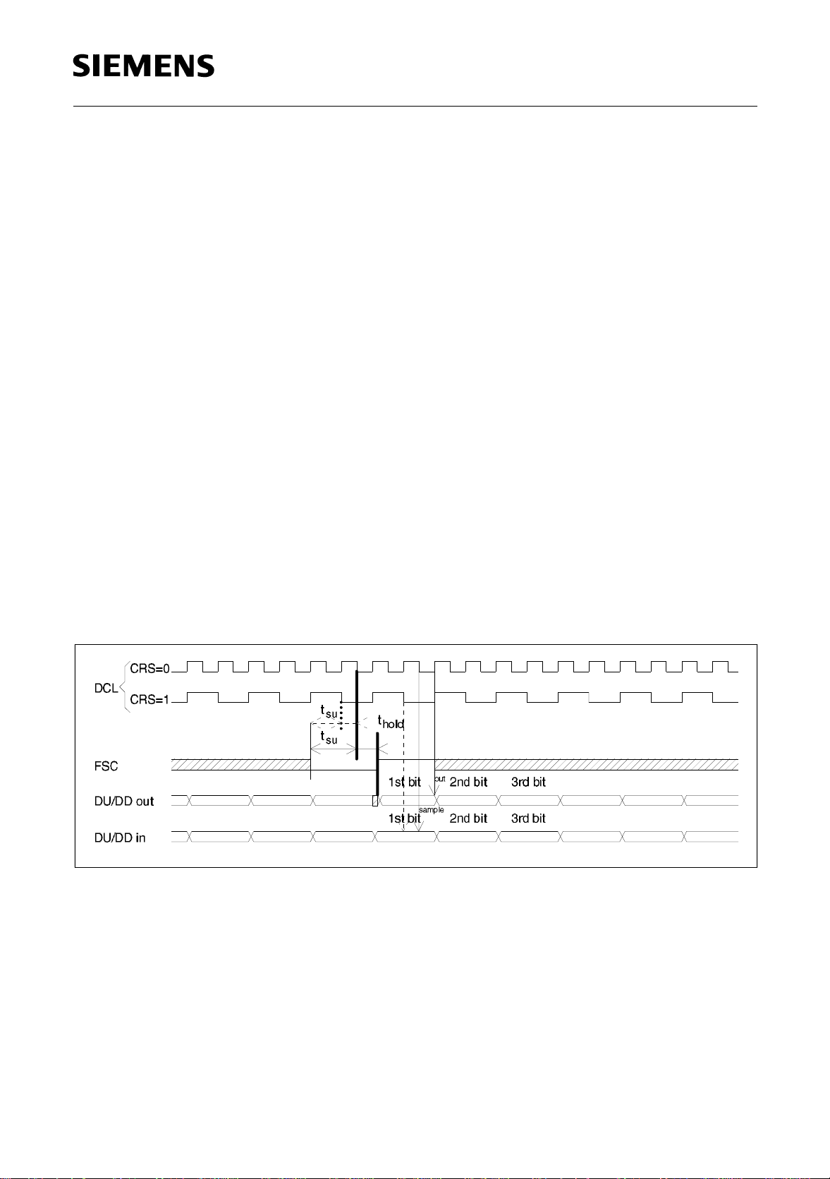
FSC signal (at repet ition rate 8 kHz) always marks the TDM physical frame b eginning
(see Figure 7).
Figure 7
DCL Bits on DU/DD are clocked out with the rising edge of DCL and
latched in with the falling edge of DCL. Frequency 16 kHz to
4.096 MHz.
FSC (8 kHz) Marks the beginning of the physical frame on DU and DD. The first
bit in the frame is output after the rising edge of FSC. The first bit in
the frame is latched in with the first falling edge after FSC has gone
“high” if CRS = 1, or after the second edge (at 3/4) if CRS = 0.
Semiconductor Group 24 Data Sheet 1998-07-01

PSB 7280
Channels
The following channe ls may be prog rammed on th e IOM-2 interfac e: two receive audio
channels, two transmit audio channels, one monitor channel, two C/I channels, two
receive and two transmit HDLC channels:
Audio receive 1 and receive 2 channels
Audio transmit 1 and transmit 2 channels
Independently programmable on DD or
DU, with programmable locations (start
at bit 1…512) and lengths (1…32 bits)
w.r.t. FSC
Monitor channel Programmable on DD(in)/DU(out) or
DD(out)/DU(in), with programmable
time-slot (3rd byte in multiplex 0, …, 15)
after FSC
Two C/I channels Programmable on DD(in)/DU(out) or
DD(out)/DU(in), with programmable
th
length (4 or 6 bits) and position (4
byte
in multiplex 0, …, 15) after FSC
Two HDLC receive and transmit channels Independently programmable on DD or
DU, with programmable locations (start
at bit 1…512) and lengths (1…256 bits)
w.r.t. FSC
The transfer of voice samples is performed with the help of an interrupt with repetit ion
rate 8 kHz derived from the FSC signal. A double- buff ered re gis ter i s p rovi ded for ea ch
channel, accessible from the DSP and from the parallel host interface. The double
buffered register ensures th at enough time is always provided for reading and writing
data before an overflow/underflow occurs, independent of the location of the time-slots.
Alternatively, the audio samples can be transferred between the DSP or Host and IOM-2
by using an interrupt generated when a programmable number (1…32) of bits are shifted
out (number independent of the time-slot length on the line).
Outside the time-slots whe re transmis sion ta kes pla ce the D U and DD lin es a re in high
impedance.
Semiconductor Group 25 Data Sheet 1998-07-01
PSB 7280
3.1.2 Serial Audio Interface
The Serial Audio Interface is a generic 5-line serial interface with the following lines:
SCLK Serial Bit Clock Input or output.
SR Serial Receive Input/output.
ST Serial Transmit Input/output.
RFS Receive Frame Sync Input or output.
TFS Transmit Frame Sync Input or output.
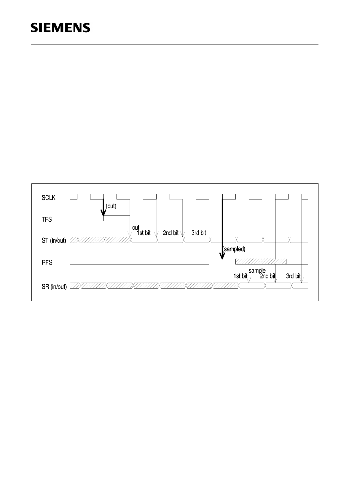
Figure 8 shows an example where RFS is input and TFS is output.
Figure 8
SCLK Input or output
Bits on SR/ST are clocked out with the rising edge of SCLK and latched in with
the falling edge of SCLK. Alternatively, bits can be clocked out with the falling
edge of SCLK and latched in with the rising edge. When SCLK is programmed
as output, it is derived from a programmable baud rate generator. Additionaly,
SLCK can be set to strobed operation.
Semiconductor Group 26 Data Sheet 1998-07-01

RFS Input or output
Marks the beginning of the physical frame on SR.
When input Sampled with a falling edge of SCLK.
When output Clocked out with the rising or falling edge of SCLK
TFS Input or output
Marks the beginning of the physical frame on ST.
When input Sampled with a falling edge of SCLK .
When output Clocked out with the rising or falling edge of SCLK
PSB 7280
(duration = 1 SCLK period).
Repetition rate (continuous mode) or number of
pulses (burst mode) is programmable
(duration = 1 SCLK period).
Repetition rate (continuous mode) or number of
pulses (burst mode) is programmable.
SCLK is derived from the chip-internal DSP clock via a programmable baud rate
generator (division factor 1, 2, 3, …, 1024).
The Receive Frame Sync (RFS), when programmed as output, has two selectable
modes of operation:
–In the continuous mode (CONT = 1), pulses are continuously generated, separated
by a distance
16 × (PRD + 1) bits from each other, where PRD = 0, …, 255.
–In the burst mode (CONT = 0), pulses are generated upon command a
programmable number of times (REP + 1: 1, …, 1024), spaced 16 bits apart from
each other.
The same applies to TFS when it is an output.
Semiconductor Group 27 Data Sheet 1998-07-01

PSB 7280
Channels
Two Audio receive and transmit channels Independently programmable on SR, ST,
DU or DD with programmable locations
(start at bit 1…512) and lengths
(1…32 bits) with respect to RFS/TFS.
Two HDLC receive and transmit channels Independently programmable on SR, ST,
DU or DD with programmable locations
(start at bit 1…512) and lengths
(1…256 bits) with respect to RFS/TFS.
3.1.3 Parallel Host Interface
The parallel host interface can be selected to be either of the
(1) Motorola type with control signals CS
,R/W, DS
(2) Siemens/Intel demultiplexed bus type with control signals CS, WR, RD
(3) or of the Siemens/Intel multiplex ed address/data bus type with control signals CS,
, RD, ALE
WR
The selection is performed via pin ALE as follows:
V
V
→ (1)
DD
→ (2)
SS
ALE tied to
ALE tied to
Edge on ALE → (3)
The occurence of an edge on ALE, either positive or negative, at any time durin g the
operation immediately se lects the multiplexed bus type. A return to one of the other is
possible only if a hardware reset is issued.
3.1.4 External Memory Interface
The external memory interface allows the connection of both program and data
memories to the PSB 7280. The access to either type of memory is determine d by the
signals CPS
interface used as a program memory interface is normally not needed, but is reserved
for development purposes.
and CDS, respectively. In standard applications, the external memory
The upper 32k half (800 0
-FFFFH) of the address spac e is reserved for execution of
H
software from external memory.
For executing software in the lower address range 0000
-7FFFH, a control line EA
H
(External Access) determines whether program is fetched from internal or external
memory. Thus, in standard applications, the EA
line should always be “high”.
The DSP program execution can be controlled from the outside by loading the
PC-counter of the DSP via the parallel host interface.
Semiconductor Group 28 Data Sheet 1998-07-01

PSB 7280
The external memory interface implements:
– protection against reading the internal ROM.
3.1.5 Clock Interface
The chip internal clock is derived from a crys tal connected across XTAL1,2 or from an
external clock input via pin XTAL1. Two different cloc k options are prov ided, control led
by the clock mode pin CM1.
These clock modes are:
CM1 = 0 The internal clock circuitry generates a frequency 4.5 times the input
on XTAL1(,2). The internal frequency required is 34.56 MHz and is
obtained by providing a frequency of 7.68 MHz on XTAL1 input.
CM1 = 1 The internal frequency is directly input via XTAL1(,2). When using a
crystal, a 34.56 MHz crystal swinging at its basic harmonic has to be
connected to XTAL1,2.
After reset the pin CLKO outputs a frequency of 7.68 MHz, independent of the selection
of CM1 bit. Alternatively, CLKO can be programmed to output the frequency of a
programmable divider (CKOS bit in register 2002
the internal clock divided by a prog rammable baud rate factor (1, 2, 3, …, 2
). Thus, a clock of frequency equal to
H
19
) can be
generated.
When using the PLL (CM1 = 0), it is made sure that during reset phase CLKO delivers a
continuous 7.68 MHz clock. When using the non -PLL mode (CM1 = 1) CLKO goes low
while reset phase.
3.2 Shared Memories
Note: The absolute addresses for the different internal register banks and memories are
given here and in the rest of this Data Sheet both as seen from the host and from
the embedded DSP, the latter information being included for the sake of
completeness only.
Directly Accessible Register Bank (DARB)
The host accesses directly via its 8-bit address bus the s o-called Directly Acces sible
Register Bank (DARB) located between DSP addresses 3000
and 30FFH.
H
Semiconductor Group 29 Data Sheet 1998-07-01
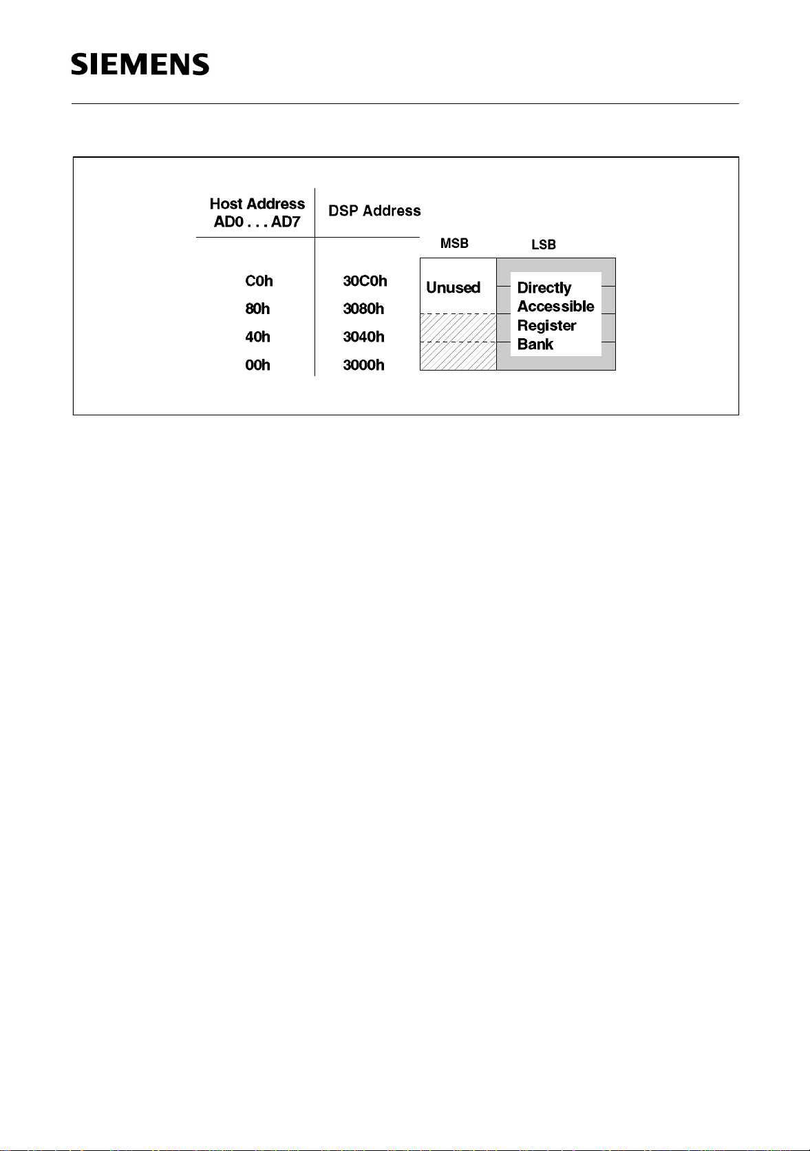
Figure 9
PSB 7280
This area is in turn divided into four blocks of 64 bytes each according to their functions.
Not all the addresses in each of these 64-byte areas are used. An overview of the
functions of these 64-byte areas is given in Figure 10, please refer also to the
appropriate chapters for a detailed description.
1. Locations for reading and writing samples “in real ti me” from/to the seria l interfaces
(IOM-2 and serial audio interface) - Input/Output area (see Chapter 3.3.1).
2. Area for communication between the host and the embe dded DSP, fo r program ming
parameters and reporting status conditions - DSP/Host Com area (see Chapter 3.3.2
and Chapter 3.3.3).
3. Register bank for HDLC Controller 1 - accessed by host if HHA1 (configuration bit) is
‘1’ - HDLC1.
4. Register bank for HDLC Controller 2 - accessed by host if HHA2 (configuration bit) is
‘1’ - HDLC2.
Semiconductor Group 30 Data Sheet 1998-07-01
 Loading...