


Siemens PSB7230 Datasheet

ICs for Communications
Joint Audio Decoder-Encoder for Analog Videophone
JADE AN
PSB 7230 Version 2.1
Data Sheet 1998-07-01
DS 1

PSB7230
Revision History: Current Version: 1998-07-01
Previous Version: Prelimiinary Data Sheet 02.97 (V 1.2)
Page
(in previous
Version)
Page
(in current
Version)
Subjects (major changes since last revision)
For questions on technology, delivery and prices please contact the Semiconductor Group Offices
in Germany or the Siemens Companies and Representatives worldwide: see our webpage at
http://www.siemens.de/semiconductor/communication
IOM®, IOM®-1, IOM®-2, SICOFI®, SICOFI®-2, SICOFI®-4, SICOFI®-4µC, SLICOFI®, ARCOFI
ARCOFI
SICAT
MUSAC
®
-SP, EPIC®-1, EPIC®-S, ELIC®, IPAT®-2, ITAC®, ISAC®-S, ISAC®-S TE, ISAC®-P, ISAC®-P TE, IDEC®,
®
, OCTAT®-P, QUAT®-S are registered trademarks of SiemensAG.
™
-A, FALC™54, IWE™, SARE™, UTPT™, ASM™, ASP™, DigiTape™ are trademarks of SiemensAG.
®
, ARCOFI®-BA,
Edition 1998-07-01
Published by Siemens AG,
HL SP,
Balanstraße 73,
81541 München
© Siemens AG 1998.
All Rights Reserved.
Attention please!
As far as patents or other rights of third parties are concerned, liability is only as sumed for components, not for
applications, processes and circuits implemented within components or as s emblies.
The information describes the type of component and shall not be considered as assured characteristics.
Terms of delivery and rights to change design reserved.
Due to technical requirements components may contain dangerous substances. For inf orm ation on the t y pes in
question please contact your nearest Siemens Office, Semic onductor Group.
Siemens AG is an approved CECC manufacturer.
Packing
Please use the recycling operators known to y ou. W e can also help you – get in t ouc h w it h your nearest s ales
office. By agreement we will take packing material back, if it is sorted. You must bear the costs of transport.
For packing material that is returned to us unsorted or which we are not obliged to accept, we shall have to invoice
you for any costs incurred.
Components used in life-support devices or systems must be expressly authorized for such purpose!
Critical components
systems
1A critical component is a component used in a life-support device or system whose failure can reasonably be
2Life support devices or systems are intended (a) to be implanted in the human body, or (b) to support and/or
2
with the express written approval of the Semiconductor Group of Siemens AG.
expected to cause the failure of that life-support device or system, or to affect its safety or effectiveness of that
device or system.
maintain and sustain human life. If they fail, it is reasonable to as sum e that t he health of the user may be endangered.
1
of the Semiconductor Group of Siemens AG, may only be used in life-support devices or

PSB 7230
Table of Contents Page
1 Introduction . . . . . . . . . . . . . . . . . . . . . . . . . . . . . . . . . . . . . . . . . . . . . . . . .5
1.1 Feature List . . . . . . . . . . . . . . . . . . . . . . . . . . . . . . . . . . . . . . . . . . . . . . . . . .5
1.2 Overview . . . . . . . . . . . . . . . . . . . . . . . . . . . . . . . . . . . . . . . . . . . . . . . . . . . .6
1.3 Logic Symbol . . . . . . . . . . . . . . . . . . . . . . . . . . . . . . . . . . . . . . . . . . . . . . . . .8
1.4 Pin Configuration . . . . . . . . . . . . . . . . . . . . . . . . . . . . . . . . . . . . . . . . . . . . . .9
1.5 Pin Description . . . . . . . . . . . . . . . . . . . . . . . . . . . . . . . . . . . . . . . . . . . . . . .10
1.6 System Integration . . . . . . . . . . . . . . . . . . . . . . . . . . . . . . . . . . . . . . . . . . . .16
1.6.1 H.324 Desktop Videoconferencing Solution for POTS . . . . . . . . . . . . . .17
1.6.2 Low Cost H.324 Desktop Videoconferencing with Software Video . . . . .19
1.6.3 LAN Videoconferencing . . . . . . . . . . . . . . . . . . . . . . . . . . . . . . . . . . . . . .20
1.6.4 Standalone H.324/H.323 Videophone . . . . . . . . . . . . . . . . . . . . . . . . . . .21
1.6.5 Internet Telephone Access in Line Card . . . . . . . . . . . . . . . . . . . . . . . . .22
2 General Architecture and Functions . . . . . . . . . . . . . . . . . . . . . . . . . . . .24
2.1 Architecture . . . . . . . . . . . . . . . . . . . . . . . . . . . . . . . . . . . . . . . . . . . . . . . . .24
2.2 Functions . . . . . . . . . . . . . . . . . . . . . . . . . . . . . . . . . . . . . . . . . . . . . . . . . . .26
2.3 Summary of the Functions . . . . . . . . . . . . . . . . . . . . . . . . . . . . . . . . . . . . . .26
2.3.1 Audio Functions and Supplementary Features . . . . . . . . . . . . . . . . . . . .26
3 Interfaces and Memory Organization . . . . . . . . . . . . . . . . . . . . . . . . . . . .28
3.1 Interfaces . . . . . . . . . . . . . . . . . . . . . . . . . . . . . . . . . . . . . . . . . . . . . . . . . . .28
3.1.1 IOM-2 Interface . . . . . . . . . . . . . . . . . . . . . . . . . . . . . . . . . . . . . . . . . . . .28
3.1.2 Serial Audio Interface . . . . . . . . . . . . . . . . . . . . . . . . . . . . . . . . . . . . . . .30
3.1.3 Parallel Host Interface . . . . . . . . . . . . . . . . . . . . . . . . . . . . . . . . . . . . . . .32
3.1.4 External Memory Interface . . . . . . . . . . . . . . . . . . . . . . . . . . . . . . . . . . . .32
3.1.5 Clock Interface . . . . . . . . . . . . . . . . . . . . . . . . . . . . . . . . . . . . . . . . . . . . .33
3.2 Shared Memories . . . . . . . . . . . . . . . . . . . . . . . . . . . . . . . . . . . . . . . . . . . .34
3.3 Directly Accessible Register Bank . . . . . . . . . . . . . . . . . . . . . . . . . . . . . . . .36
3.3.1 Input/Output Registers . . . . . . . . . . . . . . . . . . . . . . . . . . . . . . . . . . . . . . .36
3.3.2 DSP/Host Com Area . . . . . . . . . . . . . . . . . . . . . . . . . . . . . . . . . . . . . . . .39
3.3.2.1 Access to DSP/Host Com Area . . . . . . . . . . . . . . . . . . . . . . . . . . . . . .39
3.4 Mailbox . . . . . . . . . . . . . . . . . . . . . . . . . . . . . . . . . . . . . . . . . . . . . . . . . . . .44
3.4.1 DSP/Host Com Area with a Demultiplexed Host Interface . . . . . . . . . . .46
4 Functional Blocks . . . . . . . . . . . . . . . . . . . . . . . . . . . . . . . . . . . . . . . . . . .49
4.1 Oscillator and Baud Rate Generator . . . . . . . . . . . . . . . . . . . . . . . . . . . . . .49
4.2 Audio and Data Reception/Transmission . . . . . . . . . . . . . . . . . . . . . . . . . .52
4.3 Serial Data Controller . . . . . . . . . . . . . . . . . . . . . . . . . . . . . . . . . . . . . . . . .64
4.4 IOM-2 Functions . . . . . . . . . . . . . . . . . . . . . . . . . . . . . . . . . . . . . . . . . . . . .67
4.4.1 Monitor Channel Protocol . . . . . . . . . . . . . . . . . . . . . . . . . . . . . . . . . . . .68
4.4.2 C/I Channel . . . . . . . . . . . . . . . . . . . . . . . . . . . . . . . . . . . . . . . . . . . . . . .74
4.5 Programming Indirectly Accessible Registers . . . . . . . . . . . . . . . . . . . . . . .77
4.5.1 Programming via Parallel Host Interface . . . . . . . . . . . . . . . . . . . . . . . . .77
Semiconductor Group 3 Data Sheet 1998-07-01

PSB 7230
Table of Contents Page
5 Register Description . . . . . . . . . . . . . . . . . . . . . . . . . . . . . . . . . . . . . . . . .78
5.1 Interrupt Structure . . . . . . . . . . . . . . . . . . . . . . . . . . . . . . . . . . . . . . . . . . . .78
5.2 Interrupt Status Registers . . . . . . . . . . . . . . . . . . . . . . . . . . . . . . . . . . . . . .79
5.3 Indirectly Accessible Configuration and Control Registers . . . . . . . . . . . . .82
5.4 Serial Data Controller Registers . . . . . . . . . . . . . . . . . . . . . . . . . . . . . . . .101
6 Firmware Features . . . . . . . . . . . . . . . . . . . . . . . . . . . . . . . . . . . . . . . . . .113
6.1 Basic Functions . . . . . . . . . . . . . . . . . . . . . . . . . . . . . . . . . . . . . . . . . . . . .114
6.1.1 Firmware Version Number . . . . . . . . . . . . . . . . . . . . . . . . . . . . . . . . . . .114
6.1.2 Software Reset . . . . . . . . . . . . . . . . . . . . . . . . . . . . . . . . . . . . . . . . . . .115
6.1.3 Power Down Command . . . . . . . . . . . . . . . . . . . . . . . . . . . . . . . . . . . . .116
6.2 Audio Interfaces . . . . . . . . . . . . . . . . . . . . . . . . . . . . . . . . . . . . . . . . . . . . .117
6.2.1 Compressed Audio Protocols and Control of JADE AN . . . . . . . . . . . .119
6.2.1.1 Outband Control of JADE AN . . . . . . . . . . . . . . . . . . . . . . . . . . . . . .119
6.2.1.2 Compressed Audio Protocol with Outband Control . . . . . . . . . . . . . .130
6.2.1.3 Compressed Audio Protocol with Inband Control . . . . . . . . . . . . . . .132
6.2.1.4 Control Pipeline . . . . . . . . . . . . . . . . . . . . . . . . . . . . . . . . . . . . . . . . .138
6.2.2 Uncompressed Data Protocol . . . . . . . . . . . . . . . . . . . . . . . . . . . . . . . .144
6.2.3 Audio Interface Timings . . . . . . . . . . . . . . . . . . . . . . . . . . . . . . . . . . . . .145
6.2.3.1 Uncompressed Data: Host IF, Compressed Data: Host IF . . . . . . . .145
6.2.3.2 Uncompressed Data: IOM IF, Compressed Data: Host IF . . . . . . . .153
6.2.3.3 Uncompressed Data: IOM IF, Compressed Data: Serial Audio Interface
(SAI) 162
7 Electrical Specification . . . . . . . . . . . . . . . . . . . . . . . . . . . . . . . . . . . . . .165
7.1 Absolute Maximum Ratings . . . . . . . . . . . . . . . . . . . . . . . . . . . . . . . . . . . .165
7.2 Operating Conditions . . . . . . . . . . . . . . . . . . . . . . . . . . . . . . . . . . . . . . . . .165
7.3 DC Characteristics . . . . . . . . . . . . . . . . . . . . . . . . . . . . . . . . . . . . . . . . . . .165
7.4 Capacitances . . . . . . . . . . . . . . . . . . . . . . . . . . . . . . . . . . . . . . . . . . . . . . .167
7.5 Oscillator Circuit . . . . . . . . . . . . . . . . . . . . . . . . . . . . . . . . . . . . . . . . . . . . .167
7.6 XTAL 1,2 Recommended Typical Crystal Parameters . . . . . . . . . . . . . . .167
7.7 AC Characteristics . . . . . . . . . . . . . . . . . . . . . . . . . . . . . . . . . . . . . . . . . . .168
7.7.1 Testing Waveform . . . . . . . . . . . . . . . . . . . . . . . . . . . . . . . . . . . . . . . . .168
7.7.2 Parallel Host Interface Timing . . . . . . . . . . . . . . . . . . . . . . . . . . . . . . . .168
7.7.3 IOM-2 Interface Timing . . . . . . . . . . . . . . . . . . . . . . . . . . . . . . . . . . . . .172
7.7.4 Serial Audio Interface Timing . . . . . . . . . . . . . . . . . . . . . . . . . . . . . . . . .176
7.7.5 External Memory Interface . . . . . . . . . . . . . . . . . . . . . . . . . . . . . . . . . . .178
8 Package Outlines . . . . . . . . . . . . . . . . . . . . . . . . . . . . . . . . . . . . . . . . . . .179
Semiconductor Group 4 Data Sheet 1998-07-01
Joint Audio Decoder-Encoder for Analog Videophone
PSB 7230
JADE AN
Version 2.1
1 Introduction
1.1 Feature List
Functions
– G.723 V5.1 Compression/Decompression (6.3,
5.3 Kbit/s)
– Accepts/outputs uncompressed audio in 8-bit PCM
A/µ law or 16-bit linear format
– G.711 Compression/Decompression (64 Kbit/s)
– Uncompressed/compressed audio switchable between different interface
®
combinations (IOM
/Serial Audio Interface, IOM/Host, Host/Host)
– Inband controlled H.221/H.223 oriented audio protocol, e.g. for direct serial
connection to Videocodec (VCP of 8 × 8 Inc., formerly IIT Inc.) as well as host based
solutions
– Outband controlled audio protocol with optimized data rate
– Stable reaction on interrupt handshake timing violations of e.g. a slow host
®
(Windows
PC)
P-TQFP-100
System On-Chip Functions
– One universal serial transparent data controller
– IOM-2 Monitor and C/I channels
– Generation of programmable system clock output
Interfaces
– 4-line IOM-2/PCM interface (programmable master or slave)
– 5-line serial audio interface, e.g. for connection to Videocodec/H.221/223 processor
– Parallel 8-bit Host interface
– 4-line general purpose interface
Type Ordering Code Package
PSB 7230 Q67101-H6864 P-TQFP-100
Semiconductor Group 5 Data Sheet 1998-07-01

PSB 7230
Introduction
Control
– Programmable via Parallel Host Interface
– Operating parameters and mode settings via a register bank
– Access to audio channels and serial transparent data controller from DSP or an
external Host
– Interface to external software via a full-duplex 256-byte on-chip mailbox
– H.221/H.223 oriented inband configuration/mode switching
General
– Supply voltage: 3.0 - 3.6 V
– Additional 4.5 to 5.5 V supply for connection to 5 V systems without external
components
– Ambient temperature range 0 °C to + 70 °C
– P-TQFP-100 package
1.2 Overview
The PSB 7230 Joint Audio Decoder Encoder for Analog Videophones (JADE AN) is a
device which implements voice compression algorithms using the Algebraic Code
Excited Linear Prediction (ACELP) and the Multi-Pulse Maximum Likelihood
Quantization (MP-MLQ ) standard as defined in t he ITU-T G.723 Recommendatio n. In
addition G.711 PCM audio coding is also supported.
Thus, in G.723 mode it compresses the PCM (8 bit A-/µ-law) or 16 bit linea r voic e sign al
into 5.3 Kbit/s (ACELP) or 6.3 Kbit/s (MP-MLQ) bit stream, and vice versa. The
implementation com plies with the newest ITU-T C-c ode V5.1 and includes the G.72 3
Annex A (Voice Activity Detection and Comfort Noise Generation).
The JADE AN finds applications in
– Analog Videophones (H.324)
– Networks (e.g. LANs) for packetized voice (H.323)
– Video Conference Systems
– Corporate Network voice concentrators, multiplexers and gateways
– Data-over-voice and Voice-over-data terminals.
Other potential application areas are:
– Networks (e.g. LANs) for packetized voice
– Digital Added Main-Line (DAML) & Digital Circuit Multiplication Equipment (DCME)
– Voice storage e.g. in PC based applications
– Message recording and distribution.
The interfaces of the JADE allow a seamless integration into IOM-2 based systems. After
the circuit is set up in the proper mode of operation and parameter settings are
programmed by a controlling so ftware, the circuit runs independen tly of the rest of the
Semiconductor Group 6 Data Sheet 1998-07-01

PSB 7230
Introduction
system. Status and control information to/from the JADE can be transferred either
inband the compressed audio data via the corresp onding sel ect ed interf ace or outband
using an 8-bit parallel host interface.
The audio frontend data can be exchanged either through the host interface or the IOM-2
interface. In the latter case the Siemens ARCOFI SP can be connected providing
half-duplex hands free or a Siem ens AC E (ac ous tic echo canceller circuit) together w ith
an ARCOFI BA providing full duplex handsfree.
The default configuration of the JADE is such, that in a videoconferencing system using
the 8x8 (formerly IIT) VCP (Video Codec and Multimedia Communications Pro cessor)
the Siemens PSB 7230 can work standalon e without the nee d of external initi alization.
I.e., no host is needed in this c ase and the full communicati on is automatical ly started
between the VCP and the Siemens PSB 7230.
The voice compression algorith ms are implem ented by an embedd ed 16-bit fixed point
Digital Signal Processor with all memories internal and no external memory needed.
Integration of these and other features, as well as perfectly matched interfaces with other
ICs allows for the implementation of highly optimized, low cost system solutions e.g. for
Videophones, Data-over-voice and Channel Multiplexing equipment.
For system integration, a serial data channel is impleme nted which can be servi ced by
an attached host (or the on -chip DSP). Syst em functions an d communication be tween
the chip and an external controller is supported by a full-duplex 256-byte on-chip mailbox
communication memory.
The circuit is offered in a Quad Flat Pack package with 100 pins (P-TQFP-100: size
14 × 14 mm, pitch 0.5 mm, height 1.4 mm).
Note: This Data Sheet giv es a thoro ugh descrip tion of the functi ons and h ardware that
forms the base of PSB 7230. It includes information that is not needed for the
PSB 7230 as a ‘ready to use plug and play' G.723/G.711 audio compression
device.
Semiconductor Group 7 Data Sheet 1998-07-01
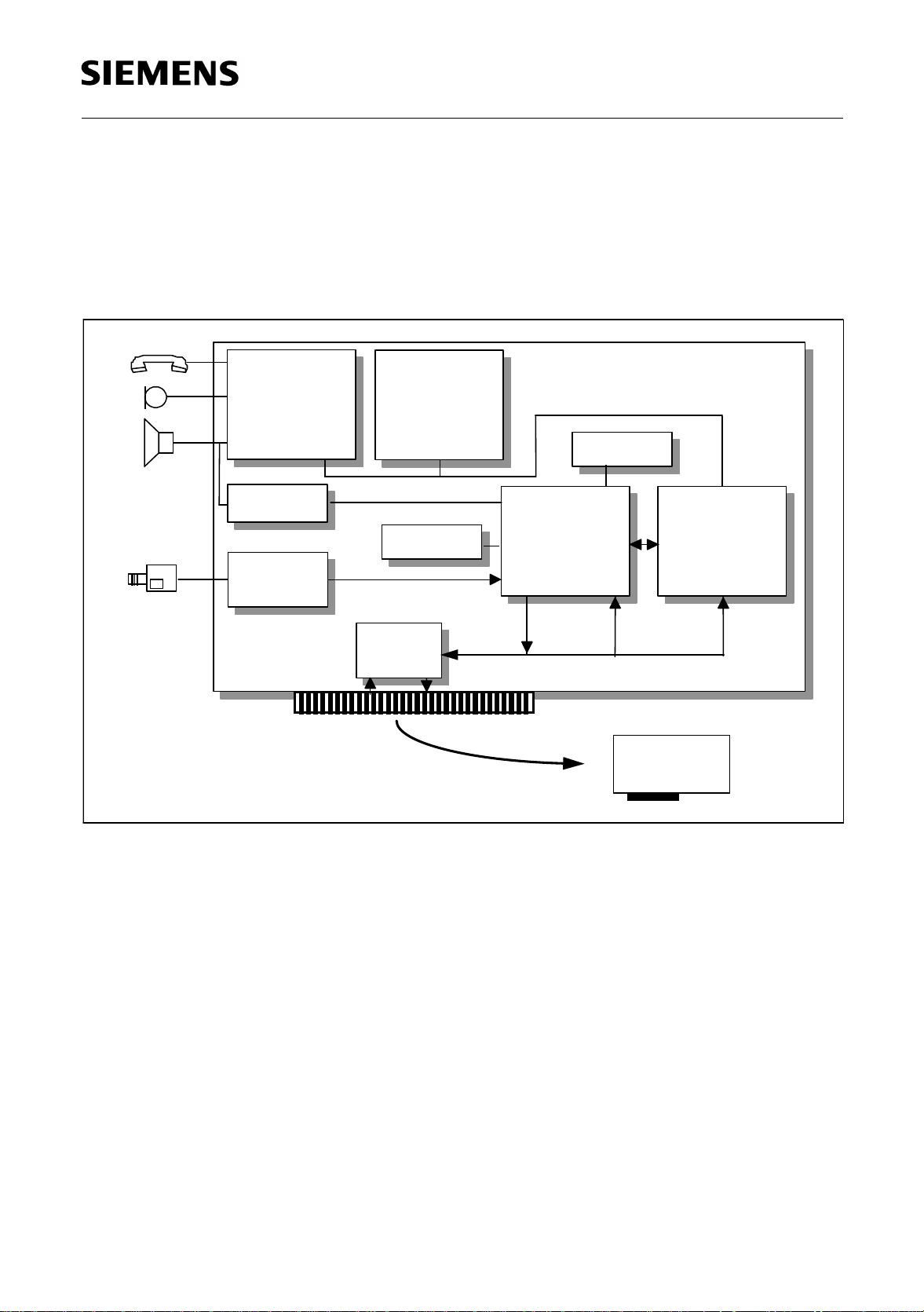
1.3 Logic Symbol
Parallel Host Interface
RD#
A(0:3)
WR#
(R/W#)
(DS#)
CS#
ALE
PSB 7230
Introduction
INT#AD(0:7)
RESET
EA #INTR#
Serial
Audio
Interface
Power
Su ppl y
SIO
SCLK
SR
ST
RFS
TFS
VDD
VDDAP, VDDP
VS S
VDDA
VSSA, VSSAP
CA(0: 15) CD(0:15)
PSB 7230
CRD#
CWR#
CPS#
CDS#
GPIO(0:3)
DD
DU
DCL
FSC
CM1
XTAL1
XTAL2
CLKO
IOM -2
Interface
System
Clock
Interface
Exter n al Memory Interface
GP IO Inter fa ce
Figure 1
Semiconductor Group 8 Data Sheet 1998-07-01
1.4 Pin Configuration
SRSTRFS
TFSA3CM1
PSB 7230
Introduction
VSS
VDD
VSSA
XTAL2
XTAL1
VDDA
VSSAP
VDDAP
CLKO
SIO
RESETA1A0
GP3
GP2
GP1
GP0
VSS
CD0
SCLK
ALE
CS#
RD#
WR#
AD7
AD6
AD5
AD4
VDDP
VSS
VDD
AD3
AD2
AD1
AD0
INTR#
INT#
A2
FSC
DCL
DU
DD
CA1 5
CD15
1
76
PSB 7230
P-TQFP-100
CRD#
51
CA9
CD9
CA8
26
CA14
CD1 4
VDDP
VSS
CA13
CD1 3
CA12
CD1 2
VDD
VSS
VDD
CA11
CD1 1
CA10
CD1 0
VDD
VSS
EA#
CDS #
CPS#
CWR#
CA0
CD1
CA1
VSS
VDDP
CD2
CA2
CD3
CA3
VSS
VDD
CD4
CA4
CD5
CA5
VDD
VSS
VDD
CD6
CA6
CD7
CA7
VSS
VDD
CD8
Figure 2
Semiconductor Group 9 Data Sheet 1998-07-01
PSB 7230
Introduction
1.5 Pin Description
Table 1 Parallel Host Interface
Pin No. Symbol Function Descriptions
16 AD0 I/O Multiplexed Bus Mode: Address/Data Bus. Transfers
15 AD1 I/O
14 AD2 I/O
13 AD3 I/O
9 AD4 I/O
8 AD5 I/O
7 AD6 I/O
6 AD7 I/O
addresses from the host to JADE and data between the
host and the JADE
Demultiplexed Bus Mode: Data bus. Transfers data
between the host and the JADE
4 DS I Data Strobe.
The rising edge marks the end of a valid read or write
operation (Motorola bus mode).
RD
5 R/W I Read/Write.
WR
3CS
2 ALE I Address Latch Enable.
I Read.
This signal indicates a read operation (Siemens/Intel
bus mode).
A 1 (“high“) identifies a valid host access as a read
operation. A 0 identifies a valid host access as a write
operation (Motorola bus mode)
I Write.
This signal indicates a write operation (Siemens/Intel
bus mode).
I Chip Select.
A “high” on this line indicates an address on AD(0:7)
(multipexed bus mode only). ALE also selects the
interface mode
82 A0 I Address Bits A(0:3) (demultiplexed bus type)
83 A1 I
19 A2 I
96 A3 I
Semiconductor Group 10 Data Sheet 1998-07-01
Table 1 Parallel Host Interface (cont’d)
Pin No. Symbol Function Descriptions
17 INTR O (OD) Interrupt Real-time.
Interrupt output line for high priority interrupt status
(serial audio receive/transmit, serial HDLC data
receive/transmit data) to host.
PSB 7230
Introduction
18 INT
O (OD) Interrupt Request.
Interrupt output line for all other interrupt states.
Table 2 IOM-2 Interface
Pin No. Symbol Function Descriptions
23 DD I/O(OD) Data Downstream on IOM-2/PCM interface.
22 DU I/O(OD) Data Upstream on IOM-2/PCM interface.
21 DCL I/O(OD) Data Clock.
Clock frequency is twice the data rate, or equal to the
data rate.
20 FSC I/O(OD) Frame Sync.
Marks the beginning of a physical IOM-2 or PCM frame.
Table 3 Serial Audio Interface
Pin No. Symbol Function Descriptions
1 SCLK I/O Serial Clock.
Serial clock for SR and ST.
100 SR I/O(OD) Serial Data Receive.
V
Should be connected to
via a pulldown resistor if not
SS
used.
99 ST I/O(OD) Serial Data Transmit.
98 RFS I/O Audio Receive Frame Sync.
97 TFS I/O Audio Trans mit Frame Sync .
Semiconductor Group 11 Data Sheet 1998-07-01
Table 4 System Clocks
Pin No. Symbol Function Descriptions
90 XTAL1 I Crystal In or Clock In.
If a crystal is used, it is connected between XTAL1 and
XTAL2. If a clock signal is provided (via an external
oscillator), this signal is input via XTAL1. In this case the
XTAL2 output is to be left non-connected. The XTAL1
input has to be 50% duty cycle and must not exceed the
voltage range between
91 XTAL2 O Crystal Out.
Left unconnected if a crystal is not used.
86 CLKO O Clock Out.
Output clock of frequency equal to the internal frequency
divided by a programmable factor.
V
SSA
and V
DDA
PSB 7230
Introduction
.
Table 5 External Memory Interface (for Development Purposes only)
Pin No. Symbol Function Descriptions
75 CA0 O C-Bus Address.
73 CA1 O Used for addressing ROM or RAM external to the chip.
69 CA2 O Is to be left NC if not used.
67 CA3 O
63 CA4 O
61 CA5 O
56 CA6 O
54 CA7 O
50 CA8 O
48 CA9 O
39 CA10 O
37 CA11 O
32 CA12 O
30 CA13 O
26 CA14 O
24 CA15 O
Semiconductor Group 12 Data Sheet 1998-07-01
PSB 7230
Introduction
Table 5 External Memory Interface (for Development Purposes only) (cont’d)
Pin No. Symbol Function Descriptions
76 CD0 I/O C-Bus Data.
74 CD1 I/O Data bus for external ROM or RAM. Is to be left NC if not
70 CD2 I/O
68 CD3 I/O
64 CD4 I/O
62 CD5 I/O
57 CD6 I/O
55 CD7 I/O
51 CD8 I/O
used.
49 CD9 I/O
40 CD10 I/O
38 CD11 I/O
33 CD12 I/O
31 CD13 I/O
27 CD14 I/O
25 CD15 I/O
43 EA
47 CRD
I External program Access enable
O C-Bus Read to external memories.
When “high”, an access to program address range
(0000
ROM. Access to 8000
- 7FFFH) fetches an instruction from on-chip
H
- FFFFH addresses external
H
memory via the External Memory Interface.
When “low”, an access to 0000
0000
- 7FFFH, normally reserved for on-chip software)
H
- FFFFH (including
H
accesses external program memory via the External
Memory Interface.
Left NC if not used.
46 CWR
O C-Bus Write to external memories.
Left NC if not used.
45 CPS
O C-Bus Select line for external program memory.
Left NC if not used.
44 CDS
O C-Bus Select line for external data memory.
Left NC if not used.
Semiconductor Group 13 Data Sheet 1998-07-01
Table 6 General Control
Pin No. Symbol Function Descriptions
95 CM1 I Clock Mode
Selects the option for the generation of the DSP internal
working clock.
85 SIO I/O Serial I/O line.
When programmed as input, a rising or falling
(selectable) edge on this line may generate a maskable
interrupt INT
(host) or INT1 (DSP).
When programmed as output, its state is directly
controlled by the DSP or the host.
84 RESET I Reset input. Reset time: > 1 ms.
PSB 7230
Introduction
Table 7 General Purpose I/O Interface
Pin No. Symbol Function Descriptions
81 GP0 I/O (OD) General purpose I/O pins
80 GP1 I/O(OD)
79 GP2 I/O(OD)
78 GP3 I/O(OD)
Table 8 Power Supply
Pin No. Symbol Function Descriptions
11
29
35
42
53
59
V
V
V
V
V
V
SS
SS
SS
SS
SS
SS
I Ground (common to VDD and V
I
I
I
I
I
DDP
) .
66
72
77
94
Semiconductor Group 14 Data Sheet 1998-07-01
V
V
V
V
SS
SS
SS
SS
I
I
I
I
Table 8 Power Supply (cont’d)
Pin No. Symbol Function Descriptions
PSB 7230
Introduction
12 V
36
60
93
34
41
52
58
65
10
28
71
89
92
V
V
V
V
V
V
V
V
V
V
V
V
V
DD
DD
DD
DD
DD
DD
DD
DD
DD
DDP
DDP
DDP
DDA
SSA
I Positive power supply voltage (3.0 - 3.6 V).
I
I
I
I
I
I
I
I
I Positive power supply voltage (4.5 - 5.5 V) for external
I
interfaces.
I
I Separate positive power supply voltage (3.0 - 3.6 V) for
Clock Generation Unit (Oscillator).
I Separate Ground (0 V) for Clock Generation Unit
(Oscillator).
87
V
88 V
DDAP
SSAP
I Separate positive power supply voltage (3.0 - 3.6 V) for
Clock Generation Unit (PLL).
The power supply for the PLL requires pin 87 connected
V
to
was connected to
. In former versions of the JADE family pin 87
DDAP
V
DDP
I Separate Ground (0 V) for Clock Generation Unit (PLL)
Semiconductor Group 15 Data Sheet 1998-07-01
PSB 7230
Introduction
1.6 System Integration
Example of integration in videophones for analog telephone line:
The first example represen ts a low- cost soluti on for a deskto p stand -alone vi deophone
that connects to an analog telephone line.
The analog telephone line can carry up to 28.8 Kbit/s using a V.34 modem or 33.6 Kbit/s
using a V.34bis modem.
The general aspects of videotelephony over analog telephone lines are covered by
ITU-T H.324 recommendations. The video is compressed according to the H.263
recommendation.
The compressed video and audio signals are multiplexed together with additional control
information into a si ngl e c omm unic ati on link . Th e m ulti ple xin g is s pec ifie d by th e H .22 3
recommendation (see Figure 3).
Figure 3
In order to make the best possible use of the total bandwidth and obtain the best possible
video quality, the audio should require only a small fraction of the total data rate. This is
made possible by using parametric compression techniques such as ACELP (5.3 Kbit/s)
or MP-MLQ (6.3 Kbit/s). Above all, the corresponding norm (G.723) is an internationally
adopted standard, so that compatibility between equipment from different manufacturers
is ensured.
Semiconductor Group 16 Data Sheet 1998-07-01
PSB 7230
Introduction
1.6.1 H.324 Desktop Videoconferencing Solution for POTS
An H.324 desktop videoconferencing solution for POTS (plain old telephone system) line
as a PCI card for commercial PC’s is shown in Figure 4.
ARCOFI-SP
IOM-2
SRAM
Host
PAL/NTSC
Camera
SIEMENS
PSB 2163
MPEG 1
Stereo DAC
optional
SRAM/DRAM
Video in
Video
Capture
Video
Codec
Video out
PCI
Bus Interface
PCI Bus
*) either an on-board modem or an external modem may be used
JADE AN
SIEMENS
PSB 7230
V.34+ Modem *)
(synchronous access)
........
ALIS
tip/ring
SIEMENS
PSB 4595/
PSB 4596
ISAR 34
SIEMENS
PSB 7115
tip/ring
Figure 4
The connection to the POTS line can be done either by an on-board modem or an
external V.34+ modem that is capabl e of synchronous d ata transfer. In the case of the
modem on board, the videophone can be regarded as an add-on modem feature.
The JADE AN and the video codec chip (e.g. the Video Communication Processor “VCP”
from 8 × 8 Inc.) constitute the heart of the videophone.
Both (together with the modem) are connect ed to the PC via a PCI Bus Interface (e.g.
the “VPIC” of 8 × 8 Inc.).
The JADE AN compresses/decompresses audio according to the ITU-T standards
G.723 (5.3 and 6.3 Kbit/s) and G.711 (used in e.g. LAN applic ations) and runs a fully
inband controlled protocol on the interface to the video codec. It receives/transmits
uncompressed audio via the IOM-2 interface from/t o the ARCOFI-SP. The JADE AN is
setup for this application automatically after a hardware reset, so no additional
initialization by a host is required. Since the JADE AN has all its memories on chip, no
external SRAM needs to be connected.
Semiconductor Group 17 Data Sheet 1998-07-01

PSB 7230
Introduction
The ARCOFI-SP (Audio Ringing Codec Filt er) is a hands-free codec for 3.1 kHz voice
which performs detection and elaborate balancing of the received and transmitted audio
to suppress undesirable effects due to acoustical feedback of the signal from the remote
subscriber. The quality obtained is very close to that of echo-free full duplex
conferencing.
The video is captured by a PAL/NTSC camera and digitized and demodulated e.g. by a
standard SAA7110 which is directly connected to the video processor. Alte rnatively, a
digital camera may be used, which can be connected directly to the video processor.
The video processor compresses and decompresses video according to the ITU-T
standards H.263 and multiplexes/demultiplexes video, audio and data according to
H.223. The video processor uses DRAMs and SRAMs to store data and program code.
The H.223 multiplexed data stream is either sent via the PCI interface to an external
V.34+ modem or via host or IOM-interface to an on-board modem (e.g. Siemens
ISAR-34 (PSB7115) and ALIS (PSB 4595/459 6)). The mode m must be ab le to work i n
synchronous mode, i.e. the H.223 multiplexed data shall be applied directly to the V.34+
synchronous data pump. When an external, non-integrated V.34+ modem is utilized,
control between the modem and the terminal shall be via ITU-T V.80.
For the on-board mode m the ISAR 34 constitu tes the data pump transferring the data
with 33.6 Kbit/s in both directions.
The ALIS chipset s ubs titu tes the c onv ent ion al codec and DAA circ uit . Si nce the ALIS it
is a programmable solution, it can be configured by software to fit the approval
requirements of all diffe rent countri es, thus one hardware sol ution can be prod uced for
all markets over the world. The decoupling between line and modem is done by
capacitors instead of transmformers, thus offering very small size and low cost
implementations.
To achieve “lip synchroni zation”, the audio may be dela yed with respect to the video.
This is necessary because of the higher transmission delay caused by the video signal,
due to the elaborate H.263 video compression. A delay of approximately 0.5 seconds is
enough in most practical ca ses. To make maximum use of the existing memory in the
system, the delay is performed by the video processor with its external RAMs.
When decoding MPEG bitstreams, the audio D/A conversion is provided by a stereo
audio DAC.
Semiconductor Group 18 Data Sheet 1998-07-01
PSB 7230
Introduction
1.6.2 Low Cost H.324 Desktop Videoconferencing with Software
Video
A low-cost solution of the previous board does the video encoding/decoding in software
on the host. See Figure 5 for low-cost H.324 desktop videoconferencing.
ARCOFI-SP
SIEMENS
PSB 2163
IOM-2
JADE AN
SIEMENS
Video
Capture
Video in
PSB 7230
PAL/NTSC
Camera
PCI Bus IF
Siemens
SZB 6120
Host
PCI Bus
Video Compression
by Software on Host
*) either an on-board modem or an external modem may be used
SIEMENS
PSB 4595/
PSB 4596
SIEMENS
PSB 7115
V.34+ Modem *)
(synchronous access)
........
ALIS
tip/ring
ISAR 34
tip/ring
Figure 5
The V.34+ modem can be either on board, thus building a modem with additional
videophone functionali ty, or an exi sting ext ernal mode m ca n be us ed. For a description
of the ISAR-34 data pump and the ALIS programmable codec and DAA worldwide
solution see Chapter 1.6.1.
The audio compression is done by the JADE AN, thus providing high quality audio
without noise or gaps when the operating system of the host processor is busy. For
®
example when opening a DOS-Shell in a Microsoft Windows
operating system, the
JADE AN enables the system to have continous audio without gaps or clicks.
Semiconductor Group 19 Data Sheet 1998-07-01
PSB 7230
Introduction
1.6.3 LAN Videoconferencing
For videoconferencing ove r LAN, usually high bandwid th is available, thus resul ting in
an advantage of h ardware videocod ing versus s oftware video c oding. In ad dition, high
audio quality with acoustic echo cancellation is requested. See Figure 6 for a LAN
videoconferencing board.
PAL/NTSC
Camera
ARCOFI BA
SIEMENS
PSB 2161
MPEG 1
Stereo DAC
optional
Video
Capture
Video in
PCI Bus
ACE - Acoustic
Echo Canceller
SIEMENS
PSB 2170
SRAM/DRAM
PCI
Bus Interface
IOM-2
SRAM
JADE AN
Video
SIEMENS
Codec
PSB 7230
Video out
Host
LAN
Subscriber
Figure 6
Since the line connection is off-board, all kinds of connections (ISDN H.320, POTS
H.324 or LAN H.323) can be used with a single board. The LAN standard H.323
implements a correction mechanism for non-guaranteed quality of service, thus enabling
also videoconferencing via Internet.
The audio input/output in this example is done via the Siemens ARCOFI BA (PSB 2161)
and the Siemens ACE (PSB 2170), an acoustic echo canceller which implements two
different algorithms (switchable) for minimum delay and maximum performance.
An MPEG playback possibility is opti ona l in thi s exa mple and can be skipped to reduce
costs.
Semiconductor Group 20 Data Sheet 1998-07-01
PSB 7230
Introduction
1.6.4 Standalone H.324/H.323 Videophone
The following example shows an H.324 (o r H.323) standal one videophone sol ution for
analog telephone line:
PAL/NTSC
Camera
Video
Capture
Video in
SRAM/DRAM
SRAM
EEPROM
3 DAC
Video out
Video
Codec
Micro-
Controller
123
456
8
7
9
0#
*
F1
F2
F3
F4
ACE - Acoustic
Echo Canceller
SIEMENS
PSB 2170
IOM-2
JADE AN
SIEMENS
PSB 7230
Host
ARCOFI BA
SIEMENS
PSB 2161
ALIS
SIEMENS
PSB 4595/
PSB 4596
ISAR 34
SIEMENS
PSB 7115
tip/ring
Keyboard
Figure 7
Compared to a PCI plug-in card a microcontroller, keypad and screen need to be added
for a standalone videophone.
The initialization and keyboard c ontrol is done by the microco ntroller. It substitutes the
tasks of the host processor in the previous examples.
The screen (e.g. standard CCD de vi ce) is co nnected directly to the vide o co dec vi a a 3
DAC.
The multiplexing of the video and audio bitstreams (H.223 or H.225) can be either done
by the video codec or the microcontroller.
Semiconductor Group 21 Data Sheet 1998-07-01
PSB 7230
Introduction
The other components are already kn own from the prev ious exampl es, so please refer
to the above descriptions for details.
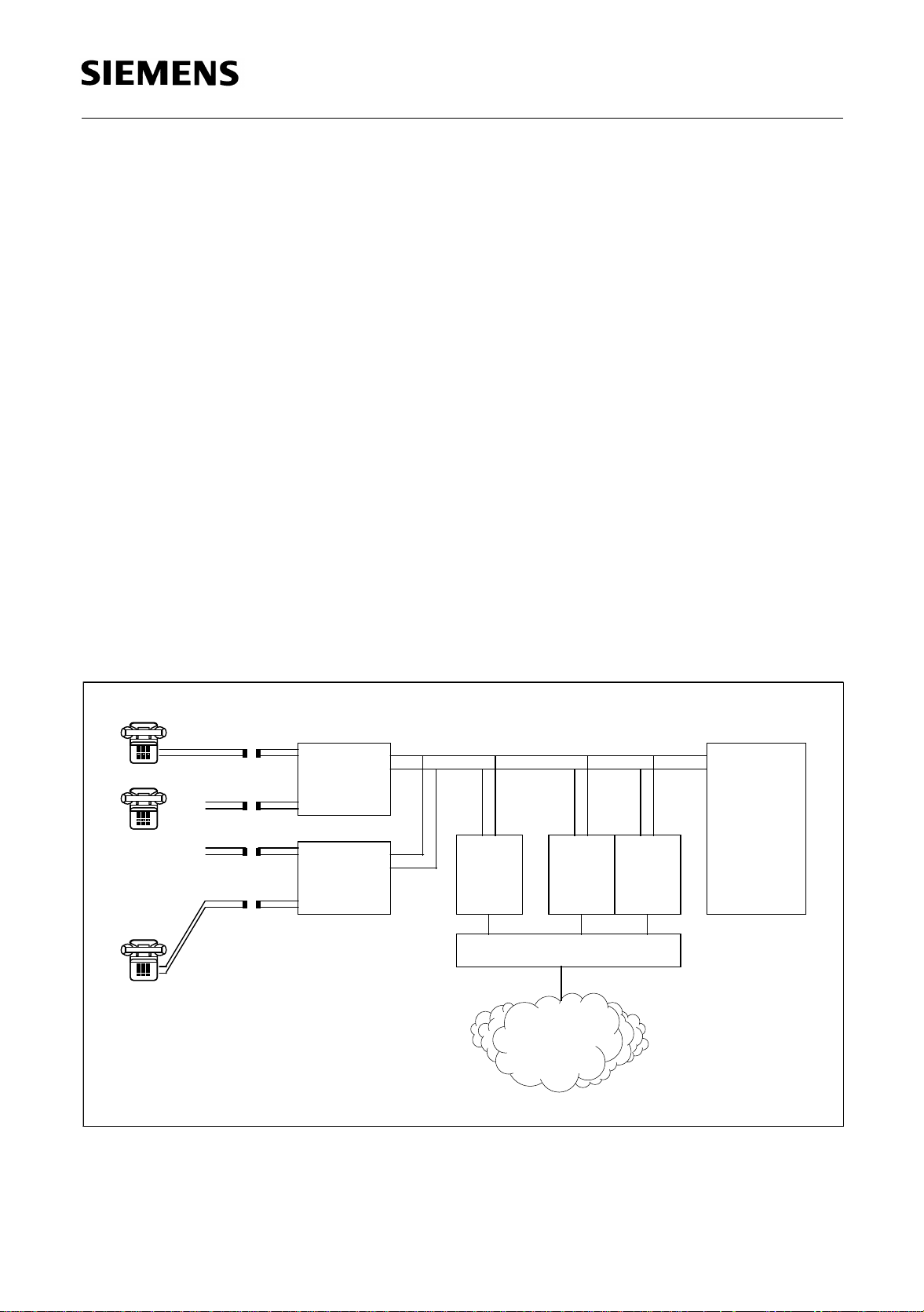
1.6.5 Internet Telephone Access in Line Card
Figure 8 sho ws an internet telephone acc ess implemented in an ana log line card of a
common tip/ring line. There is no ne ed for the user to buy a special in ternet telephon e.
With his old equipment he can use the internet f or rate-reduced calls to overs eas or to
connect to a “true” internet telephone. At the beginning or even before a new call the user
may select between th e “standard” t arif via the switchin g network and a “reduced rate”
tarif transferring speech via a packetized network such as internet.
Since the JADE AN does the voice compression/decompression complying to ITU-T
G.723 standard, it can connect to any other telepho ne using the same standard (e. g.
Microsoft Netmeeting).
The example below shows a line card with 8 subs cribers. The number of JAD E AN to
connect to the i nternet may be sele cted b etween 1 a nd 8 - depen ding o n the stat istica l
usage of this kind of connection.
Alternatively, an internet access with voice compression can also be implemented in the
switching network. This may offer an ev en better stat istical dis tribution, thu s optimizin g
the number of gateways needed.
.
.
.
.
.
.
Line Card
SICOFI-4
Siemens
PEB 2465
SICOFI-4
Siemens
PEB 2465
DU
DD
JADE AN
Siemens
PSB 7230
G.723
A-/u-law
or 16-bit
linear
...
Internet Gateway
Internet
A-/u-law
or 16-bit
linear
JADE AN
Siemens
PSB 7230
G.723 G.723
JADE AN
Siemens
PSB 7230
A-/u-law
or 16-bit
linear
Switching
Network
1
4
5
8
Figure 8
Semiconductor Group 22 Data Sheet 1998-07-01

PSB 7230
Introduction
The same principle may also be used for ISDN lin es, thus connecting common ISD N
telephones to internet phones like Microsoft Netmeeting or using the internet for
rate-reduced overseas connections.
Demonstration Board Designs
For Demonstration board designs containing the mentioned components please contact
Siemens.
Semiconductor Group 23 Data Sheet 1998-07-01
PSB 7230
General Architecture and Functions
2 General Architecture and Functions
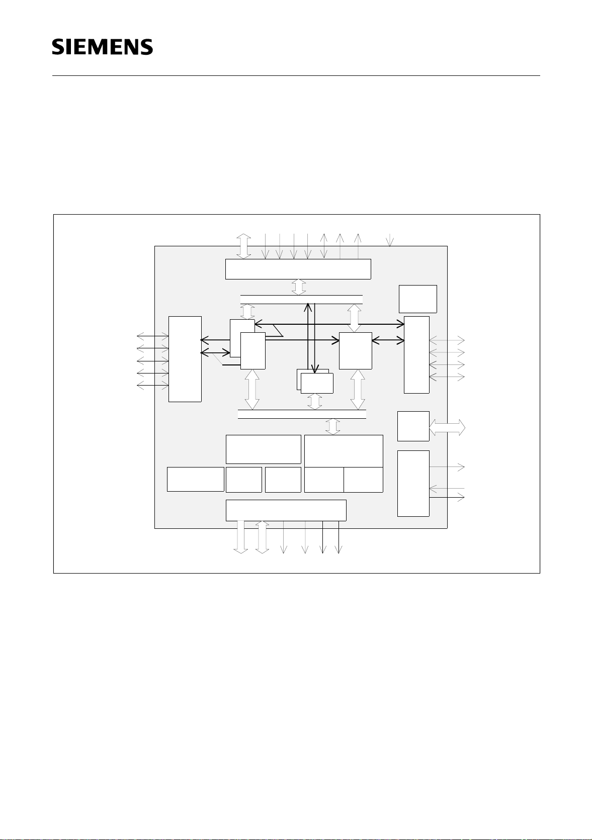
2.1 Architecture
Figure 9 shows a sketch of the PSB 7230 architecture with its most important functional
modules.
SCLK
SR
ST
RFS
TFS
Serial
Audio
I/F
Config/Control
Registers
AD(0:7) WR#RD# AL E
CS#
Parallel Host Interface
Audio
Rec 1
Trm 1
32 KW program
ROM
8 KW data
X-ROM
External Memory Interface
2 KW data
X-RAM
SIO
Mailbo x
256-byt es
1 KW data
X-RAM
INTR#
Channels
DSP
Co re
INT#
Serial
Data
1 KW data
Y-RAM
Reset
Mon, C/I
Control
IOM/
PCM
GPIO
I/F
BRG
clock
gen
DD
DU
DCL
GP(0:3)
CL K O
XTAL1
XTAL2
CA (0:15) CD(0:1 5) CWR#CRD# CD S#CP S#
Figure 9
The audio processing of the PSB 7230 is based on a 16-bit fixed point DSP core, SPCF
(Signal Processor Core Fast).
The Clock Generator is responsible for gene rating the internal clocks for the SPC. A
Baud Rate Generator provides an output clock of programmable rate.
The Parallel Host Interface is used to control the circuit through an associated host via
interrupt handshake procedures. Alternatively, the circuit can be controlled via the Serial
Audio Interface, thus enabling stand-alone applications to be implemented.
Communication between the Host, if used, and the DSP is interrupt supported, via a fullduplex 64-byte on-chip Communication Memory Mailbox.
Semiconductor Group 24 Data Sheet 1998-07-01

PSB 7230
General Architecture and Functions
One receive and one transmit audio channel are provided. They are input/output on the
ISDN Oriented Modular (IOM-2) or the Serial Audio Interface (SAI) interfaces in
individually programmable time-slots. These channels are accessed from the DSP and/
or the Parallel Host Interface.
The Serial Data Controller chann els can be serviced by the DSP or the Parallel Host
Interface. The serial d ata for the serial d ata controlle r is loc ated in p rogramma ble time slots on IOM-2 and/or SAI.
Semiconductor Group 25 Data Sheet 1998-07-01
PSB 7230
General Architecture and Functions
2.2 Functions
2.3 Summary of the Functions
The main functions implemented by the PSB 7230 are:
– G.723 V5.1 Compression/Decompression (6.3, 5.3 Kbit/s)
– G.711 Compression/Decompression (64 Kbit/s)
– Accepts/outputs uncompressed audio 8-bit PCM A/µ law or 16-bit linear format
– Uncompressed/compressed audio switchable between different interface
combinations (IOM/Serial Audio Interface, IOM/Host, Host/Host)
– Inband controlled H.221/H.223 oriented audio protocol, e.g. for direct serial
connection to Videocodec (VCP of 8 × 8 Inc., formerly IIT Inc.)
– Outband controlled audio protocol with optimized data rate
– Stable reaction on interrupt handshake timing violations of e.g. a slow host
®
(Windows
PC)
Details about these functions are given in Chapter 2.3.1.
For more details on the hardware (n ecess ary for a better und erstandi ng of som e of the
topics described in the presen t chapter), pleas e refer to the other cha pters of this Data
Sheet.
2.3.1 Audio Functions and Supplementary Features
General
The uncompressed/compressed audio is applied to the interfaces as follows:
Table 9
Uncompressed Audio Compressed Audio
IOM-2 (transparent) SAI (H.221/223 oriented audio protocol or
transparent)
IOM-2 (transparent) Host IF (interrupt handshake protocol with
minimized interrupt load for the host)
Host IF (interrupt handshake protocol) Host IF (interrupt handshake protocol)
“Transparent” means that data is received/transmitted in a time-slot without protocol.
Semiconductor Group 26 Data Sheet 1998-07-01

PSB 7230
General Architecture and Functions
Full Duplex G.711 Encoding/Decoding of one Audio Channel
Audio coding according to ITU-T G.711 recom mendati on using Puls e Co de Modulat ion
(PCM, 64 Kbit/s). A logarithmic function is used for coding of 8 kHz audio samples, thus
offering a nearly con stant S/N over the whole amplitude range . Two different laws are
defined known as A- and µ-law.
Full Duplex G.723 Encoding/Decoding of one Audio Channel
Audio coding according to ITU-T G.723 recommendation using Multipulse Maximum
Likelihood Quantization (MP-MLQ, 6.3 Kbit/s) or Algebraic Code Excited Linear
Prediction (ACELP, 5.3 Kbit/s). The high pass filter and the pos tfilter of the G.723 may
be independently switched on or off. The implementation complies with the newest ITU-T
C-Code V5.1 and contains Voice Acti vity Detection (VAD), Comfort Noise Generation
(CNG) and Discontinous Transmission (DTX).
Serial H.221/223 Oriented Audio Protocol.
The PSB 7230 supports a serial H.221/223 oriented inband controlled audio protocol for
direct connection to a Videocodec (e.g. VCP of 8 × 8 Inc.), which means the control data
for compression mode, volume etc. is sent in a header preceeding the compressed data.
This protocol provides an outband synchronization of the audio bit streams by using
block structures for the compressed audio data.
Semiconductor Group 27 Data Sheet 1998-07-01
PSB 7230
Interfaces and Memory Organization
3 Interfaces and Memory Organization
3.1 Interfaces
3.1.1 IOM-2 Interface
Electrical interface
The IOM-2 interface is a 4-wire interface with two data lines (DD and DU, programmable
open drain or push-pul l), a data clock line (DCL inp ut/output) and a frame sync s ignal
(FSC input/output). The data clock is by def ault equal to twice the data rate (“Double
rate”). However, DCL may be set equal to the data rate (“Single rate”) by programming.
In terminal applications , the bit rate on the interface is n ormally 768 Kbit/s, in line card
applications it is 2048 Kbit/s (for details, see IOM-2 Interface Reference Guide).
However, the data rat e may be different (between 16 Kbit/s and 4. 096 Mbit/s and the
DCL rate correspondin gly between 16 kHz and 4.096 MHz), since the interfa ce can b e
considered as a general purpose TDM (Time-Division Multiplex) highway.
The total number of time slots on the interface is not explicitly programmed: instead, the
FSC signal (at repetition rate 8 kHz) always marks the TDM ph ysical frame begin ning.
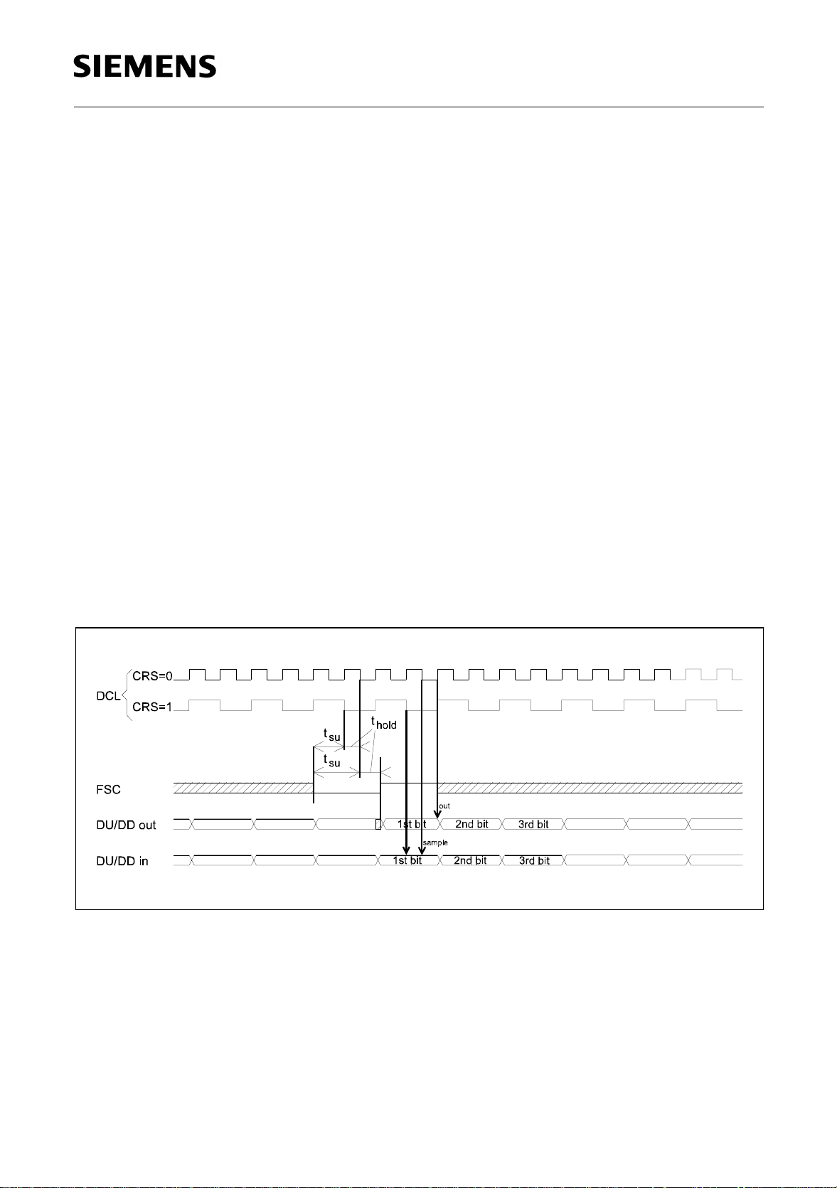
See Figure 10 for both IOM clock rates (CRS = 0/1).
Figure 10
Semiconductor Group 28 Data Sheet 1998-07-01

PSB 7230
Interfaces and Memory Organization
DCL Bits on DU/DD are clocked out with the rising edge of DCL and
latched in with the falling edge of DCL. Frequency 16 kHz to
4.096 MHz.
FSC (8 kHz) Marks the beginning of the physical frame on DU and DD. The first
bit in the frame is output after the rising edge of FSC. The first bit in
the frame is latched in with the first falling edge after FSC has gone
“high” if CRS = 1, or after the second edge (at 3/4) if CRS = 0.
Channels
The following channe ls may be programmed on the IOM-2 in terfac e: one receive audio
channel, one transmit audio channel, one Monitor channel, two C/I channels, one
receive and one transmit data channel:
Audio receive channel
Audio transmit channel
Independently programmable on DD or
DU, with progr amma ble locat ion s (sta rt at
bit 1 … 512) and lengths (1 … 32 bits)
w.r.t. FSC
Monitor channel Programmable on DD(in)/DU(out) or
DD(out)/DU(in), with programmable
time-slot (3rd byte in multiplex 0 … 15)
after FSC
Two C/I channels Programmable on DD(in)/DU(out) or
DD(out)/DU(in), with programmable length
(4 or 6 bits) and position (4th byte in
multiplex 0 … 15) after FSC
Data receive and transmit channels Independently programmable on DD or
DU, with progr amma ble locat ion s (sta rt at
bit 1 … 512) and lengths (1 … 256 bits)
w.r.t. FSC
The transfer of voice samples is performed with the help of an interrupt with repetit ion
rate 8 kHz derived from the FSC signal. A do uble - buff ered re gis ter is provided for each
channel, accessible from the DSP and from the parallel host interface. The double
buffered register ensures th at enough time is always provided for reading and writing
data before an overflow/underflow occurs, independent of the location of the time-slots.
Alternatively, the audio samples can be transferred between the DSP or Host and IOM-2
by using an interrupt generated when a programmable number (1 … 32) of bits are
shifted out (number independent of the time-slot length on the line).
Outside the time slo ts w here tran smiss ion takes place t he DU and D D lin es are in high
impedance.
Semiconductor Group 29 Data Sheet 1998-07-01
PSB 7230
Interfaces and Memory Organization
3.1.2 Serial Audio Interface
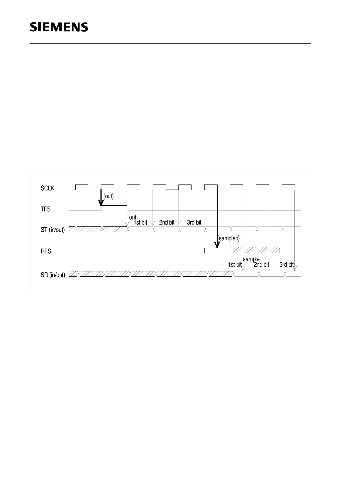
The Serial Audio Interface is a generic 5-line serial interface with the following lines:
SCLK Serial bit clock Input or Output
SR Serial Receive Input/Output
ST Serial Transmit Input/Output
RFS Receive Frame Sync Input or Output
TFS Transmit Frame Sync Input or Output.
Figure 11 shows an example where RFS is input and TFS is output.
Figure 11
Semiconductor Group 30 Data Sheet 1998-07-01