

Siemens PSB21911, PSF21911 Datasheet

ICs for Communications
ISDN Echocancellation Circuit for Terminal Applications
IEC-Q TE
PSB 21911 Version 5.2
PSF 21911 Version 5.2
Data Sheet 11.97
DS 1

PSB 21911
Revision History: Original Version: 11.97
Previous Releases: None
Page Subjects (changes since last revision)
For questions on technology, delivery and prices please con tact the Semiconductor
Group Offices in Germany or the Siemens Companies and Representatives worldwide:
see our webpage at http://www.siemens.de/Semiconductor/address/address.htm.
Edition 11.97
Published by Siemens AG,
HL TS,
Balanstraße 73,
81541 München
©
Siemens AG 28.11.97.
All Rights Reserved.
Attention please!
As far as patents or other rights of third parties are concerned, liability is only assumed for components, not for
applications, processes and circui ts implemented within component s or assemblies.
The information describes the type of component and s hall not be considered as assured ch aracteristics.
Terms of delivery and rights to change design reserved.
Due to tec hnical requirements components may contain dangerous substances. For information on the types in
question please contact your nearest Siemens Off ice, Semiconductor Group.
Siemens AG is an approved CECC manufacturer.
Packing
Please use the recycling operators known to you. We can also help you – get in touch with your nearest sales
office. By agreement we will take packing material back, if it is sorted. You must bear the costs of transport.
For pac king mat erial that is ret urned to us unsorte d or wh ich we a re not oblig ed to a ccept, we shal l have to in v oice
you for any costs incurred.
Components used in life-support devices or systems must be expressly authorized for such purpose!
Criti cal compon ents1 of the Semiconductor Group of Siemens AG, may only be used in life-support devices or
systems2 with the express written approval of the Semiconductor Group of Siemens AG.
1 A critical component is a component used in a life-support devi ce or system whose failure can reasonably be
expected t o ca use t he f ail u re o f th at l ife- s upp ort devi ce o r s ys tem, or to af fe ct i t s saf et y or ef fe ct ive ness of t hat
device or system.
2 Life support devices or systems are intended (a) to be implanted in the human body, or (b) to support and/or
maintain and sustain human life. If they fail, it is reasonable to assume that the health of the user may be endangered.

PSB 21911
PSF 21911
Table of Contents Page
1 Overview
1.1 Features . . . . . . . . . . . . . . . . . . . . . . . . . . . . . . . . . . . . . . . . . . . . . . . . . . .9
1.2 Logic Symbol µP Mode . . . . . . . . . . . . . . . . . . . . . . . . . . . . . . . . . . . . . . .10
1.3 Logic Symbol Stand-Alone Mode . . . . . . . . . . . . . . . . . . . . . . . . . . . . . . .11
1.4 Pin Configuration . . . . . . . . . . . . . . . . . . . . . . . . . . . . . . . . . . . . . . . . . . . .12
1.5 Pin Definitions and Functions . . . . . . . . . . . . . . . . . . . . . . . . . . . . . . . . . .13
1.6 Microprocessor Bus Interface (Overview) . . . . . . . . . . . . . . . . . . . . . . . . .21
1.7 System Integration . . . . . . . . . . . . . . . . . . . . . . . . . . . . . . . . . . . . . . . . . . .22
1.7.1 ISDN PC Adapter Card . . . . . . . . . . . . . . . . . . . . . . . . . . . . . . . . . . . . . . .22
1.7.2 ISDN Stand -Alone Termi nal with POTS Interface . . . . . . . . . . . . . . . . . . .23
1.7.3 ISDN Feat ure Phone . . . . . . . . . . . . . . . . . . . . . . . . . . . . . . . . . . . . . . . . .24
1.7.4 ISDN-Modem PC Card . . . . . . . . . . . . . . . . . . . . . . . . . . . . . . . . . . . . . . .25
2 Functional Description
2.1 Operating Modes . . . . . . . . . . . . . . . . . . . . . . . . . . . . . . . . . . . . . . . . . . . .26
2.2 Device Architecture . . . . . . . . . . . . . . . . . . . . . . . . . . . . . . . . . . . . . . . . . .28
2.3 IOM-2 Interface . . . . . . . . . . . . . . . . . . . . . . . . . . . . . . . . . . . . . . . . . . . . .30
2.3.1 IOM-2 Frame Structure . . . . . . . . . . . . . . . . . . . . . . . . . . . . . . . . . . . . . . .30
2.3.2 IOM-2 Command / Indication Channels . . . . . . . . . . . . . . . . . . . . . . . . . .34
2.3.3 IOM-2 Monitor Channel . . . . . . . . . . . . . . . . . . . . . . . . . . . . . . . . . . . . . . .35
2.3.4 Activation/Deactiva tion of IOM-2 Clocks . . . . . . . . . . . . . . . . . . . . . . . . . .37
2.3.5 Superframe Marker . . . . . . . . . . . . . . . . . . . . . . . . . . . . . . . . . . . . . . . . . .38
2.3.6 IOM-2 Output Driver Selection . . . . . . . . . . . . . . . . . . . . . . . . . . . . . . . . .38
2.4 Microprocessor Interface . . . . . . . . . . . . . . . . . . . . . . . . . . . . . . . . . . . . . .39
2.4.1 Microprocessor Clock Output . . . . . . . . . . . . . . . . . . . . . . . . . . . . . . . . . .39
2.4.2 Watchdog Timer . . . . . . . . . . . . . . . . . . . . . . . . . . . . . . . . . . . . . . . . . . . .39
2.5 U-Transceiver . . . . . . . . . . . . . . . . . . . . . . . . . . . . . . . . . . . . . . . . . . . . . .40
2.5.1 U-Frame Structure . . . . . . . . . . . . . . . . . . . . . . . . . . . . . . . . . . . . . . . . . . .42
2.5.2 EOC-Processor and MON-0 . . . . . . . . . . . . . . . . . . . . . . . . . . . . . . . . . . .51
2.5.3 Maintenance (MON-1) . . . . . . . . . . . . . . . . . . . . . . . . . . . . . . . . . . . . . . . .54
2.5.4 O verh ead Bits (MON-2) . . . . . . . . . . . . . . . . . . . . . . . . . . . . . . . . . . . . . . .56
2.5.5 Local Functions (MON-8) . . . . . . . . . . . . . . . . . . . . . . . . . . . . . . . . . . . . .59
2.5.6 State Machine Notation Rules . . . . . . . . . . . . . . . . . . . . . . . . . . . . . . . . . .62
2.5.7 State Machine . . . . . . . . . . . . . . . . . . . . . . . . . . . . . . . . . . . . . . . . . . . . . .63
2.5.8 C/I Codes . . . . . . . . . . . . . . . . . . . . . . . . . . . . . . . . . . . . . . . . . . . . . . . . . .74
2.5.9 Layer 1 Loop-Backs . . . . . . . . . . . . . . . . . . . . . . . . . . . . . . . . . . . . . . . . . .76
2.5.10 Analog Line Port . . . . . . . . . . . . . . . . . . . . . . . . . . . . . . . . . . . . . . . . . . . .78
2.6 Access to IOM-2 Channel s . . . . . . . . . . . . . . . . . . . . . . . . . . . . . . . . . . . .81
2.6.1 B-Channel Access . . . . . . . . . . . . . . . . . . . . . . . . . . . . . . . . . . . . . . . . . . .82
2.6.2 D-Channel Access . . . . . . . . . . . . . . . . . . . . . . . . . . . . . . . . . . . . . . . . . . .82
2.6.3 C/I Channel Access . . . . . . . . . . . . . . . . . . . . . . . . . . . . . . . . . . . . . . . . . .83
2.6.4 Monitor Channel Access . . . . . . . . . . . . . . . . . . . . . . . . . . . . . . . . . . . . . .84
2.7 S/G Bit and BAC Bit in TE Mode . . . . . . . . . . . . . . . . . . . . . . . . . . . . . . .89
. . . . . . . . . . . . . . . . . . . . . . . . . . . . . . . . . . . . . . . . . . . . . . . . . . .8
. . . . . . . . . . . . . . . . . . . . . . . . . . . . . . . . . . . . . .26
Semiconductor Group 3 11.97

PSB 21911
PSF 21911
2.7.1 Applications with ELIC on the Linecard (PBX) . . . . . . . . . . . . . . . . . . . . .90
2.8 Reset . . . . . . . . . . . . . . . . . . . . . . . . . . . . . . . . . . . . . . . . . . . . . . . . . . . . .93
2.9 Power Controller Interface . . . . . . . . . . . . . . . . . . . . . . . . . . . . . . . . . . . . .94
3 Operational Description
. . . . . . . . . . . . . . . . . . . . . . . . . . . . . . . . . . . . .97
3.1 C/I Channel Programming . . . . . . . . . . . . . . . . . . . . . . . . . . . . . . . . . . . . .97
3.2 Monitor Channel Programming . . . . . . . . . . . . . . . . . . . . . . . . . . . . . . . . .98
3.3 Layer 1 Activation/Deactivation . . . . . . . . . . . . . . . . . . . . . . . . . . . . . . . .100
3.4 External Circuitry . . . . . . . . . . . . . . . . . . . . . . . . . . . . . . . . . . . . . . . . . . .109
3.4.1 Power Supply Blocking Recommendation . . . . . . . . . . . . . . . . . . . . . . . .109
3.4.2 U-Interface . . . . . . . . . . . . . . . . . . . . . . . . . . . . . . . . . . . . . . . . . . . . . . . .110
3.4.3 Oscillator Circuit . . . . . . . . . . . . . . . . . . . . . . . . . . . . . . . . . . . . . . . . . . .111
4 Register Description
. . . . . . . . . . . . . . . . . . . . . . . . . . . . . . . . . . . . . . .112
4.1 Interrupt Structure . . . . . . . . . . . . . . . . . . . . . . . . . . . . . . . . . . . . . . . . . .114
4.1.1 Monitor-Channel Interrupt Logic . . . . . . . . . . . . . . . . . . . . . . . . . . . . . . .115
4.2 Registers . . . . . . . . . . . . . . . . . . . . . . . . . . . . . . . . . . . . . . . . . . . . . . . . .116
5 Electrical Characteristics
. . . . . . . . . . . . . . . . . . . . . . . . . . . . . . . . . . .130
5.1 Absolute Maximum Ratings . . . . . . . . . . . . . . . . . . . . . . . . . . . . . . . . . . .130
5.2 Power Consumption . . . . . . . . . . . . . . . . . . . . . . . . . . . . . . . . . . . . . . . .132
5.3 DC Characteristics . . . . . . . . . . . . . . . . . . . . . . . . . . . . . . . . . . . . . . . . . .133
5.4 AC Characteristics . . . . . . . . . . . . . . . . . . . . . . . . . . . . . . . . . . . . . . . . . .136
5.4.1 Parallel Microprocessor Interface Timing . . . . . . . . . . . . . . . . . . . . . . . .136
5.4.2 Serial Microprocessor Interface Timing . . . . . . . . . . . . . . . . . . . . . . . . . .140
5.4.3 IOM-2 Interface Timing . . . . . . . . . . . . . . . . . . . . . . . . . . . . . . . . . . . . . .142
6 Package Outlines
7 External Component Sourcing
8 Glossary
. . . . . . . . . . . . . . . . . . . . . . . . . . . . . . . . . . . . . . . . . . . . . . . . .152
. . . . . . . . . . . . . . . . . . . . . . . . . . . . . . . . . . . . . . . . . .147
. . . . . . . . . . . . . . . . . . . . . . . . . . . . . . .149
Appendix
App A Jitter on IOM-2 . . . . . . . . . . . . . . . . . . . . . . . . . . . . . . . . . . . . . . . . . . . . .154
App B S/G Bit Control State Machine . . . . . . . . . . . . . . . . . . . . . . . . . . . . . . . . .155
App C Quick Reference Guide . . . . . . . . . . . . . . . . . . . . . . . . . . . . . . . . . . . . . .160
Index
IOM®, IOM®-1, IOM®-2, SIC OF I®, SICOFI®-2, SICOFI®-4, SIC OF I®-4µC, SLICOFI®, ARCOFI
ARCOFI®-SP, EPIC®-1, EPIC®-S, ELIC®, IPAT®-2, ITAC®, ISAC®-S, ISAC®-S TE, ISAC®-P, ISAC®-P TE, IDEC®,
SICAT®, OCTAT®-P, QUA T®-S are registered trademarks of Siemens AG.
MUSAC™-A, FALC™54, IWE™, SARE™, UTPT™, ASM™, ASP™, DigiTape™ are trademarks of Siemens AG.
2
Purchase of Sie mens
2
I
the
C-syst em provided t he system conf orms to the
I
C components conveys a license under the Philips’
2
I
C specifications defined by Philips. Copyright Philips 1983.
2
I
C patent to use the components in
®
, ARCOFI®-BA,
Semiconductor Group 4 11.97

PSB 21911
PSF 21911
List of Figures Page
Figure 1: Stand-Alone Mode (left) and µP Mode (right). . . . . . . . . . . . . . . . . . . . . . . 8
Figure 2: Logic Sym bol µP Mode . . . . . . . . . . . . . . . . . . . . . . . . . . . . . . . . . . . . . . . 10
Figure 3: Logic Symbol Stand-Alone Mode . . . . . . . . . . . . . . . . . . . . . . . . . . . . . . . 11
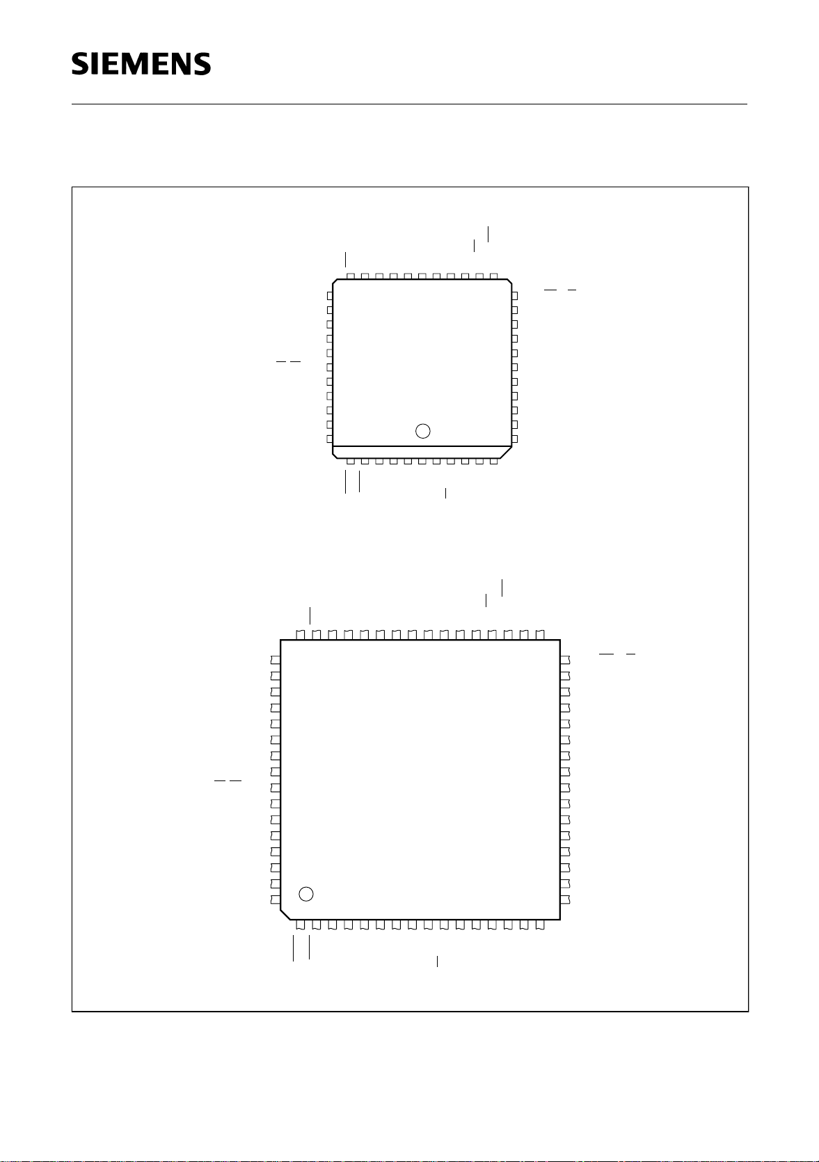
Figure 4: Pin Configuration P-LCC-44 and T-QFP-64 Package (top view) . . . . . . . 12
Figure 5: ISDN PC Adapter Card . . . . . . . . . . . . . . . . . . . . . . . . . . . . . . . . . . . . . . . 22
Figure 6: ISDN Stand-Alone Terminal with POTS Interface . . . . . . . . . . . . . . . . . . 23
Figure 7: ISDN Feat ure Phone . . . . . . . . . . . . . . . . . . . . . . . . . . . . . . . . . . . . . . . . 24
Figure 8: ISDN-Modem PC Card. . . . . . . . . . . . . . . . . . . . . . . . . . . . . . . . . . . . . . . 25
Figure 9: IEC-Q TE Device Architecture (µP Mode) . . . . . . . . . . . . . . . . . . . . . . . . 28
Figure 10: IEC-Q TE Device Architecture (Stand-Alone Mode). . . . . . . . . . . . . . . . . 29
Figure 11: IOM-2 Clocks and Data Lines. . . . . . . . . . . . . . . . . . . . . . . . . . . . . . . . . . 30
Figure 12: Basic Channel Structure of IOM-2 . . . . . . . . . . . . . . . . . . . . . . . . . . . . . . 31
Figure 13: Definition of the IOM-2 Frame in TE Mode. . . . . . . . . . . . . . . . . . . . . . . . 32
Figure 14: Definition of the IOM-2 Frame in NT Mode. . . . . . . . . . . . . . . . . . . . . . . . 33
Figure 15: Deactivation of the IOM-2 Clocks. . . . . . . . . . . . . . . . . . . . . . . . . . . . . . . 37
Figure 16: U-Transceiver Block Diagram. . . . . . . . . . . . . . . . . . . . . . . . . . . . . . . . . . 41
Figure 17: CRC-Process . . . . . . . . . . . . . . . . . . . . . . . . . . . . . . . . . . . . . . . . . . . . . . 45
Figure 18: Block Error Counter Test . . . . . . . . . . . . . . . . . . . . . . . . . . . . . . . . . . . . . 48
Figure 19: Scrambler / Descrambler Algorithms . . . . . . . . . . . . . . . . . . . . . . . . . . . . 49
Figure 20: EOC-Processor: Auto Mode, Transparent Mode . . . . . . . . . . . . . . . . . . . 51
Figure 21: State Diagram Notation U-Transceiver. . . . . . . . . . . . . . . . . . . . . . . . . . . 62
Figure 22: State Transition Diagram . . . . . . . . . . . . . . . . . . . . . . . . . . . . . . . . . . . . . 64
Figure 23: Test Loop-Backs Supported by the IEC-Q TE . . . . . . . . . . . . . . . . . . . . . 76
Figure 24: DAC-Output for a Single Pulse . . . . . . . . . . . . . . . . . . . . . . . . . . . . . . . . . 79
Figure 25: Pulse Mask for a Single Positive Pulse . . . . . . . . . . . . . . . . . . . . . . . . . . 80
Figure 26: Access to IOM-2 Channels (µP mode). . . . . . . . . . . . . . . . . . . . . . . . . . . 81
Figure 27: Procedure for the D-Channel Processing. . . . . . . . . . . . . . . . . . . . . . . . . 83
Figure 28: C/I Channel Access . . . . . . . . . . . . . . . . . . . . . . . . . . . . . . . . . . . . . . . . . 84
Figure 29: Monitor Channel Access Directions . . . . . . . . . . . . . . . . . . . . . . . . . . . . . 85
Figure 30: Monitor Channel Protocol. . . . . . . . . . . . . . . . . . . . . . . . . . . . . . . . . . . . . 87
Figure 31: D-Channel Request by the Terminal . . . . . . . . . . . . . . . . . . . . . . . . . . . . 92
Figure 32: Reset Sources . . . . . . . . . . . . . . . . . . . . . . . . . . . . . . . . . . . . . . . . . . . . . 93
Figure 33: Sampling of Interrupts . . . . . . . . . . . . . . . . . . . . . . . . . . . . . . . . . . . . . . . 96
Figure 34: Example: C/I-Channel Use (all data values hexadecimal) . . . . . . . . . . . . 97
Figure 35: Complete Activation Initiated by LT . . . . . . . . . . . . . . . . . . . . . . . . . . . . 101
Figure 36: Complete Activation Initiated by TE . . . . . . . . . . . . . . . . . . . . . . . . . . . . 102
Figure 37: Complete Deactivation. . . . . . . . . . . . . . . . . . . . . . . . . . . . . . . . . . . . . . 103
Figure 38: U Only Activation . . . . . . . . . . . . . . . . . . . . . . . . . . . . . . . . . . . . . . . . . . 104
Figure 39: LT Initiated Activation with U-Interface Active . . . . . . . . . . . . . . . . . . . . 105
Figure 40: TE-Activation with U Active and Exchange Control (case 1) . . . . . . . . . 106
Figure 41: TE-Activation with U Active and no Exchange Control (case 2). . . . . . . 107
Figure 42: Deactivation of S/T Only. . . . . . . . . . . . . . . . . . . . . . . . . . . . . . . . . . . . . 108
Semiconductor Group 5 11.97

PSB 21911
PSF 21911
Figure 43: Power Supply Blocking. . . . . . . . . . . . . . . . . . . . . . . . . . . . . . . . . . . . . . 109
Figure 44: U-Interface Hybrid Circuit. . . . . . . . . . . . . . . . . . . . . . . . . . . . . . . . . . . . 110
Figure 45: Crystal Oscillator or External Clock Source . . . . . . . . . . . . . . . . . . . . . . 111
Figure 46: Interrupt Structure. . . . . . . . . . . . . . . . . . . . . . . . . . . . . . . . . . . . . . . . . . 114
Figure 47: Test Condition for Maximum Input Current. . . . . . . . . . . . . . . . . . . . . . . 131
Figure 48: U-Transceiver Input Current. . . . . . . . . . . . . . . . . . . . . . . . . . . . . . . . . . 131
Figure 49: Maximum Sinusoidal Ripple on Supply Voltage. . . . . . . . . . . . . . . . . . . 135
Figure 50: Input/Output Waveform for AC Tests. . . . . . . . . . . . . . . . . . . . . . . . . . . 136
Figure 51: Siemens/Intel Read Cycle . . . . . . . . . . . . . . . . . . . . . . . . . . . . . . . . . . . 136
Figure 52: Siemens/Intel Write Cycle . . . . . . . . . . . . . . . . . . . . . . . . . . . . . . . . . . . 137
Figure 53: Siemens/Intel Multiplexed Address Timing. . . . . . . . . . . . . . . . . . . . . . . 137
Figure 54: Siemens/Intel Non-Multiplexed Address Timing. . . . . . . . . . . . . . . . . . . 137
Figure 55: Motorola Read Timing . . . . . . . . . . . . . . . . . . . . . . . . . . . . . . . . . . . . . . 138
Figure 56: Motorola Write Cycle . . . . . . . . . . . . . . . . . . . . . . . . . . . . . . . . . . . . . . . 138
Figure 57: Motorola Non-Multiplexed Address Timing. . . . . . . . . . . . . . . . . . . . . . . 138
Figure 58: Serial µP Interface Mode Write. . . . . . . . . . . . . . . . . . . . . . . . . . . . . . . . 140
Figure 59: Serial µP Interface Mode Read . . . . . . . . . . . . . . . . . . . . . . . . . . . . . . . 140
Figure 60: IOM-2 Timing in NT Mode . . . . . . . . . . . . . . . . . . . . . . . . . . . . . . . . . . . 142
Figure 61: Dynamic Characteristics of Power Controller Write Access. . . . . . . . . . 144
Figure 62: Dynamic Characteristics of Power Controller Read Access. . . . . . . . . . 144
Figure 63: Reset Signal. . . . . . . . . . . . . . . . . . . . . . . . . . . . . . . . . . . . . . . . . . . . . . 146
Figure 64: S/G Bit State Machine Notation . . . . . . . . . . . . . . . . . . . . . . . . . . . . . . . 155
Figure 65: State machine (part 1) . . . . . . . . . . . . . . . . . . . . . . . . . . . . . . . . . . . . . . 156
Figure 66: State machine (part 2) . . . . . . . . . . . . . . . . . . . . . . . . . . . . . . . . . . . . . . 157
Figure 67: State machine (part 3) . . . . . . . . . . . . . . . . . . . . . . . . . . . . . . . . . . . . . . 158
Figure 68: U-Transceiver State Diagram. . . . . . . . . . . . . . . . . . . . . . . . . . . . . . . . . 161
Semiconductor Group 6 11.97

PSB 21911
PSF 21911
List of Tables Page
Table 1: Microprocessor Bus Interface. . . . . . . . . . . . . . . . . . . . . . . . . . . . . . . . . . .21
Table 2: Mo des of Oper ation (µP and Stand-Alone Mode) . . . . . . . . . . . . . . . . . . .26
Table 3: Test Modes. . . . . . . . . . . . . . . . . . . . . . . . . . . . . . . . . . . . . . . . . . . . . . . . .27
Table 4: DOUT Driver Modes. . . . . . . . . . . . . . . . . . . . . . . . . . . . . . . . . . . . . . . . . .27
Table 5: Microprocessor Interface Modes . . . . . . . . . . . . . . . . . . . . . . . . . . . . . . . .39
Table 6: U-Frame Structure . . . . . . . . . . . . . . . . . . . . . . . . . . . . . . . . . . . . . . . . . . .43
Table 7: EO C-Codes . . . . . . . . . . . . . . . . . . . . . . . . . . . . . . . . . . . . . . . . . . . . . . . .50
Table 8: Executed EOC Commands in Auto Mode . . . . . . . . . . . . . . . . . . . . . . . . .53
Table 9: Mon-1 S/Q-Channel Commands and Indicat ions. . . . . . . . . . . . . . . . . . . .54
Table 10: Mon-1 M-Bit Commands. . . . . . . . . . . . . . . . . . . . . . . . . . . . . . . . . . . . . . .55
Table 11: MON-2 Structure . . . . . . . . . . . . . . . . . . . . . . . . . . . . . . . . . . . . . . . . . . . .56
Table 12: Control of Overhead Bits . . . . . . . . . . . . . . . . . . . . . . . . . . . . . . . . . . . . . .56
Table 13: Mon-8 Local Function Commands . . . . . . . . . . . . . . . . . . . . . . . . . . . . . . .59
Table 14: Timers. . . . . . . . . . . . . . . . . . . . . . . . . . . . . . . . . . . . . . . . . . . . . . . . . . . . .68
Table 15: U-Transceiver C/I Codes . . . . . . . . . . . . . . . . . . . . . . . . . . . . . . . . . . . . . .75
Table 16: B1/B2-Channel Data Registers . . . . . . . . . . . . . . . . . . . . . . . . . . . . . . . . .82
Table 17: D-channel data registers . . . . . . . . . . . . . . . . . . . . . . . . . . . . . . . . . . . . . .82
Table 18: S/G Processing Mode. . . . . . . . . . . . . . . . . . . . . . . . . . . . . . . . . . . . . . . . .89
Table 19: Control Structure of the S/G Bit and of the D-Channel . . . . . . . . . . . . . . .90
Table 20: Reset . . . . . . . . . . . . . . . . . . . . . . . . . . . . . . . . . . . . . . . . . . . . . . . . . . . . .93
Table 21: MON-8 and C/I-Commands . . . . . . . . . . . . . . . . . . . . . . . . . . . . . . . . . . . .94
Table 22: U-Interface Signals. . . . . . . . . . . . . . . . . . . . . . . . . . . . . . . . . . . . . . . . . .100
Table 23: Register Address Map . . . . . . . . . . . . . . . . . . . . . . . . . . . . . . . . . . . . . . .112
Table 24: Register Summary . . . . . . . . . . . . . . . . . . . . . . . . . . . . . . . . . . . . . . . . . .113
Table 25: Timing Characteristics (serial µP interface mode) . . . . . . . . . . . . . . . . . .141
Table 26: IOM-2 in NT Mode . . . . . . . . . . . . . . . . . . . . . . . . . . . . . . . . . . . . . . . . . .143
Table 27: Power Controller Interface Dynamic Characteristics . . . . . . . . . . . . . . . .145
Table 28: Reset Timing . . . . . . . . . . . . . . . . . . . . . . . . . . . . . . . . . . . . . . . . . . . . . .146
Table 29: U-Transformer Information. . . . . . . . . . . . . . . . . . . . . . . . . . . . . . . . . . . .149
Table 30: Crystal Information . . . . . . . . . . . . . . . . . . . . . . . . . . . . . . . . . . . . . . . . . .151
Table 31: State Machine Input Signals. . . . . . . . . . . . . . . . . . . . . . . . . . . . . . . . . . .159
Table 32: State Machine Output Signals . . . . . . . . . . . . . . . . . . . . . . . . . . . . . . . . .159
Table 33: U-Transceiver C/I Codes . . . . . . . . . . . . . . . . . . . . . . . . . . . . . . . . . . . . .162
Semiconductor Group 7 11.97
PSB 21911
PSF 21911
Overview
1 Overview
The PSB 21911, IEC-Q TE Version 5.2, is a specific derivative of the PEB 2091, IEC-Q
for terminal and small PBX applications. It features all necessary functions required for
NTs and terminal applications like PC add-on cards and terminal adapt ers .
In stand-alone mode the PSB 21911 IEC-Q TE Version 5.2 can be used fully pin
compatible to IEC-Q V4.4 and former vers ions. In µP mode it offers a parallel or serial
microprocessor interface.
The P
rocessor Interface (PI) of the IEC-Q TE V 5.2 establishes the access of a
microprocessor between U-interface and IOM-2. It’s main function is illustrated in
figure 1
.
FSC
R
IOM -2
R
IOM -2
UU
PI
ITS10193
Figure 1 Stand-Alone Mode (left) and µP Mode (right)
In µP mode B ch annels, D channel, C/I codes and Monitor commands can either be
passed between the U-transceiver and IOM-2 directly, or they can be looped through the
µP via the PI. Any selection of "passed" or "looped" channels can be programmed via a
control register.
The µP-interface mode is en abl ed by setting the pin PMODE to "1". This pin w as not to
be connected in older versions of the IEC-Q. Its internal pul l down resistor selects the
stand-alone mode, if the pin is left open.
In stand-alone mode the IEC-Q TE is controlled exclusively vi a the IOM-2 interface and
mode selection pins.
Semiconductor Group 8 11.97
ISDN Echo cancellation Circuit fo r Terminal
PSB 21911
Applications
IEC-Q TE
Version 5.2 CMOS
1.1 Features
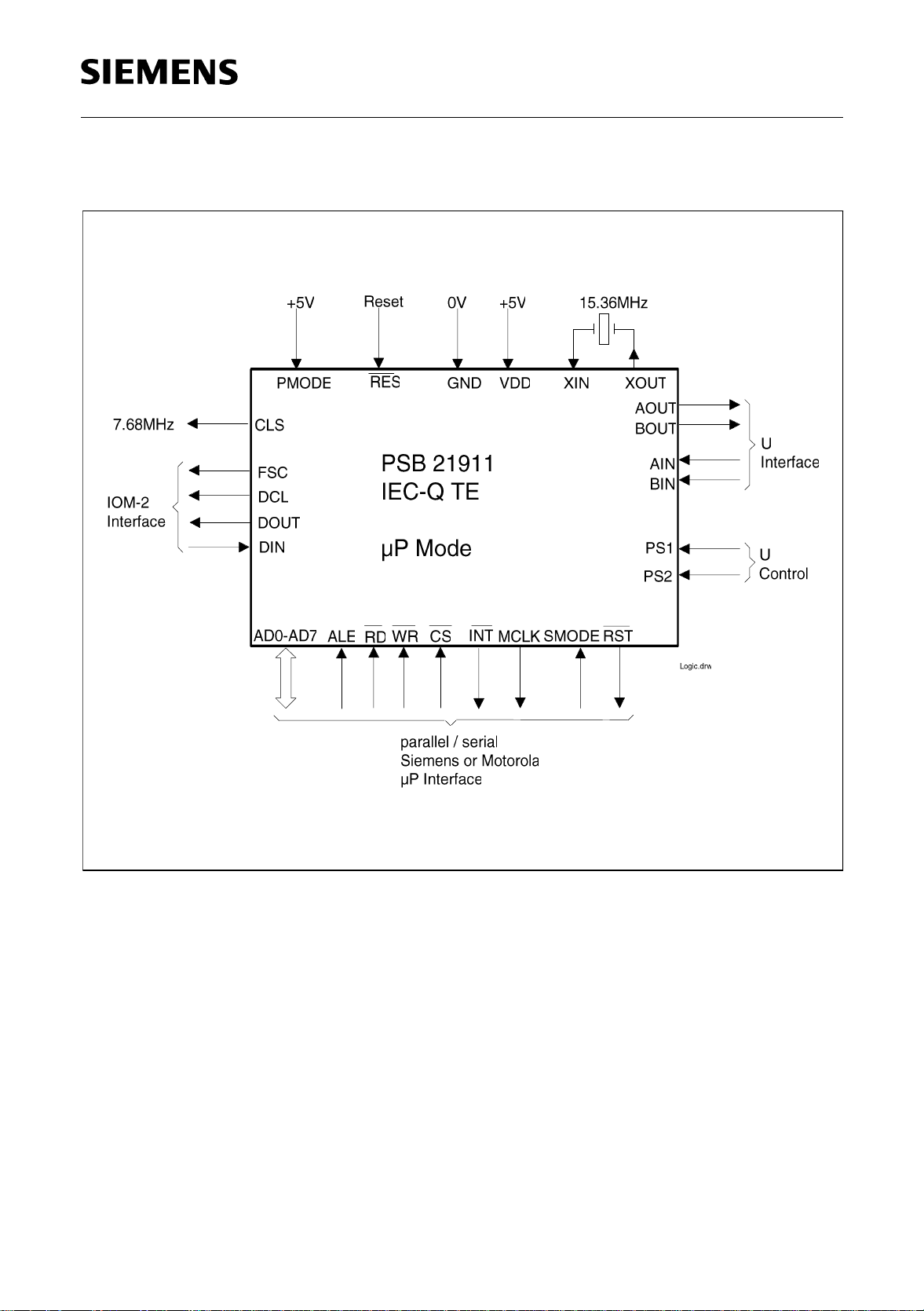
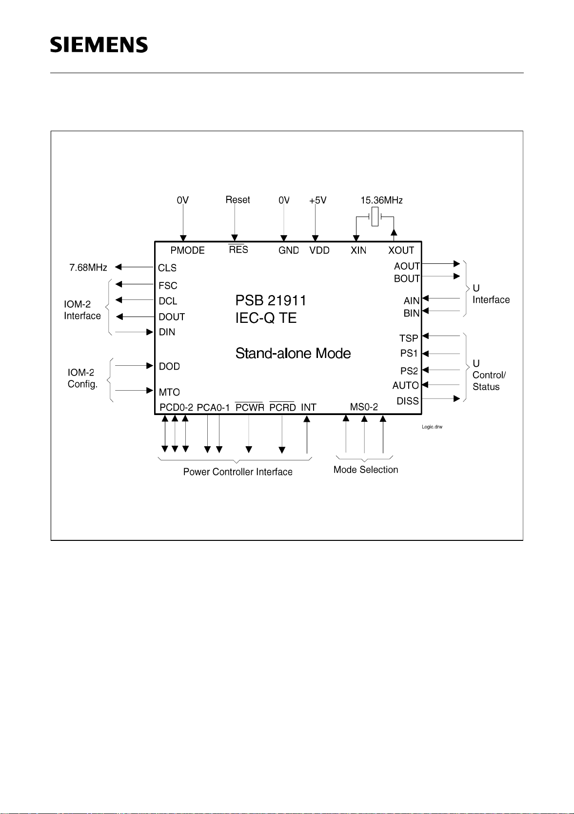
• ISDN U-transceiver with IO M-2 and optional m icro-
processor interface
• Compatible to NT modes and TE mode of
PEB 2091 IEC-Q V5.1
• Perfectly suited for terminal and TA applications
• U-interface (2B1Q) conform to ANSI T1.601, ETSI
ETR 080 and CNET ST/LAA/ELR/DNP/822:
– Meets all transmission requirements on all ANSI,
ETSI and CNET loops with margin
– Conform to British Telecom’s RC7355E
– Compliant with ETSI 10ms micro interruptio ns
• IOM-2 interface for connection of e.g. ISAC-S,
SICOFI-2/4TE, ARCOFI, ITAC, HSCX-TE, ISAR,
IPAC, 3PAC
• Pin compatible to version 4.4 in the P-LCC-44
package
P-LCC-44
T-QFP-64
In µP mode:
• Parallel or serial microprocessor interface and watchdog
• µP access to B-channels, D-channel and intercommunication channels
• µP access to IOM-2 Monitor-channels and C/I-channels
• Adjustable microcontroller clock source between 0.96MHz and 7.68MHz
• Selection between Bit clock (BCL) and Data clock (DCL)
• Supports synchronization of bas esta tions in cordl ess app licatio ns (e.g . RITL)
• Supports D-channel arbitration with ELIC linecard (e.g. PBX)
In all modes:
• Single 5 Volt power supply
• Low power CMOS technology with power down mode
Semiconductor Group 9 11.97
1.2 Logic Symbol µP Mode
PSB 21911
PSF 21911
Logic Symbol µP Mode
Figure 2 Logic Symbol µP Mode
Semiconductor Group 10 11.97
1.3 Logic Symbol Stand-Alone Mode
PSB 21911
PSF 21911
Logic Symbol Stand-Alone Mode
Figure 3 Logic Symbol Stand-Alone Mode
Semiconductor Group 11 11.97
1.4 Pin Configuration
A3/MS0
DS/RD/MTO
CDOUT/A2/MS1
CDIN/A1/MS2
MCLK/DISS
D6/AD6/PCA1
D5/AD5/PCA0
TP
FSC
DCL
CLS
RES
DOUT
29
30
31
32
33
34
35
36
37
38
39
40 41 42 43 44
DIN
GNDd/D7/AD7
GNDd/A0/SMODE
GNDd
PS2
2425262728 23 22 21 20 19 18
IEC-Q TE
PSB 21911
123456
PS1
TP1/CCLK/ALE
INT/INT
AUTO/RSTAOUT
17
16
15
14
13
12
11
10
DOD/WR/R/W
GNDa2
AIN
BIN
V
DDa2
PMODE
XIN
XOUT
V
9
REF
V
8
DDa1
V
7
DDa1
PSB 21911
PSF 21911
Pin Configuration
N.C.
TP
FSC
DCL
CLS
A3/MS0
N.C.
DS/RD/MTO
CDOUT/A2/MS1
CDIN/A1/MS2
MCLK/DISS
D6/AD6/PCA1
D5/AD5/PCA0
N.C.
N.C.
49
50
51
52
53
54
55
56
57
58
59
60
61
62
63
64
N.C.
48 47
RES
21
DOUT
AD1/D1/PCD1
AD2/D2/PCD2
AD3/D3/PCRD
AD4/D4/PCWR
GNDd/D7/AD7
DIN
AD0/D0/PCD0
GNDd/A0/SMODE
N.C.
IEC-Q TE
PSB 21911
DDd
V
GNDd
N.C.
V
DDd
PS2
BOUT
CS/TSP
PS1
GNDa1
TP1/CCLK/ALE
ITP10290
AUTO/RST
INT/INT
N.C.
N.C.
3334353637383940414243444546
32 DOD/WR/R/WN.C.
31
30
29
28
27
26
25
24
23
22
21
20
19
18
17
161514131211109876543
N.C.
GNDa2
AIN
BIN
N.C.
V
DDa2
N.C.
PMODE
XIN
XOUT
V
REF
N.C.
V
DDa1
V
DDa1
N.C.
ITP10217
AOUT
AD1/D1/PCD1
AD2/D2/PCD2
AD3/D3/PCRD
AD4/D4/PCWR
AD0/D0/PCD0
N.C.
DDd
V
DDd
V
N.C.
N.C.
V
CS/TSP
DDd
BOUT
GNDa1
N.C.
Figure 4 Pin Configuration P-LCC-44 and T-QFP-64 Package (top view)
Semiconductor Group 12 11.97
PSB 21911
PSF 21911
Pin Definitions and Functions
1.5 Pin Definitions and Functions
The following tables group the pins according to their functions. They include pin name,
pin number, type and a brief description of the function.
Pin No. Symbol I/O Function
P-LCC-44 T-QFP64
Standalone
µP
mode
Power Supply Pins
1, 2 7, 8, 12
V
DDd
V
DDd
I5 V
±
5% digital supply voltage
5 14 GNDa1 GNDa1 I 0 V analog
7, 8 18, 19
921
V
V
DDa1
REF
V
V
DDa1
REF
I5 V ± 5% analog supply voltage
O
V
pin to buffer internally generated
REF
voltage with capacitor 100 nF vs GND
13 26
V
DDa2
V
DDa2
I5 V ± 5% analog supply voltage
16 30 GNDa2 GNDa2 I 0 V analog
23 41 GNDd G NDd I 0 V digital
Mode Selection Pins
310TSP I
Single Pulse Test Mode
CS
18 35 AUTO I
RST
I
O
For activation refer to table 3 on
page 27. When active, alternating
2.5 V pulses are issued in 1.5 ms
intervals. Tie to GND if not used.
Chip Select
(Multiplexed, demultiplexed and serial
modes): Low active.
Auto EOC Mode
Selection between auto- and
transparent mode for EOC channel
processing. (Automode = (1))
Reset output
(Multiplexed, demultiplexed and serial
modes): Low active.
Semiconductor Group 13 11.97

Pin Definitions and Functions
Pin No. Symbol I/O Function
PSB 21911
PSF 21911
P-LCC-44 T-QFP64
24 43 GNDd I
25 44 GNDd I
Standalone
µP
mode
A0 I
SMODE I
D7 I/O
AD7 I/O
GNDd
Must be connected t o GNDd in sta ndalone mode.
Address Bus Pin
(Demultiplexed mode)
Serial Mode Pin:
serial mode, SMODE = 0 enables the
multiplexed mode.
GNDd
Must be connected t o GNDd in sta ndalone mode.
Data Bus Pin
(Demultiplexed modes)
Address Data Bus Pin
SMODE = 1 selects
not used I (Serial mode) tie to GND.
33 55 MS0 I
not used I (Multiplexed mode) tie to GND.
A3 I
not used (Serial mode) tie to GND.
35 58 MS1 I
not used I (Multiplexed mode) tie to GND.
A2 I
CDOUT O
(Multiplexed mode)
Mode Selection 0
refer to table 2 on page 26.
Address Bus Pin
(Demultiplexed modes).
Mode Selection 1
refer to table 2 on page 26.
Address Bus Pin
(Demultiplexed modes).
Controller Data Out
CCLK determines the data rate.
CDOUT is "high Z" if no data is
transmitted.
Semiconductor Group 14 11.97
Pin Definitions and Functions
Pin No. Symbol I/O Function
PSB 21911
PSF 21911
P-LCC-44 T-QFP64
36 59 MS2 I
28 47 RES
Power Controlle r Interface P in s
Standalone
µP
mode
not used I (Multiplexed mode) tie to GND.
A1 I
CDIN I
RES I
Mode Selection 2
refer to table 2 on page 26.
Address Bus Pin
(Demultiplexed modes).
Controller Data In
CCLK determines the data rate.
Reset
Low active, must be (0) at least for
10 ns.
Refer also to table 3 on page 27 for test
modes invoked with this pin.
(Serial mode)
44 5 PCD0 I/O
(PU)
AD0 I/O
D0 I/O
not used I (Serial mode) tie to GND.
43 4 PCD1 I/O
(PU)
AD1 I/O
D1 I/O
Data Bus 0 of Power Controller
Interface
internal pull-up.
Address/Data Bus Pin
(Multiplexed mode)
Data Bus Pin
(Demultiplexed modes)
Data Bus 1 of Power Controller
Interface
Internal pull-up.
Address/Data Bus Pin
(Multiplexed mode)
Data Bus Pin
(Demultiplexed modes)
not used I (Serial mode) tie to GND.
Semiconductor Group 15 11.97
Pin Definitions and Functions
Pin No. Symbol I/O Function
PSB 21911
PSF 21911
P-LCC-44 T-QFP64
42 3 PCD2 I/O
39 62 PCA0 O
Standalone
µP
mode
(PU)
AD2 I/O
D2 I/O
not used I (Serial mode) tie to GND.
D5 I/O
AD5 I/O
Data Bus 2 of Power Controller
Interface
Internal pull-up.
Address/Data Bus Pin
(Multiplexed mode)
Data Bus Pin
(Demultiplexed modes)
Address bus 0 of Power Controller
Interface
Data Bus Pin
(Demultiplexed modes)
Address Data Bus Pin
(Multiplexed mode)
.
not used I (Serial mode) tie to GND.
38 61 PCA1 O
D6 I/O
AD6 I/O
not used I (Serial mode) tie to GND.
41 2 PCRD
D3 I/O
AD3 I/O
not used I (Serial mode) tie to GND.
O
Address bus 1 of Power Controller
Interface
Data Bus Pin
(Demultiplexed modes)
Address Data Bus Pin
(Multiplexed mode)
Power Controller Bus Read Request
Low active.
Data Bus Pin
(Demultiplexed modes)
Address/Data Bus Pin
(Multiplexed mode)
Semiconductor Group 16 11.97

Pin Definitions and Functions
Pin No. Symbol I/O Function
PSB 21911
PSF 21911
P-LCC-44 T-QFP64
40 1 PCWR O
19 36 INT I
Standalone
µP
mode
D4 I/O
AD4 I/O
not used I (Serial mode) tie to GND.
INT
O
Power Controller Bus Write Request
Low active.
Data Bus Pin
(Demultiplexed modes)
Address/Data Bus Pin
(Multiplexed mode)
Interrupt
Change-sensitive. After a change of
level has been detected the C/I code
“INT” will be issued on IOM. Tie to
GND if not used.
Interrupt Line
(Multiplexed, demultiplexed and serial
modes): Low active
.
37 60 DISS O
MCLK O
21 38 PS1 PS1 I
22 39 PS2 PS2 I
Disable Power Supply
This pin is set to ’1’ after receipt of
MON-0 LBBD in EOC auto-mode.
Microprocessor Clock Output
(Multiplexed, demultiplexed and serial
modes): provided with four
programmable clock rates: 7.68 MHz ,
3.84 MHz, 1.92 MHz and 0.96 MHz.
Power Status 1 (prima ry )
’1’ indicates primary pow er supply ok.
The pin level is identical to the
overhead bit ’PS1’ value.
Power Status 2 (secondary)
’1’ indicates secondary power supply
ok. The pin level is identical to the
overhead bit ’PS2’ value.
.
Semiconductor Group 17 11.97
Pin Definitions and Functions
Pin No. Symbol I/O Function
PSB 21911
PSF 21911
P-LCC-44 T-QFP64
Miscellaneous Function Pins
10 22 XOUT XOUT O
11 23 XIN XIN I
17 32 DOD I
Standalone
µP
mode
WR
Crystal OUT
To connect 15.36-MHz crystal.
Leave open if not used.
Crystal IN
To connect 15.36-MHz crystal or
external 15.36-MHz clock.
DOUT Open Drain
Select open drain with DOD = (1)
(external pull-up resi sto r requir ed) and
tristate with DOD = (0). See also
table 4 on page 27.
I
Write
(Siemens/Intel multiplexed and
demultiplexed modes): indicates a
write operation, active low.
R/W
not used I (Serial mode) tie to GND.
29 51 TP TP I
20 37 TP1 I
ALE I
I
(PD)
(PD)
Read/Write
(Motorola demultiplexed mode):
indicates a read (high) or write (low)
operation.
Test Pin
Not available to user. Do not connect.
Internal pull-down resistor.
Test Pin 1
Not available to user. Do not connect.
Internal pull-down resistor.
Address Latch Enable
(Multiplexed mode): In the Siemens/
Intel µP interface modes a high
indicates an address on the AD0..3
pins which is latched with the falling
edge of ALE (see also page 39).
Semiconductor Group 18 11.97

Pin Definitions and Functions
Pin No. Symbol I/O Function
PSB 21911
PSF 21911
P-LCC-44 T-QFP64
Standalone
µP
mode
ALE I
CCLK I
32 54 CLS CLS O
12 24 PMODEPMODE I
(PD)
Address Latch Enable
(Demultiplexed mode): ALE tied to
GND selects the Siemens/Intel type.
ALE tied to VDD selects the Motorola
type.
Controller Data Clock
(Serial mode): Shifts data from (1) and
to (0) the device.
Clock Signal
A 7.68MHz clock, sync hronous to the
U-interface, is provided on this pin.
Processor Interface Enable
Setting PMODE to “1“ enables the
Processor Interface. Tie to GND or do
not connect to select stand-alone
mode. Internal pull down.
34 57 MTO I
RD
DS
not used I (Serial mode) tie to GND.
6, 9, 11,
15, 20, 25,
27, 31, 33,
34, 40, 48,
49, 50, 51,
63, 64
not
used
not used Leave open for future compatibility.
(PD)
I
I
Monitor Procedure Time-Out
Disables the internal 6 ms Monitor
time-out when set to (1). Internal pulldown resistor.
Read
(Siemens/Intel multiplexed and
demultiplexed modes): indicate s a
read operation, active low.
Data Strobe
(Motorola demultiplexed mode):
indicates a data transfer, active low.
Semiconductor Group 19 11.97
Pin Definitions and Functions
Pin No. Symbol I/O Function
PSB 21911
PSF 21911
P-LCC-44 T-QFP64
®
IOM
-2 Pins
Standalone
µP
mode
31 53 DCL DCL O
30 52 FSC FSC O
26 45 DIN DIN I
Data Clock
Data clock output 512 or 1536 kHz
(table 2 on page 26). In µ P mode this
pin can be programmed to deliver a bit
clock (256 or 768 kHz).
Frame Synchronization Clock
The start of the B1-channel in ti me-slot
0 is marked. FSC = (1) for one DCLperiod indicates a superframe marker.
FSC = (1) for at least two DCL-periods
marks a standard frame.
Data In
Input of IOM-2 data synchronous to
DCL-clock (Data upstream direction).
27 46 DOUT DOUT O
U-Interface Pins
15 29 AIN AIN I
14 28 BIN BIN I
6 16 AOUT AOUT O
4 13 BOUT BOUT O
PU: internal pull-up resistor
Data Out
Output of IOM-2 data synchronous to
DCL-clock. Open drain or tristate
depending on bit/pin DOD (Data
Downstream direction).
Differential U-Interface Input
Connect to hybrid.
Differential U-Interface Input
Connect to hybrid.
Differential U-Interface Output
Connect to hybrid.
Differential U-Interface Output
Connect to hybrid.
PD: internal pull-down resistor
Semiconductor Group 20 11.97
PSB 21911
PSF 21911
Microprocessor Bus Interface (Overview)
1.6 Microprocessor Bus Inte rface (Overview )
The table below gives an overview of the different microprocess or bus m odes.
Table 1 Microprocessor Bus Interface
Pin number Stand-alone
Symbol in processor mode
mode
P-LCC44T-QFP
64
Siemens/
Intel
multiplexed
Siemens/
Intel
demultiplexed
Motorola
demultiplexed
Serial
12 24 PMODE = 0 PMODE = 1
455PCD0AD0D0D0n.c.
434PCD1AD1D1D1n.c.
423PCD2AD2D2D2n.c.
41 2 PCRD
40 1 PCWR
AD3D3D3n.c.
AD4D4D4n.c.
39 62 PCA0 AD5 D5 D5 n.c.
38 61 PCA1 AD6 D6 D6 n.c.
25 44 GNDd AD7 D7 D7 n.c.
19 36 INT INT
INT INT INT
24 43 GNDd SMODE=0 A0 A0 SMODE=1
36 59 MS2 n.c. A1 A1 CDIN
35 58 MS1 n.c. A2 A2 CDOUT
33 55 MS0 n.c. A3 A3 n.c.
20 37 TP1 ALE ALE=0 ALE=1 C C LK
34 57 MTO RD
17 32 DOD WR
310TSP CS
RD DS n.c.
WR R/W n.c.
CS CS CS
37 60 DISS MCLK
18 35 AUTO RST
Semiconductor Group 21 11.97
PSB 21911
PSF 21911
System Integration
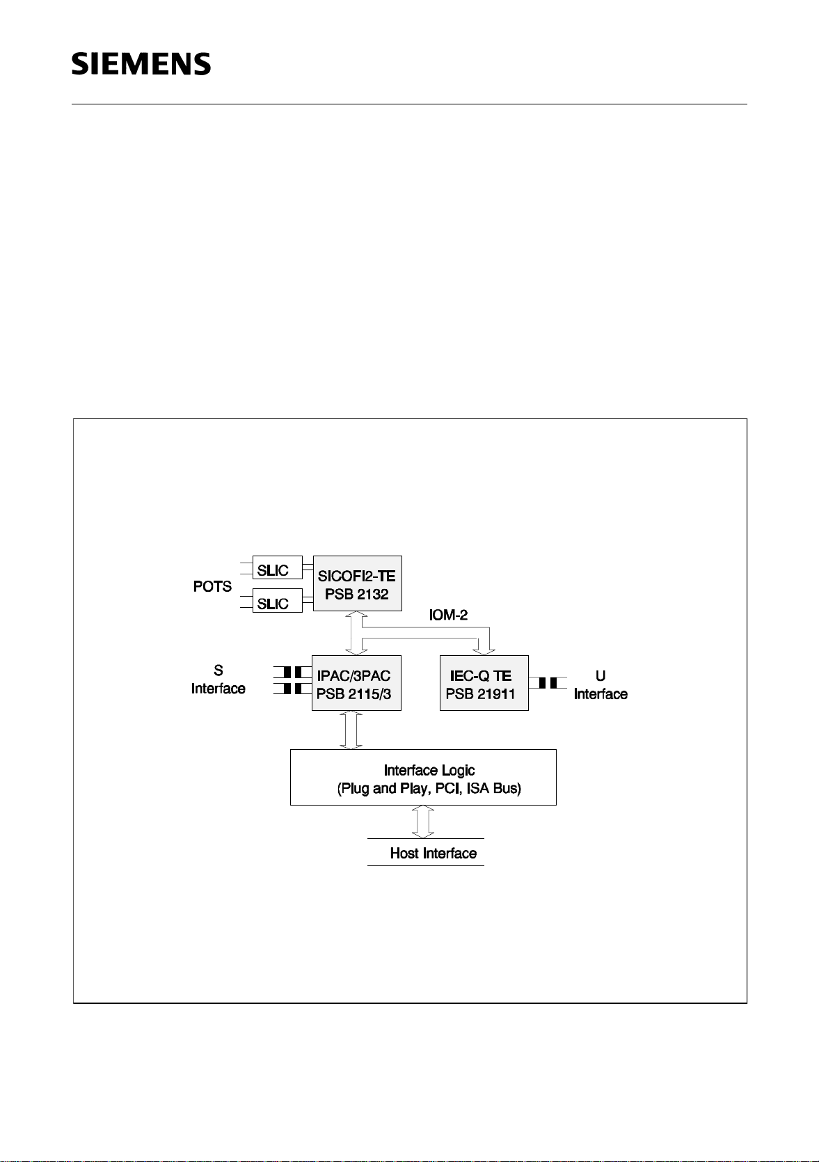
1.7 System Integration
Due to the IOM-2 interface the IEC-Q TE can be combined with a variety of other devices
to fit in numerous applications. This chapter only shows some typical applications of the
IEC-Q TE.
1.7.1 ISDN PC Adapter Card
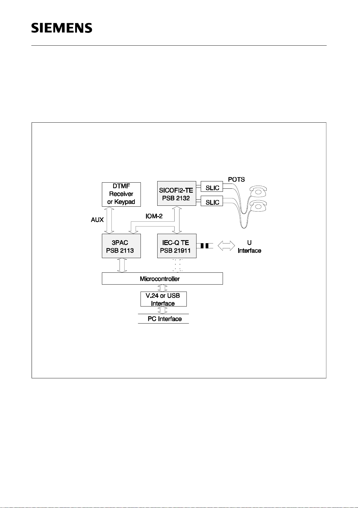
An ISDN adapter card which supports the U-interface may be realized using the
IEC-Q TE together with the PSB 2113 3PAC (
and two B-channel HDLC controllers. Optionally, a PSB 2132 SICOFI2-TE can be
connected to provide two POTS interfaces. If an S-interface is required, the PSB 2115
IPAC can be used instead of the 3PAC.
figure 5
). The 3PAC provides a D-channel
Figure 5 ISDN PC Adapter Card
Semiconductor Group 22 11.97
PSB 21911
PSF 21911
System Integration
1.7.2 ISDN Stand-Alone Terminal with POTS Interface
The IEC-Q TE can be integrated in a microcontroller based stand-alone terminal
(figure 6) that is connected to the communications interface of a PC. The PSB 2132
SICOFI-TE enables connect ion of analog terminals (e.g. telepho nes or fax) to its dual
channel POTS interface.
Figure 6 ISDN Stand-Alone Terminal with POTS Interface
Semiconductor Group 23 11.97
PSB 21911
PSF 21911
System Integration
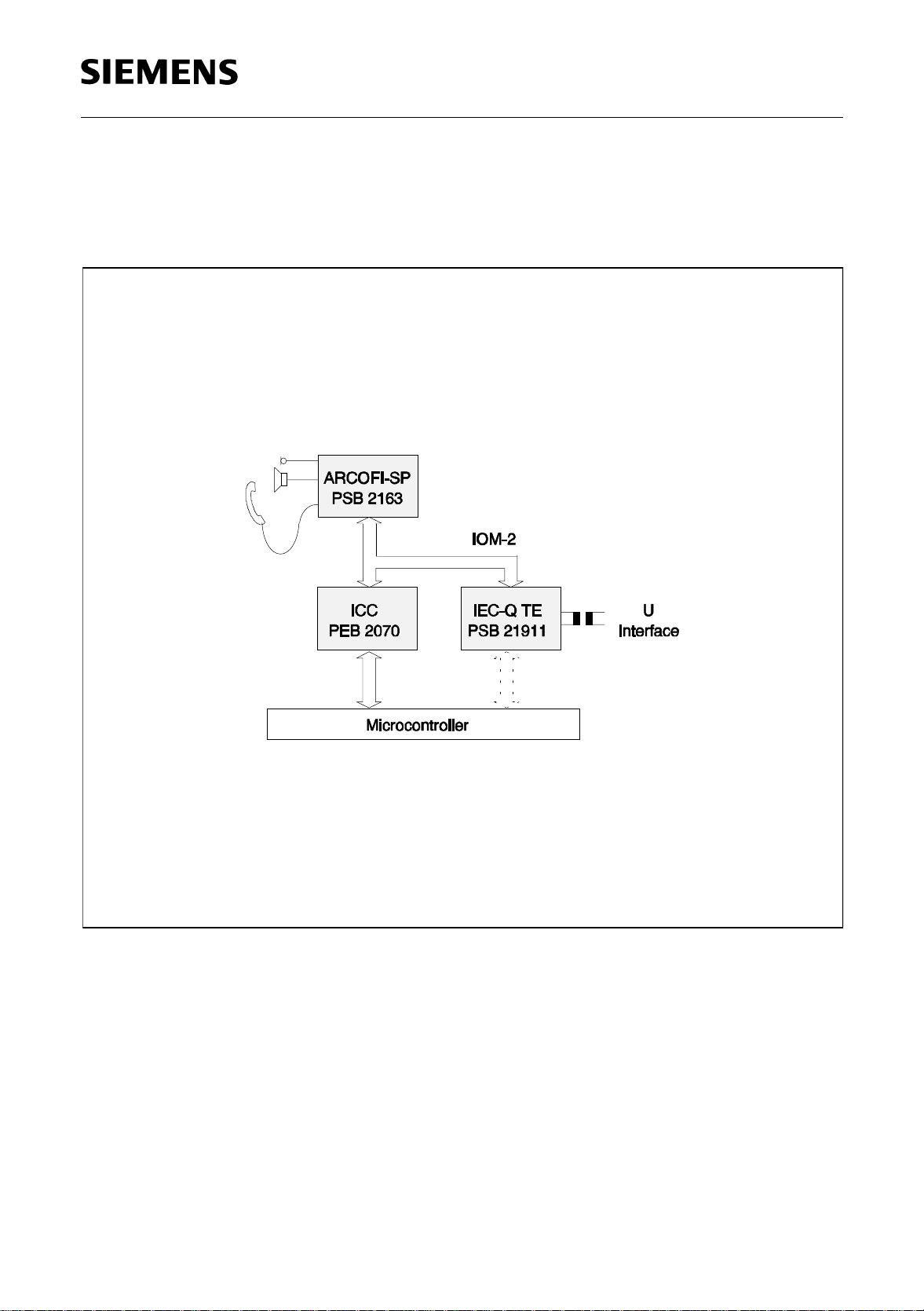
1.7.3 ISDN Feature Phone
An ISDN feature phone with U-interface can be built using the IEC-Q TE together with
the ARCOFI-SP and the ICC.
Figure 7 ISDN Feature Phone
Semiconductor Group 24 11.97
PSB 21911
PSF 21911
System Integration
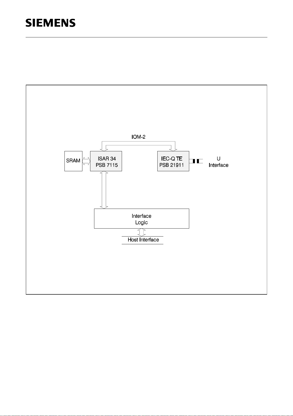
1.7.4 ISDN-Modem PC Card
The combination of the IEC-Q TE and a PSB 7115 I SAR 34 allows to build an ISDNmodem PC card .
Figure 8 ISDN-Modem PC Card
Semiconductor Group 25 11.97
PSB 21911
PSF 21911
Operating Modes
2 Functional Description
2.1 Operating Modes
The default configuration after pow er-on or external reset depends on t he state of the
PMODE pin. The cases µP mode and stand-alone mode have to be distinguished:
µP mode (
PMODE
= VDD)
In µP mode a microprocessor inte rface gives access t o the IOM-2 channel r egi st ers as
well as configuration registers. The operating mode is selected via bits STCR:MS0-MS2
according to
table 2
. The STCR register is described on page 119.
Test modes Send Single Pulses, Quiet Mode or Data Through are invoked via the
corresponding C/I channel command (page 75) or via bits STCR:TM1-2 (
Stand-alone mode (
PMODE
= GND)
table 3
).
In stand-alone mode the operating mode is selected via pin strapping according to
table 2
. It is possible to change the mode of a device during operation (e.g. for test
purposes) if the mode change is followed by a reset.
The test modes Send Single Pulses (SSP), Quiet Mode (QM) and Data Through (DT)
are invoked via the corresponding C/I channel command (page 75) or via pins RES
TSP (
table 3
).
and
Table 2 Modes of Operation (µP and Stand-Alone Mode)
Mode Selection Output Pins U
Synchronized
Mode
NT 0 0 0 512 7680
NT 1 0 0 512 7680
NT-Auto 0 0 1 512 7680
TE 0 1 0 1536 7680
TE 1 1 0 1536 7680
Bit/Pin
MS2
Bit/Pin
MS1
Bit/Pin
MS0
DCL
OUT
CLS
OUT
2)
2)
2)
2)
2)
Superframemarker
no
yes
no
no
yes
1)
reserved others
1)
Notes:
Semiconductor Group 26 11.97
1 DCL-period high-phase of FSC at superframe position
2 DCL-periods high-phase of FSC at normal position
2)
CLS-clock signal not available while device is in power-down
Table 3 Test Modes
PSB 21911
PSF 21911
Operating Modes
Test-Mode
Master-Reset
1)
Send Single-Pulses
Data-Through
3)
2)
Bit TM1/
Pin RES
00
11
01
Bit TM2/
Pin TSP
Normal 1 0
1)
Used for Quiet Mode and Return Loss measurements
2)
Used for Pulse Mask measurements
3)
Used for Insertion Loss, Power Spect ral Density and Tot al Power measurements
Table 4 DOUT Driver Modes
Mode Pin
RES
Pin
1)
TSP
2)
Pin /
Bit
DOD
Pin DOUT Output Driver
Value DOUT in
active time
slot
DOUT in
passive time
slot
Pin-Reset 0 0 x 0 low int. p u ll-up
1 int. pull-up
Normal
(Tristate)
Normal
3)
(Open Drain
1)
In stand-alone mode and µP mode
2)
Only in stand-alone mode. In µP mode the output driver of pin DOUT is selected via bit DOD in the ADF2
regist er
3)
External pull-up resistors required (typ.1 kΩ)
)
1000low high Z
1high
1010low floating
1floating
Semiconductor Group 27 11.97
2.2 Devi ce Arch itecture
In µP mode the following interfaces and functional blocks are used:
• IOM-2 interface see pp. 30
• Microprocessor interface pp. 39, 81, 112
• U-transceiver pp. 40
• Clock G ener ation pp. 111
• Reset pp. 93
• Factory Test Unit
PSB 21911
PSF 21911
Device Architecture
Figure 9 IEC-Q TE Device Architecture (µP Mode)
Semiconductor Group 28 11.97
PSB 21911
PSF 21911
Device Architecture
In stand-alone mode the following interfaces and functional bloc ks are use d:
• Mode Selection see pp. 26
• IOM-2 interface pp. 30
• IOM-2 configuration pp. 36, 38
• U-transceiver pp. 40
• Clock Generation pp. 111
• Reset pp. 93
• Power Controller Interface pp. 94
• Factory Test Unit
Figure 10 IEC-Q TE Device Architecture (Stand-Alone Mode)
Semiconductor Group 29 11.97
PSB 21911
PSF 21911
IOM®-2 Interface
2.3 IOM®-2 Interface
The IOM-2 interface is used to interconnect telecommunication ICs. It provides a
symmetrical full-dupl ex communicat ion link, containing us er dat a, control/program ming
and status channels. The structure used follows the 2B + 1D-channel structure of ISDN.
The ISDN user data rate of 144 kbit/s (B1 + B2 + D) is transmitted in both directions over
the interface.
The IOM-2 interface is a generalization and enhancement of the IOM-1 interface.
®
2.3.1 IOM
The IOM-2 interface comprises two clock lines for synchronization and two data lines.
Data is carried over Data Upstream (DU) and Data Downstream (DD) signals. The
downstream and upstream di rection are always defined with respect to the exchan ge.
Downstream refers to information flow from the exchange to the subscriber and
upstream vice versa respectively. The IOM-2 Interface Specification describes open
drain data lines with external pull-up resistors. However, if operation is logically point-topoint, tristate operation is possible as well.
-2 Frame Structure
The data is clocked by a Data Clock (DCL) that operates at twice the data rate. Frames
are delimited by an 8-kHz Frame Synchronization Clock (FSC). Incoming data is
sampled on every second falling edge of the DCL cl ock.
Figure 11 IOM®-2 Clocks and Data Lines
Within one FSC period 32 bit or 96 bit are transmitted, corresponding to DCL
frequencies of 512 kHz or 1.536 MHz.
Two optimized IOM-2 timing modes exist:
– NT mode for NT1 applications
– TE mode for terminal and intelligent NT applications
Semiconductor Group 30 11.97
 Loading...