

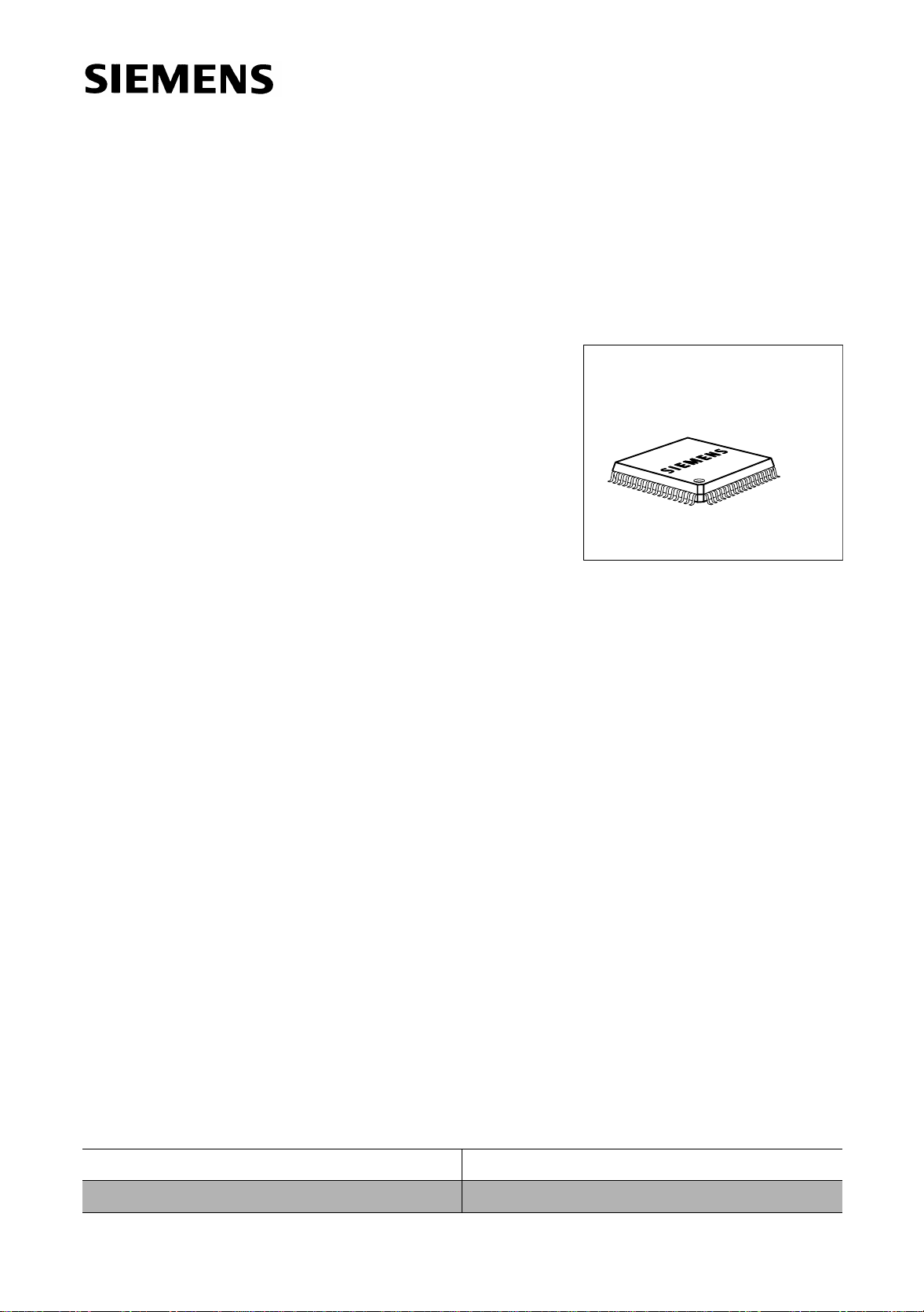
Siemens PSB2168 Datasheet

ICs for Communications
Digital Answering Machine
SAM
PSB 2168 Version 2.1
Data Sheet 11.97
DS 1

PSB 2168
Revision History: Current Version: 11.97
Previous Version: Preliminary Data Sheet 09.97
Page
(in previous
Version)
Page
(in new
Version)
Subjects (major changes since last revision)
Index added
For questions on technology, delivery and prices please contact the Semiconductor
Group Offices in Germany or the Siemens Companies and Representatives worldwide:
see our webpage at http://www.siemens.de/Semiconductor/address/address.htm.
Edition 11.97
Published by Siemens AG,
HL TS,
Balanstraße 73,
81541 München
© Siemens AG 1997.
All Rights Reserved.
Attention please!
As far as patents or other rights of third parties are concerned, liability is only assumed for components, not for
applications, processes and c irc uit s imp lemented within componen ts or as s em blies.
The information describe s the t yp e of co m ponent and shall not be considered as assured characteristics.
Terms of delivery and rights to ch ange design reserved.
Due to technical requireme nt s com ponents may contain dange rous substances. For informatio n on t he t y pes in
question please contact yo ur nearest Siemens Office, Semic onductor Group.
Siemens AG is an approved CECC manufacturer.
Packing
Please use the recycling ope rat ors k now n t o y ou. W e ca n als o help you – get in touch with your neares t sa les
office. By agreement we will take packing material back, if it is sorted. You must bear the costs of transport.
For packing material that is returned to us unsorted or which we are not obliged to accept, we shall have to invoice
you for any costs incurred.
Components used in life-support devices or systems must be expressly authorized for such purpose!
Critical components
systems
1 A critical component is a component used in a life-support device or system whose failure can reasonably be
2 Life support devices or system s are int ended (a) to be implanted in the huma n body, or (b) to support and/or
2
with the express written approv al of the Semiconductor Group of Siem ens AG.
expected to cause the failure of that life-support device or system, or to affect its safety or effectiveness of that
device or system.
maintain and sustain human life. If th ey fail, it is rea so nable to assume that the health of th e us er m ay be endangered.
1
of the Semiconductor Group of Siemens AG, may only be used in life -s upport devices or

PSB 2168
1 Overview . . . . . . . . . . . . . . . . . . . . . . . . . . . . . . . . . . . . . . . . . . . . . . . . .10
1.1 Features . . . . . . . . . . . . . . . . . . . . . . . . . . . . . . . . . . . . . . . . . . . . . . . . . .11
1.2 Pin Configuration . . . . . . . . . . . . . . . . . . . . . . . . . . . . . . . . . . . . . . . . . . . .12
1.3 Pin Definitions and Functions . . . . . . . . . . . . . . . . . . . . . . . . . . . . . . . . . .13
1.4 Logic Symbol . . . . . . . . . . . . . . . . . . . . . . . . . . . . . . . . . . . . . . . . . . . . . . .16
1.5 Functional Block Diagram . . . . . . . . . . . . . . . . . . . . . . . . . . . . . . . . . . . . .17
1.6 System Integration . . . . . . . . . . . . . . . . . . . . . . . . . . . . . . . . . . . . . . . . . .17
1.6.1 Stand-Alone Answering Machine . . . . . . . . . . . . . . . . . . . . . . . . . . . . . . .19
2 Functional Description . . . . . . . . . . . . . . . . . . . . . . . . . . . . . . . . . . . . . .21
2.1 Functional Units . . . . . . . . . . . . . . . . . . . . . . . . . . . . . . . . . . . . . . . . . . . . .24
2.1.1 Line Echo Canceller . . . . . . . . . . . . . . . . . . . . . . . . . . . . . . . . . . . . . . . . .24
2.1.2 DTMF Detector . . . . . . . . . . . . . . . . . . . . . . . . . . . . . . . . . . . . . . . . . . . . .26
2.1.3 CNG Detector . . . . . . . . . . . . . . . . . . . . . . . . . . . . . . . . . . . . . . . . . . . . . .27
2.1.4 Alert Tone Detector . . . . . . . . . . . . . . . . . . . . . . . . . . . . . . . . . . . . . . . . . .28
2.1.5 CPT Detector . . . . . . . . . . . . . . . . . . . . . . . . . . . . . . . . . . . . . . . . . . . . . . .29
2.1.6 Caller ID Decoder . . . . . . . . . . . . . . . . . . . . . . . . . . . . . . . . . . . . . . . . . . .31
2.1.7 DTMF Generator . . . . . . . . . . . . . . . . . . . . . . . . . . . . . . . . . . . . . . . . . . . .33
2.1.8 Speech Coder . . . . . . . . . . . . . . . . . . . . . . . . . . . . . . . . . . . . . . . . . . . . . .34
2.1.9 Speech Decoder . . . . . . . . . . . . . . . . . . . . . . . . . . . . . . . . . . . . . . . . . . . .36
2.1.10 Digital Interface . . . . . . . . . . . . . . . . . . . . . . . . . . . . . . . . . . . . . . . . . . . . .37
2.1.11 Universal Attenuator . . . . . . . . . . . . . . . . . . . . . . . . . . . . . . . . . . . . . . . . .39
2.1.12 Automatic Gain Control Unit . . . . . . . . . . . . . . . . . . . . . . . . . . . . . . . . . . .40
2.1.13 Equalizer . . . . . . . . . . . . . . . . . . . . . . . . . . . . . . . . . . . . . . . . . . . . . . . . . .42
2.2 Memory Management . . . . . . . . . . . . . . . . . . . . . . . . . . . . . . . . . . . . . . . .44
2.2.1 File Definition and Access . . . . . . . . . . . . . . . . . . . . . . . . . . . . . . . . . . . . .45
2.2.2 User Data Word . . . . . . . . . . . . . . . . . . . . . . . . . . . . . . . . . . . . . . . . . . . . .47
2.2.3 High Level Memory Management Commands . . . . . . . . . . . . . . . . . . . . .48
2.2.4 Low Level Memory Management Commands . . . . . . . . . . . . . . . . . . . . . .56
2.2.5 Execution Time . . . . . . . . . . . . . . . . . . . . . . . . . . . . . . . . . . . . . . . . . . . . .58
2.2.6 Special Notes on File Commands . . . . . . . . . . . . . . . . . . . . . . . . . . . . . . .59
2.3 Miscellaneous . . . . . . . . . . . . . . . . . . . . . . . . . . . . . . . . . . . . . . . . . . . . . .60
2.3.1 Real Time Clock . . . . . . . . . . . . . . . . . . . . . . . . . . . . . . . . . . . . . . . . . . . .60
2.3.2 SPS Control Register . . . . . . . . . . . . . . . . . . . . . . . . . . . . . . . . . . . . . . . .60
2.3.3 Reset and Power Down Mode . . . . . . . . . . . . . . . . . . . . . . . . . . . . . . . . . .60
2.3.4 Interrupt . . . . . . . . . . . . . . . . . . . . . . . . . . . . . . . . . . . . . . . . . . . . . . . . . . .61
2.3.5 Abort . . . . . . . . . . . . . . . . . . . . . . . . . . . . . . . . . . . . . . . . . . . . . . . . . . . . .62
2.3.6 Revision Register . . . . . . . . . . . . . . . . . . . . . . . . . . . . . . . . . . . . . . . . . . .63
2.3.7 Hardware Configuration . . . . . . . . . . . . . . . . . . . . . . . . . . . . . . . . . . . . . .63
2.3.8 Auxiliary Clock Generation . . . . . . . . . . . . . . . . . . . . . . . . . . . . . . . . . . . .64
2.3.9 Dependencies of Modules . . . . . . . . . . . . . . . . . . . . . . . . . . . . . . . . . . . . .64
2.4 Interfaces . . . . . . . . . . . . . . . . . . . . . . . . . . . . . . . . . . . . . . . . . . . . . . . . . .66
®
2.4.1 IOM
-2 Interface . . . . . . . . . . . . . . . . . . . . . . . . . . . . . . . . . . . . . . . . . . . .66
Semiconductor Group 3 11.97

PSB 2168
2.4.2 SSDI Interface . . . . . . . . . . . . . . . . . . . . . . . . . . . . . . . . . . . . . . . . . . . . . .70
2.4.3 Serial Control Interface . . . . . . . . . . . . . . . . . . . . . . . . . . . . . . . . . . . . . . .72
2.4.4 Memory Interface . . . . . . . . . . . . . . . . . . . . . . . . . . . . . . . . . . . . . . . . . . . .76
2.4.5 Auxiliary Parallel Port . . . . . . . . . . . . . . . . . . . . . . . . . . . . . . . . . . . . . . . .85
3 Detailed Register Description . . . . . . . . . . . . . . . . . . . . . . . . . . . . . . . .87
3.1 Status Register . . . . . . . . . . . . . . . . . . . . . . . . . . . . . . . . . . . . . . . . . . . . .87
3.2 Hardware Configuration Registers . . . . . . . . . . . . . . . . . . . . . . . . . . . . . .89
3.3 Read/Write Registers . . . . . . . . . . . . . . . . . . . . . . . . . . . . . . . . . . . . . . . .93
3.3.1 Register Table . . . . . . . . . . . . . . . . . . . . . . . . . . . . . . . . . . . . . . . . . . . . . .93
3.3.2 Register Naming Conventions . . . . . . . . . . . . . . . . . . . . . . . . . . . . . . . . . .94
4 Electrical Characteristics . . . . . . . . . . . . . . . . . . . . . . . . . . . . . . . . . . .160
4.1 Absolute Maximum Ratings . . . . . . . . . . . . . . . . . . . . . . . . . . . . . . . . . . .160
4.2 DC Characteristics . . . . . . . . . . . . . . . . . . . . . . . . . . . . . . . . . . . . . . . . . .160
4.3 AC Characteristics . . . . . . . . . . . . . . . . . . . . . . . . . . . . . . . . . . . . . . . . . .162
5 Package Outlines . . . . . . . . . . . . . . . . . . . . . . . . . . . . . . . . . . . . . . . . . .182
IOM®, IOM®-1, IOM®-2, SICOFI®, SICOFI®-2, SICOFI®-4, SICOFI®-4µC, SLICOFI®, ARCOFI
ARCOFI
SICAT
DigiTape
Semiconductor Group 4 11.97
®
-SP, EPIC®-1, EPIC®-S, ELIC®, IPAT®-2, ITAC®, ISAC®-S, ISAC®-S TE, ISAC®-P, ISAC®-P TE, IDEC®,
®
, OCTAT®-P, QUAT®-S are registered trademarks of S iem ens AG.
™
, MUSAC™-A, FALC™54, IWE™, SARE™, UTPT™, ASM™, ASP™ are trademarks of Siemens AG.
®
, ARCOFI®-BA,

PSB 2168
List of Figures Page
General
Figure 1: Pin Configuration of PSB 2168. . . . . . . . . . . . . . . . . . . . . . . . . . . . . . . . . 12
Figure 2: Logic Symbol of PSB 2168. . . . . . . . . . . . . . . . . . . . . . . . . . . . . . . . . . . . 16
Figure 3: Block Diagram of PSB 2168. . . . . . . . . . . . . . . . . . . . . . . . . . . . . . . . . . . 17
Figure 4: Featurephone with Answering Machine for ISDN Terminal . . . . . . . . . . . 18
Figure 5: Stand-Alone Answering Machine with ARAM/EPROM . . . . . . . . . . . . . . 19
Figure 6: Stand-Alone Answering Machine with Flash Memory . . . . . . . . . . . . . . . 20
Functional Units
Figure 7: Functional Units - Overview . . . . . . . . . . . . . . . . . . . . . . . . . . . . . . . . . . . 21
Figure 8: Functional Units - Recording a Phone Conversation . . . . . . . . . . . . . . . . 23
Figure 9: Line Echo Cancellation Unit - Block Diagram. . . . . . . . . . . . . . . . . . . . . . 24
Figure 10: DTMF Detector - Block Diagram . . . . . . . . . . . . . . . . . . . . . . . . . . . . . . . 26
Figure 11: CNG Detector - Block Diagram . . . . . . . . . . . . . . . . . . . . . . . . . . . . . . . . 27
Figure 12: Alert Tone Detector - Block Diagram . . . . . . . . . . . . . . . . . . . . . . . . . . . . 28
Figure 13: CPT Detector - Block Diagram . . . . . . . . . . . . . . . . . . . . . . . . . . . . . . . . . 29
Figure 14: CPT Detector - Cooked Mode . . . . . . . . . . . . . . . . . . . . . . . . . . . . . . . . . 29
Figure 15: Caller ID Decoder - Block Diagram . . . . . . . . . . . . . . . . . . . . . . . . . . . . . 31
Figure 16: DTMF Generator - Block Diagram . . . . . . . . . . . . . . . . . . . . . . . . . . . . . . 33
Figure 17: Speech Coder - Block Diagram . . . . . . . . . . . . . . . . . . . . . . . . . . . . . . . . 34
Figure 18: Speech Decoder - Block Diagram . . . . . . . . . . . . . . . . . . . . . . . . . . . . . . 36
Figure 19: Digital Interface - Block Diagram . . . . . . . . . . . . . . . . . . . . . . . . . . . . . . . 37
Figure 20: Universal Attenuator - Block Diagram . . . . . . . . . . . . . . . . . . . . . . . . . . . 39
Figure 21: Automatic Gain Control Unit - Block Diagram . . . . . . . . . . . . . . . . . . . . . 40
Figure 22: Automatic Gain Control Unit - Steady State Characteristic . . . . . . . . . . . 40
Figure 23: Equalizer - Block Diagram . . . . . . . . . . . . . . . . . . . . . . . . . . . . . . . . . . . . 42
Memory Management
Figure 24: Memory Management - Data Flow. . . . . . . . . . . . . . . . . . . . . . . . . . . . . . 44
Figure 25: Memory Management - Directory Structure . . . . . . . . . . . . . . . . . . . . . . . 44
Figure 26: Audio File Organization - Example. . . . . . . . . . . . . . . . . . . . . . . . . . . . . . 45
Figure 27: Binary File Organization - Example . . . . . . . . . . . . . . . . . . . . . . . . . . . . . 45
Figure 28: Phrase File Organization - Example. . . . . . . . . . . . . . . . . . . . . . . . . . . . . 46
Miscellaneous
Figure 29: Operation Modes - State Chart. . . . . . . . . . . . . . . . . . . . . . . . . . . . . . . . . 61
Interfaces
®-2
Figure 30: IOM
Figure 31: IOM
Figure 32: IOM
Figure 33: IOM
Interface - Frame Structure . . . . . . . . . . . . . . . . . . . . . . . . . . . . . 66
®
-2 Interface - Frame Start. . . . . . . . . . . . . . . . . . . . . . . . . . . . . . . . . 67
®
-2 Interface - Single Clock Mode . . . . . . . . . . . . . . . . . . . . . . . . . . . 67
®
-2 Interface - Double Clock Mode . . . . . . . . . . . . . . . . . . . . . . . . . . 68
Figure 34: SSDI Interface - Transmitter Timing. . . . . . . . . . . . . . . . . . . . . . . . . . . . . 70
Semiconductor Group 5 11.97

PSB 2168
List of Figures Page
Figure 35: SSDI Interface - Active Pulse Selection . . . . . . . . . . . . . . . . . . . . . . . . . . 71
Figure 36: SSDI Interface - Receiver Timing. . . . . . . . . . . . . . . . . . . . . . . . . . . . . . . 71
Figure 37: Status Register Read Access. . . . . . . . . . . . . . . . . . . . . . . . . . . . . . . . . . 72
Figure 38: Data Read Access . . . . . . . . . . . . . . . . . . . . . . . . . . . . . . . . . . . . . . . . . . 73
Figure 39: Register Write Access . . . . . . . . . . . . . . . . . . . . . . . . . . . . . . . . . . . . . . . 73
Figure 40: Configuration Register Read Access . . . . . . . . . . . . . . . . . . . . . . . . . . . . 74
Figure 41: Configuration Register Write Access or Register Read Command . . . . . 74
Figure 42: ARAM/DRAM Interface - Connection Diagram. . . . . . . . . . . . . . . . . . . . . 77
Figure 43: ARAM/DRAM Interface - Read Cycle Timing. . . . . . . . . . . . . . . . . . . . . . 78
Figure 44: ARAM/DRAM Interface - Write Cycle Timing . . . . . . . . . . . . . . . . . . . . . . 79
Figure 45: ARAM/DRAM Interface - Refresh Cycle Timing. . . . . . . . . . . . . . . . . . . . 79
Figure 46: EPROM Interface - Connection Diagram . . . . . . . . . . . . . . . . . . . . . . . . . 80
Figure 47: EPROM Interface - Read Cycle Timing . . . . . . . . . . . . . . . . . . . . . . . . . . 80
Figure 48: Flash Memory Interface - Connection Diagram . . . . . . . . . . . . . . . . . . . . 81
Figure 49: Flash Memory Interface - Multiple Devices . . . . . . . . . . . . . . . . . . . . . . . 82
Figure 50: Flash Memory Interface - Command Write. . . . . . . . . . . . . . . . . . . . . . . . 83
Figure 51: Flash Memory Interface - Address Write . . . . . . . . . . . . . . . . . . . . . . . . . 83
Figure 52: Flash Memory Interface - Data Write . . . . . . . . . . . . . . . . . . . . . . . . . . . . 84
Figure 53: Flash Memory Interface - Data Read . . . . . . . . . . . . . . . . . . . . . . . . . . . . 84
Figure 54: Auxiliary Parallel Port - Multiplex Mode . . . . . . . . . . . . . . . . . . . . . . . . . . 86
Electrical Characteristics
Figure 55: Input/Output Waveforms for AC-Tests . . . . . . . . . . . . . . . . . . . . . . . . . . 162
Timing Diagrams
Figure 56: Oscillator Circuits . . . . . . . . . . . . . . . . . . . . . . . . . . . . . . . . . . . . . . . . . . 166
®
Figure 57: SSDI/IOM
Figure 58: SSDI/IOM
-2 Interface - Bit Synchronization Timing . . . . . . . . . . . . . . . 167
®
-2 Interface - Frame Synchronization Timing . . . . . . . . . . . . 167
Figure 59: SSDI Interface - Strobe Timing. . . . . . . . . . . . . . . . . . . . . . . . . . . . . . . . 169
Figure 60: Serial Control Interface. . . . . . . . . . . . . . . . . . . . . . . . . . . . . . . . . . . . . . 170
Figure 61: Clock Master Timing. . . . . . . . . . . . . . . . . . . . . . . . . . . . . . . . . . . . . . . . 171
Figure 62: Memory Interface - DRAM Read Access . . . . . . . . . . . . . . . . . . . . . . . . 172
Figure 63: Memory Interface - DRAM Write Access . . . . . . . . . . . . . . . . . . . . . . . . 173
Figure 64: Memory Interface - DRAM Refresh Cycle . . . . . . . . . . . . . . . . . . . . . . . 174
Figure 65: Memory Interface - EPROM Read . . . . . . . . . . . . . . . . . . . . . . . . . . . . . 175
Figure 66: Memory Interface - Samsung Command Write . . . . . . . . . . . . . . . . . . . 176
Figure 67: Memory Interface - Samsung Address Write . . . . . . . . . . . . . . . . . . . . . 177
Figure 68: Memory Interface - Samsung Data Write . . . . . . . . . . . . . . . . . . . . . . . . 178
Figure 69: Memory Interface - Samsung Data Read. . . . . . . . . . . . . . . . . . . . . . . . 179
Figure 70: Auxiliary Parallel Port - Multiplex Mode . . . . . . . . . . . . . . . . . . . . . . . . . 180
Figure 71: Reset Timing . . . . . . . . . . . . . . . . . . . . . . . . . . . . . . . . . . . . . . . . . . . . . 181
Semiconductor Group 6 11.97

PSB 2168
List of Tables Page
General
Table 1: Pin Definitions and Functions. . . . . . . . . . . . . . . . . . . . . . . . . . . . . . . . . . .13
Functional Units
Table 2: Signal Summary . . . . . . . . . . . . . . . . . . . . . . . . . . . . . . . . . . . . . . . . . . . . .22
Table 3: Line Echo Cancellation Unit Registers. . . . . . . . . . . . . . . . . . . . . . . . . . . .25
Table 4: DTMF Detector Control Register . . . . . . . . . . . . . . . . . . . . . . . . . . . . . . . .26
Table 5: DTMF Detector Results . . . . . . . . . . . . . . . . . . . . . . . . . . . . . . . . . . . . . . .26
Table 6: DTMF Detector Parameters . . . . . . . . . . . . . . . . . . . . . . . . . . . . . . . . . . . .26
Table 7: CNG Detector Registers. . . . . . . . . . . . . . . . . . . . . . . . . . . . . . . . . . . . . . .27
Table 8: CNG Detector Result . . . . . . . . . . . . . . . . . . . . . . . . . . . . . . . . . . . . . . . . .27
Table 9: Alert Tone Detector Registers . . . . . . . . . . . . . . . . . . . . . . . . . . . . . . . . . .28
Table 10: Alert Tone Detector Results . . . . . . . . . . . . . . . . . . . . . . . . . . . . . . . . . . . .28
Table 11: CPT Detector Result. . . . . . . . . . . . . . . . . . . . . . . . . . . . . . . . . . . . . . . . . .30
Table 12: CPT Detector Registers . . . . . . . . . . . . . . . . . . . . . . . . . . . . . . . . . . . . . . .30
Table 13: Caller ID Decoder Modes . . . . . . . . . . . . . . . . . . . . . . . . . . . . . . . . . . . . . .31
Table 14: Caller ID Decoder Status . . . . . . . . . . . . . . . . . . . . . . . . . . . . . . . . . . . . . .31
Table 15: Caller ID Decoder Registers. . . . . . . . . . . . . . . . . . . . . . . . . . . . . . . . . . . .31
Table 16: DTMF Generator Registers . . . . . . . . . . . . . . . . . . . . . . . . . . . . . . . . . . . .33
Table 17: Speech Coder Status . . . . . . . . . . . . . . . . . . . . . . . . . . . . . . . . . . . . . . . . .34
Table 18: Speech Coder Registers . . . . . . . . . . . . . . . . . . . . . . . . . . . . . . . . . . . . . .35
Table 19: Speech Decoder Registers. . . . . . . . . . . . . . . . . . . . . . . . . . . . . . . . . . . . .36
Table 20: Digital Interface Registers . . . . . . . . . . . . . . . . . . . . . . . . . . . . . . . . . . . . .37
Table 21: Universal Attenuator Registers. . . . . . . . . . . . . . . . . . . . . . . . . . . . . . . . . .39
Table 22: Automatic Gain Control Registers . . . . . . . . . . . . . . . . . . . . . . . . . . . . . . .41
Table 23: Equalizer Registers . . . . . . . . . . . . . . . . . . . . . . . . . . . . . . . . . . . . . . . . . .42
Memory Management - General
Table 24: Memory Management Registers . . . . . . . . . . . . . . . . . . . . . . . . . . . . . . . .46
Table 25: Memory Management Status . . . . . . . . . . . . . . . . . . . . . . . . . . . . . . . . . . .46
Table 26: Memory Management Parameters. . . . . . . . . . . . . . . . . . . . . . . . . . . . . . .47
Memory Management - Commands
Table 27: Initialize Memory Parameters. . . . . . . . . . . . . . . . . . . . . . . . . . . . . . . . . . .48
Table 28: Initialize Memory Results . . . . . . . . . . . . . . . . . . . . . . . . . . . . . . . . . . . . . .48
Table 29: Activate Memory Parameters . . . . . . . . . . . . . . . . . . . . . . . . . . . . . . . . . . .49
Table 30: Activate Memory Results . . . . . . . . . . . . . . . . . . . . . . . . . . . . . . . . . . . . . .49
Table 31: Activate Memory Result Interpretation . . . . . . . . . . . . . . . . . . . . . . . . . . . .49
Table 32: Open File Parameters . . . . . . . . . . . . . . . . . . . . . . . . . . . . . . . . . . . . . . . .50
Table 33: Open Next Free File Parameters . . . . . . . . . . . . . . . . . . . . . . . . . . . . . . . .50
Table 34: Open Next Free File Results . . . . . . . . . . . . . . . . . . . . . . . . . . . . . . . . . . .51
Table 35: Seek Parameters . . . . . . . . . . . . . . . . . . . . . . . . . . . . . . . . . . . . . . . . . . . .51
Table 36: Cut File Parameters . . . . . . . . . . . . . . . . . . . . . . . . . . . . . . . . . . . . . . . . . .52
Semiconductor Group 7 11.97

PSB 2168
Table 37: Compress File Parameters. . . . . . . . . . . . . . . . . . . . . . . . . . . . . . . . . . . . .52
Table 38: Memory Status Parameters . . . . . . . . . . . . . . . . . . . . . . . . . . . . . . . . . . . .53
Table 39: Memory Status Results . . . . . . . . . . . . . . . . . . . . . . . . . . . . . . . . . . . . . . .53
Table 40: Garbage Collection Parameters . . . . . . . . . . . . . . . . . . . . . . . . . . . . . . . . .53
Table 41: Access File Descriptor Parameters . . . . . . . . . . . . . . . . . . . . . . . . . . . . . .54
Table 42: Access File Descriptor Results. . . . . . . . . . . . . . . . . . . . . . . . . . . . . . . . . .54
Table 43: Read Data Parameters. . . . . . . . . . . . . . . . . . . . . . . . . . . . . . . . . . . . . . . .54
Table 44: Read Data Results . . . . . . . . . . . . . . . . . . . . . . . . . . . . . . . . . . . . . . . . . . .54
Table 45: Write Data Parameters. . . . . . . . . . . . . . . . . . . . . . . . . . . . . . . . . . . . . . . .55
Table 46: Set Address Parameters . . . . . . . . . . . . . . . . . . . . . . . . . . . . . . . . . . . . . .56
Table 47: DMA Read Parameters . . . . . . . . . . . . . . . . . . . . . . . . . . . . . . . . . . . . . . .56
Table 48: DMA Read Results. . . . . . . . . . . . . . . . . . . . . . . . . . . . . . . . . . . . . . . . . . .56
Table 49: DMA Write Parameters. . . . . . . . . . . . . . . . . . . . . . . . . . . . . . . . . . . . . . . .57
Table 50: Block Erase Parameters. . . . . . . . . . . . . . . . . . . . . . . . . . . . . . . . . . . . . . .57
Table 51: Execution Times. . . . . . . . . . . . . . . . . . . . . . . . . . . . . . . . . . . . . . . . . . . . .58
Miscellaneous
Table 52: Real Time Clock Registers. . . . . . . . . . . . . . . . . . . . . . . . . . . . . . . . . . . . .60
Table 53: SPS Registers . . . . . . . . . . . . . . . . . . . . . . . . . . . . . . . . . . . . . . . . . . . . . .60
Table 54: Power Down Bit . . . . . . . . . . . . . . . . . . . . . . . . . . . . . . . . . . . . . . . . . . . . .61
Table 55: Interrupt Source Summary . . . . . . . . . . . . . . . . . . . . . . . . . . . . . . . . . . . . .62
Table 56: Hardware Configuration Checklist . . . . . . . . . . . . . . . . . . . . . . . . . . . . . . .63
Table 57: Auxiliary Clock Generation . . . . . . . . . . . . . . . . . . . . . . . . . . . . . . . . . . . . .64
Table 58: Dependencies of Modules . . . . . . . . . . . . . . . . . . . . . . . . . . . . . . . . . . . . .64
Table 59: File Command Classes . . . . . . . . . . . . . . . . . . . . . . . . . . . . . . . . . . . . . . .65
Interfaces
®
Table 60: SSDI vs. IOM
®
Table 61: IOM
-2 Interface Registers. . . . . . . . . . . . . . . . . . . . . . . . . . . . . . . . . . . . .68
-2 Interface . . . . . . . . . . . . . . . . . . . . . . . . . . . . . . . . . . . . .66
Table 62: SSDI Interface Register . . . . . . . . . . . . . . . . . . . . . . . . . . . . . . . . . . . . . . .71
Table 63: Command Words for Register Access . . . . . . . . . . . . . . . . . . . . . . . . . . . .75
Table 64: Address Field W for Configuration Register Write . . . . . . . . . . . . . . . . . . .75
Table 65: Address Field R for Configuration Register Read . . . . . . . . . . . . . . . . . . .75
Table 66: Supported Memory Configurations. . . . . . . . . . . . . . . . . . . . . . . . . . . . . . .76
Table 67: Address Line Usage (ARAM/DRAM Mode) . . . . . . . . . . . . . . . . . . . . . . . .78
Table 68: Refresh Frequency Selection . . . . . . . . . . . . . . . . . . . . . . . . . . . . . . . . . . .79
Table 69: Address Line Usage (Samsung Mode). . . . . . . . . . . . . . . . . . . . . . . . . . . .81
Table 70: Flash Memory Command Summary. . . . . . . . . . . . . . . . . . . . . . . . . . . . . .82
Table 71: Static Mode Registers . . . . . . . . . . . . . . . . . . . . . . . . . . . . . . . . . . . . . . . .85
Table 72: Multiplex Mode Registers . . . . . . . . . . . . . . . . . . . . . . . . . . . . . . . . . . . . . .85
Table 73: Signal Encoding . . . . . . . . . . . . . . . . . . . . . . . . . . . . . . . . . . . . . . . . . . . . .95
Semiconductor Group 8 11.97

PSB 2168
Electrical Characteristics
Table 74: Status Register Update Timing . . . . . . . . . . . . . . . . . . . . . . . . . . . . . . . .165
Semiconductor Group 9 11.97

PSB 2168
Overview
1Overview
General
General
The PSB 2168 provides a solution for an embedded answering in an IOM®-2 based
system.
™
The chip features recording by DigiTape
™
Messages recorded with DigiTape
can be played back with variable speed without
pitch alteration. Messages recorded with a higher bitrate can be converted into
messages with a lower b itrate arbitrarily. Current m embers of DigiTape (TM) span the
range from 3.3 kbit/s to 10.3 kbit/s.
Furthermore the PSB 2168, V2.1 has a a caller ID decoder, DTMF recognition and
generation and call progress tone detection. The frequency response of cheap
microphones or loudspeakers can be corrected by a programmable equalizer.
Messages and user da ta can be stored in AR AM/ DRA M or flas h memory which can be
directly connected to the PSB 2168. The PSB 2168 also supports a voice prompt
EPROM for fixed announcements.
®
The PSB 2168 provides an IOM
-2 compatible inte rface with t wo channels f or speech
data.
®
Alternatively to the IOM
-2 compatible interface the PSB 2 168 su pport s a si mple se rial
data interface (SSDI) with separate strobe sign als for each direction (linear PCM data,
one channel).
, a family of high performance algorithms.
The chip is programmed by a simple four wire serial control interface and can inform the
microcontroller of new events by an interrupt sign al. For data retention the PSB 2168
supports a power down mode where only the real time clock and the memory refresh (in
case of ARAM/DRAM) are operational.
The PSB 2168 supports interface pins to +5 V levels.
Semiconductor Group 10 11.97
Digital Answering Machine
PSB 2168
SAM
Version 2.1 CMOS
1.1 Features
Digital Functions
• High performance recording by DigiTape
• Selectable compression rate (3.3 kbit/s, 10.3 kbit/s)
• Variable playback speed
• Support for ARAM or Flash Memory
• Optional voice prompt EPROM
• DTMF generation and detection
• Call progress tone detection
• Caller ID recognition
• Direct memory access
• Real time clock
• Equalizer
• Automatic gain control
• Automatic timestamp
• Auxiliary parallel port
• Ultra low power refresh mode
™
P-MQFP-80
General Features
®
• SSDI/IOM
-2 compatible interface
• Serial control interface for programming
• Master clock generation for common codecs
Type Package
PSB 2168 P-MQFP-80
Semiconductor Group 11 11.97
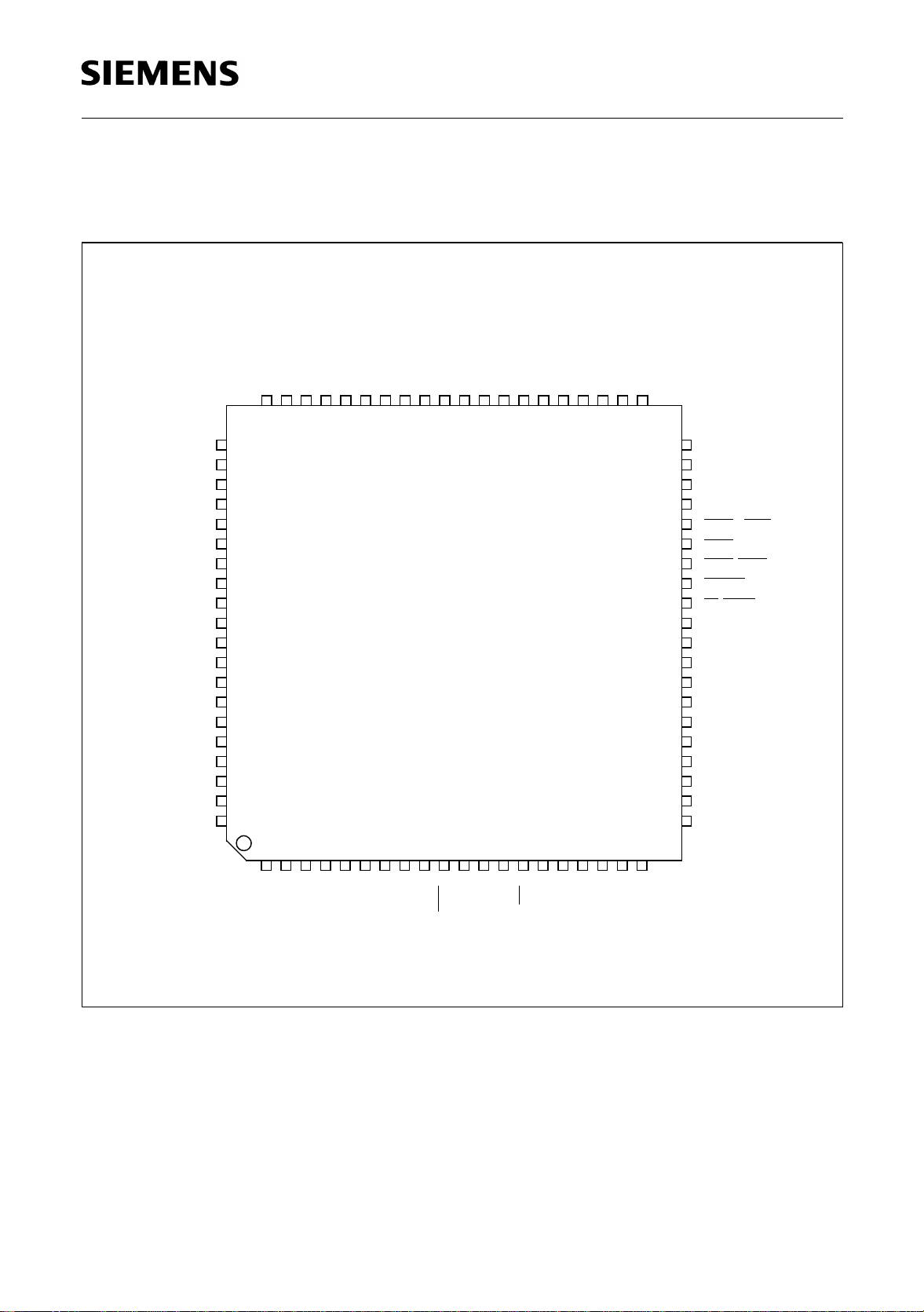
1.2 Pin Configuration
(top view)
PSB 2168
Overview
V
MA
MA
MA
MA
V
MA
MA
MA
MA
V
MA
MA
MA
MA
RST
V
DD
V
SS
DD
V
SS
DD
V
SS
DDP
1MD2
3
MD
MD0V
DDP
VSSV
SS
VDDV
SS
MA3MA2MA1MA0MD7MD
RO
6
SS
MD5MD4MD
VDDV
4160 50
V
61
4
5
6
7
40
SS
V
DD
SPS
1
SPS
0
CAS1/FCS
CAS0/ALE
/FOE
RAS
VPRD
W
/FWE
FRDY
V
SS
V
DD
/FCLE
8
9
10
70
11
SAM
30
PSB 2168
DRST
12
13
14
15
DXST
DD/DR
DU/DX
DCL
FSC
V
SS
V
80
21
DD
110 20
DDA
V
XTAL1XTAL
2
SSA
V
OSC1OSC
2
V
DD
SS
V
INT
CLK
SDR
SDX
SCLK
CS
V
DD
SS
V
AFEFS
RO
SS
V
AFECLK
Figure 1 Pin Configuration of PSB 2168
Semiconductor Group 12 11.97

1.3 Pin Definitions and Functions
Table 1 Pin Definitions and Functions
PSB 2168
Overview
Pin No.
P-MQFP-80
41, 80
Symbol Dir. Reset Function
V
DDP
-- Power supply (5V %)
10±
Power supply for the interface.
7, 15, 21,
29, 39, 49,
V
DD
-- Power supply (3.0 V - 3.6 V)
Power supply for logic.
58, 61, 67,
73
1
V
DDA
-- Power supply (3.0 V - 3.6 V)
Power supply for clock generator.
4
V
SSA
-- Power supply (0 V)
Ground for clock generator.
9, 16,20,
22, 30, 40,
V
SS
-- Power supply (0 V)
Ground for logic and interface.
48, 57, 59,
60, 78, 66,
72
17 AFEFS O L Analog Frontend Frame Sync:
8 kHz frame synchronization signal for the
analog front end.
18 AFECLK O L Analog Frontend Clock:
Clock signal for the analog front end.
79 RST I - Reset:
Active high reset signal.
23 FSC I - Data Frame Synchronization:
®
8 kHz frame synchronization signal (IOM
-2 and
SSDI mode).
24 DCL I - Data Clock:
Data Clock of the serial data interface.
®
26 DD/DR I/ODI- IOM
Receive data from IOM
-2 Compatible Mode:
®
-2 controlling device.
SSDI Mode:
Receive data of the strobed serial data interface.
Semiconductor Group 13 11.97
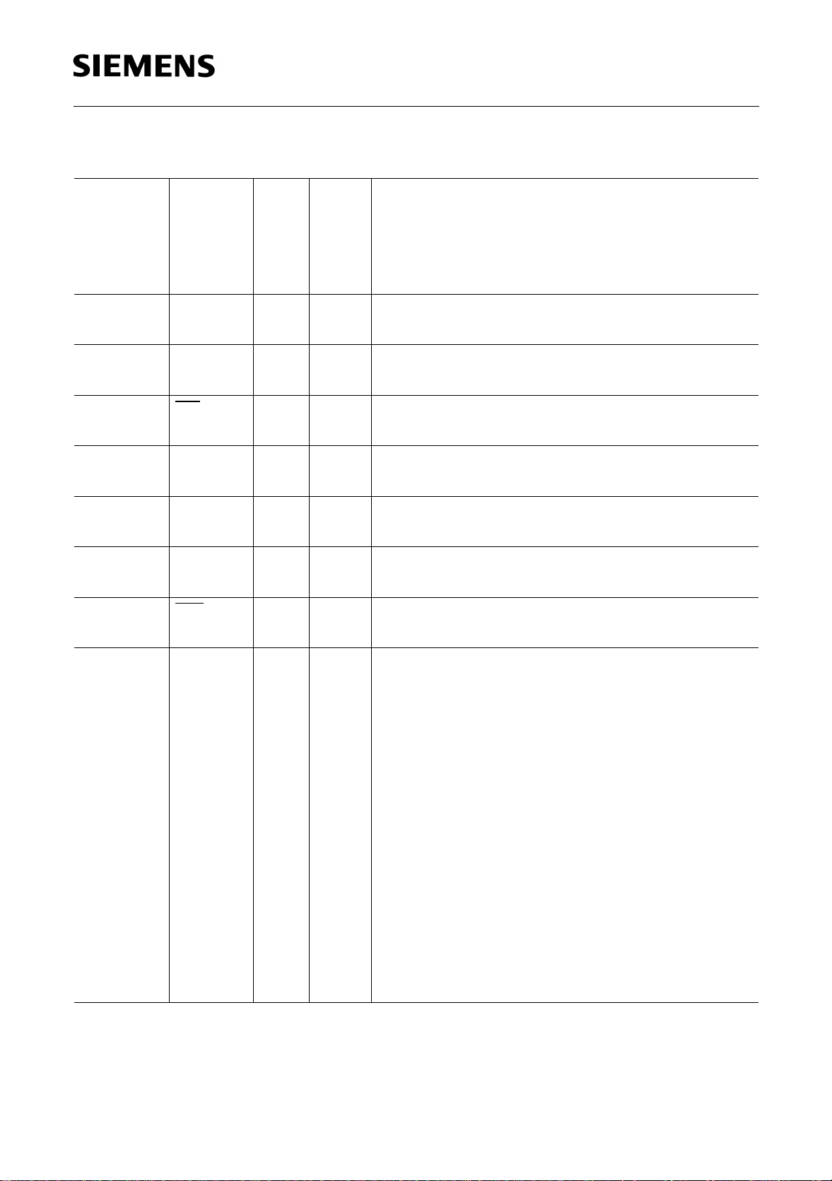
Table 1 Pin Definitions and Functions
PSB 2168
Overview
25 DU/DX I/OD
- IOM®-2 Compatible Mode:
Transmit data to IOM
O/
OD
SSDI Mode:
Transmit data of the strobed serial data
interface.
27 DXST O L DX Strobe:
Strobe for DX in SSDI interface mode.
28 DRST I - DR Strobe:
Strobe for DR in SSDI interface mode.
14 CS
I- Chip Select:
Select signal of the serial control interface (SCI).
11 SCLK I - Serial Clock:
Clock signal of the serial control interface (SCI).
13 SDR I - Serial Data Receive:
Data input of the serial control interface (SCI).
12 SDX O/
OD
H Serial Data Transmit:
Data Output of the serial control interface (SCI).
®
-2 controlling device.
10 INT
52
53
54
55
62
63
64
65
68
69
70
71
74
75
76
77
MA
MA
MA
MA
MA
MA
MA
MA
MA
MA
MA
MA
MA
MA
MA
MA
0
1
2
3
4
5
6
7
8
9
10
11
12
13
14
15
O/
OD
I/O
I/O
I/O
I/O
I/O
I/O
I/O
I/O
I/O
I/O
I/O
I/O
I/O
I/O
I/O
I/O
H Interrupt
New status available.
1)
L
L
L
L
L
L
L
Memory Address 0-15:
Multiplexed address outputs for ARAM, DRAM
access.
Non-multiplexed address outputs for voice
prompt EPROM.
Auxiliary Parallel Port:
General purpose I/O.
L
L
L
L
L
L
L
L
L
Semiconductor Group 14 11.97
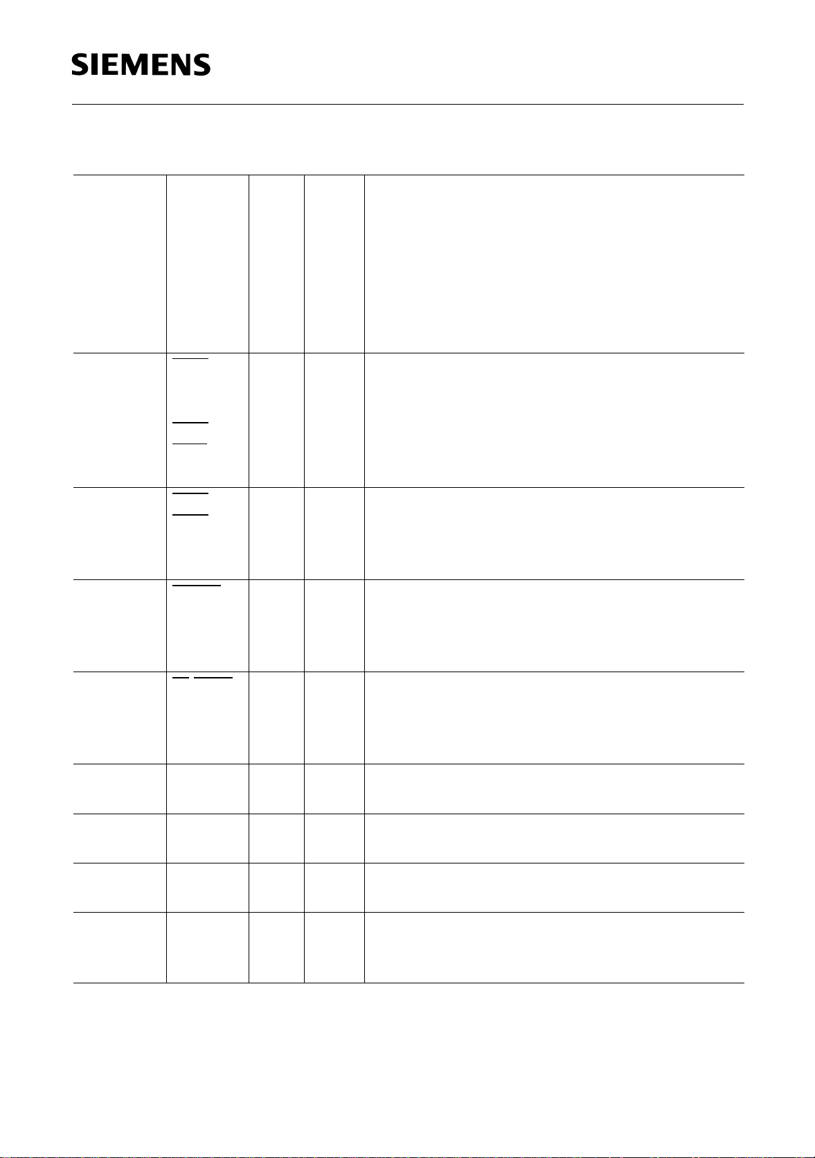
Table 1 Pin Definitions and Functions
PSB 2168
Overview
42
43
44
45
46
47
50
51
35
MD
MD
MD
MD
MD
MD
MD
MD
CAS
ALE
36
CAS
FCS
34 RAS
FOE
0
1
2
3
4
5
6
7
0
I/O
I/O
I/O
I/O
I/O
I/O
I/O
I/O
/
O
-
-
-
-
-
-
-
-
H
Memory Data 0-7:
Memory (ARAM, DRAM, Flash Memory,
EPROM) data bus.
2)
ARAM, DRAM:
Column address strobe for memory bank 0 or 1.
/
1
O
Flash Memory:
Address Latch Enable for address lines A
16-A23
.
Chip select signal for Flash Memory
/
OH2)ARAM, DRAM:
Row address strobe for both memory banks.
Flash Memory:
Output enable signal for Flash Memory.
/
33 VPRD
FCLE
OH2)ARAM, DRAM:
Read signal for voice prompt EPROM.
Flash Memory:
Command latch enable for Flash Memory.
32 W
/FWE OH2)ARAM, DRAM:
Write signal for all memory banks.
Flash Memory:
Write signal for Flash Memory.
31 FRDY I - Flash Memory Ready
Input for Ready/Busy signal of Flash Memory
5
6
OSC
OSC
1
2
I
O
-
Z
Auxiliary Oscillator:
Oscillator loop for 32.768 kHz crystal.
8CLKI-Alternative AFECLK Source
13,824 MHz
2
3
XTAL
XTAL
I
1
O
2
-
Z
Oscillator:
XTAL
XTAL
: External clock or input of oscillator loop.
1
: output of oscillator loop for crystal.
2
Semiconductor Group 15 11.97
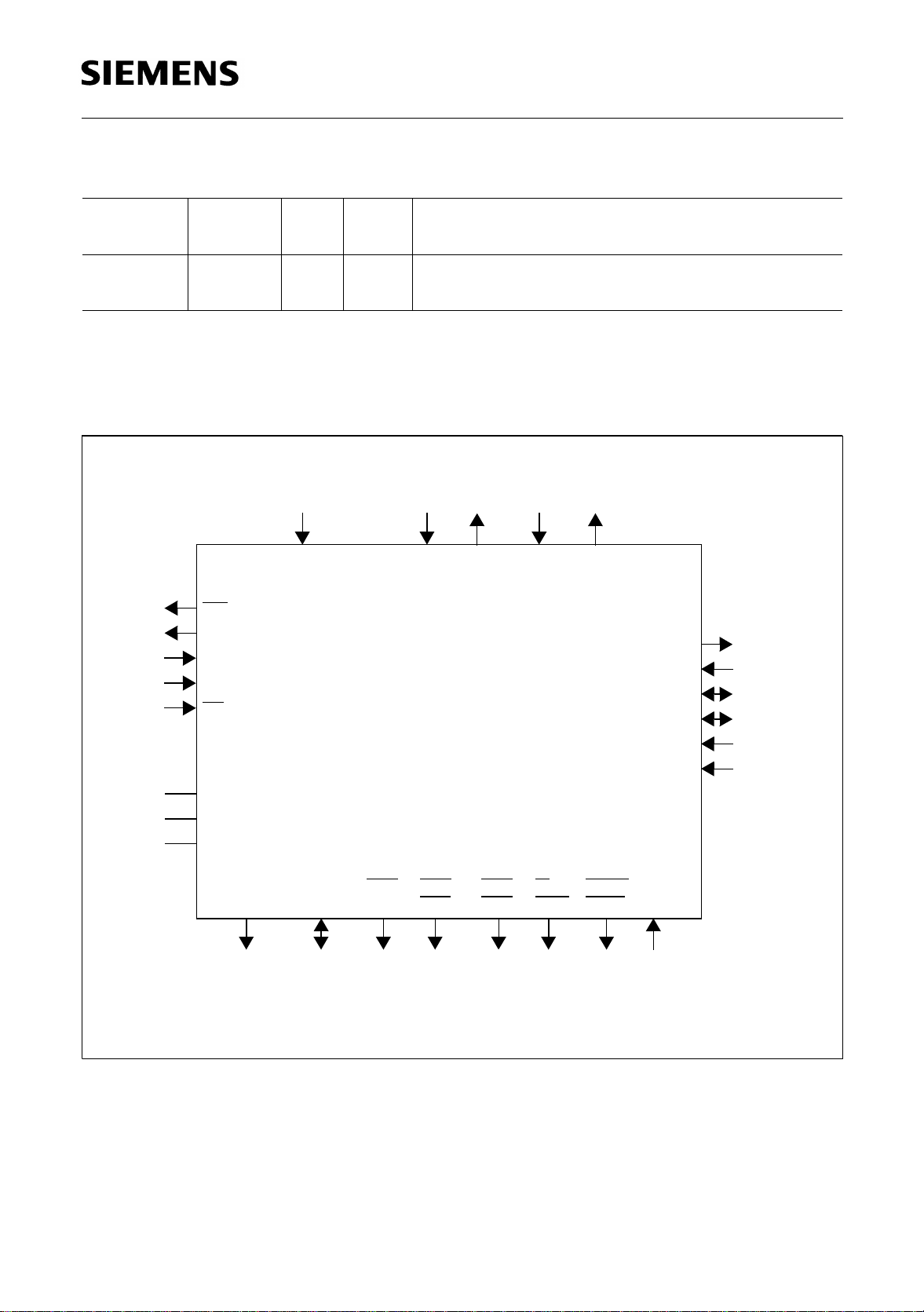
Table 1 Pin Definitions and Functions
PSB 2168
Overview
37
38
SPS
SPS
0
1
O
O
L
L
Multipurpose Outputs:
General purpose, address lines or status
19, 56 RO O - Reserved Output
Must be left open.
1)
These lines are driven low with 125 µA until the mode (address lines or aux iliary port) is defined.
2)
These lines are driven high with 70 µA during reset.
1.4 Logic Symbol
1
1
OSC
XTAL1XTAL
2
2
DXST
DRST
DU/DX
DD/DR
DCL
FSC
SCI
INT
SDX
SDR
SCLK
CS
V
DD
V
DDA
V
SS
RST
OSC
PSB 2168
IOM®-2
SDI
MA0-MA15MD0-MD
7
CAS0/
ALE
CAS1/
FCS
RAS/ VPRD/
FOE
W/
FWE
FCLE
FRDY
Memory
Figure 2 Logic Symbol of PSB 2168
Semiconductor Group 16 11.97
1.5 Functional Block Diagram
RST
Reset and Timing Unit
OSC
OSC
1
XTAL1XTAL
2
PSB 2168
Overview
2
DXST
DRST
DU/DX
DD/DR
DCL
FSC
Data
Interface
Memory Interface
MA0-MA15MD0-MD7CAS0/
ALE
Figure 3 Block Diagram of PSB 2168
DSP
CAS1/
FCS
Control
Interface
RAS/VPRD/
FOE
W/
FWE
FCLE
INT
SDX
SDR
SCLK
CS
FRDY
1.6 System Integration
The integration into an ISDN terminal is s hown in figure 4. All voice data is tran sferred
by the IOM®-2 compatible interface. The PSB 2168 is programmed by the SCI interface.
The PSB 2163 is programmed by the IOM®-2 interface. The microcontroller can access
the memory attached to the PSB 2168. This is use ful for storing syst em parameters or
phonebook entries.
Semiconductor Group 17 11.97
IOM®-2
PSB 2168
Overview
PSB 2163 PSB 2186
Flash PSB 2168
077-3445
Microcontroller
Power Controller
PEB 2023
Figure 4 Featurephone with Answering Machine for ISDN Terminal
S
-BUS
0
Semiconductor Group 18 11.97
PSB 2168
Overview
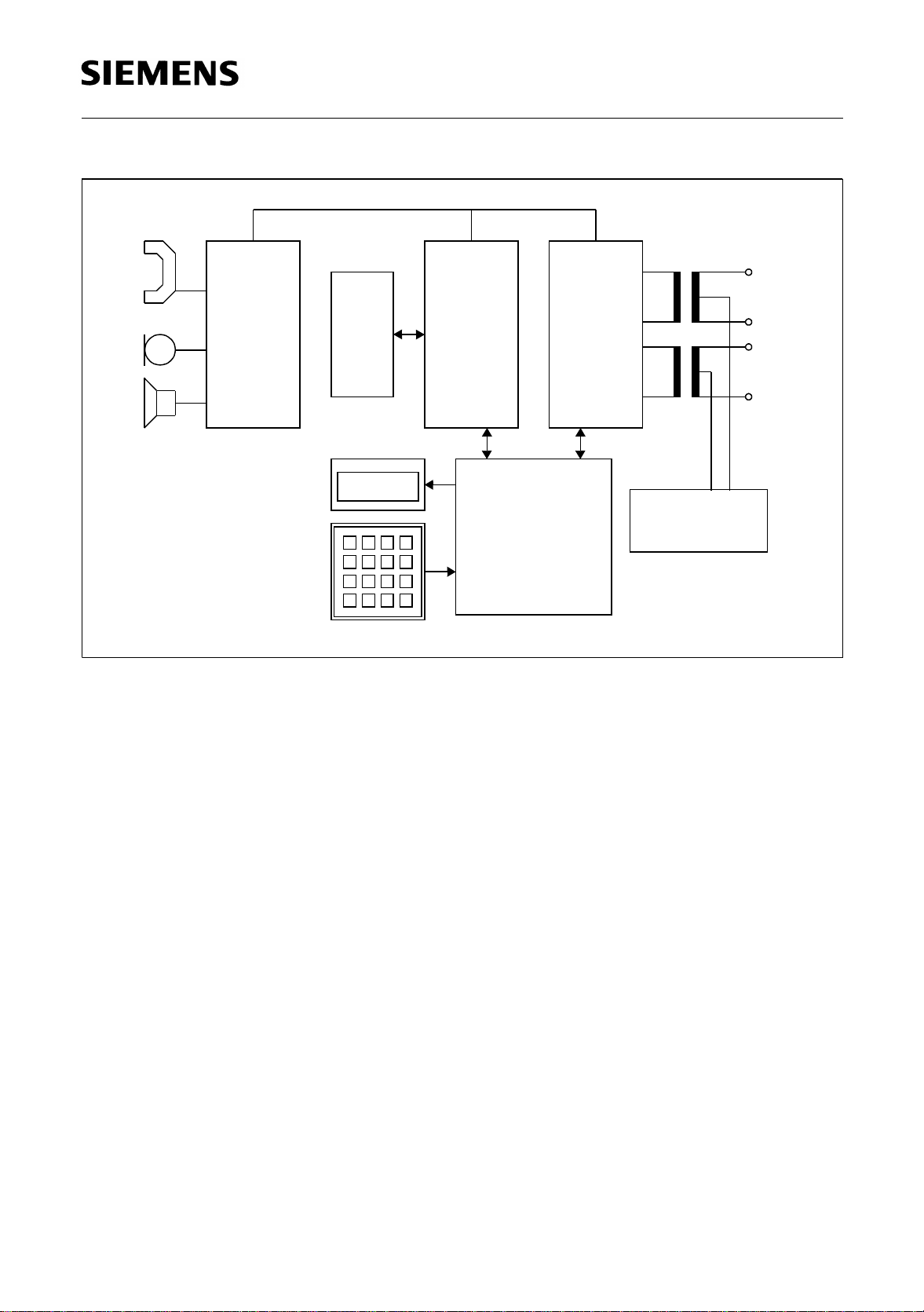
1.6.1 Stand-Alone Answering Machine
The PSB 2168 can also be used in con junction with a simple codec for a s tand-alone
answering machine (figure 5). In this application the PSB 2168 generates the necessary
clocks for the simple codec at the pins AFECLK and AFEFS. Therefore the simple codec
can be connected without further glue logic.
AFECLK
CLK
DCL
ARAM
DR
PSB 2168
DX
FSC
AFEFS
Microcontroller
line
tip/
ring
analog
simple
codec mux/amp
TX
TR
FS
077-3445
Figure 5 Stand-Alone Answering Machine with ARAM/EPROM
Voice Prompt
EPROM
Semiconductor Group 19 11.97
PSB 2168
Overview
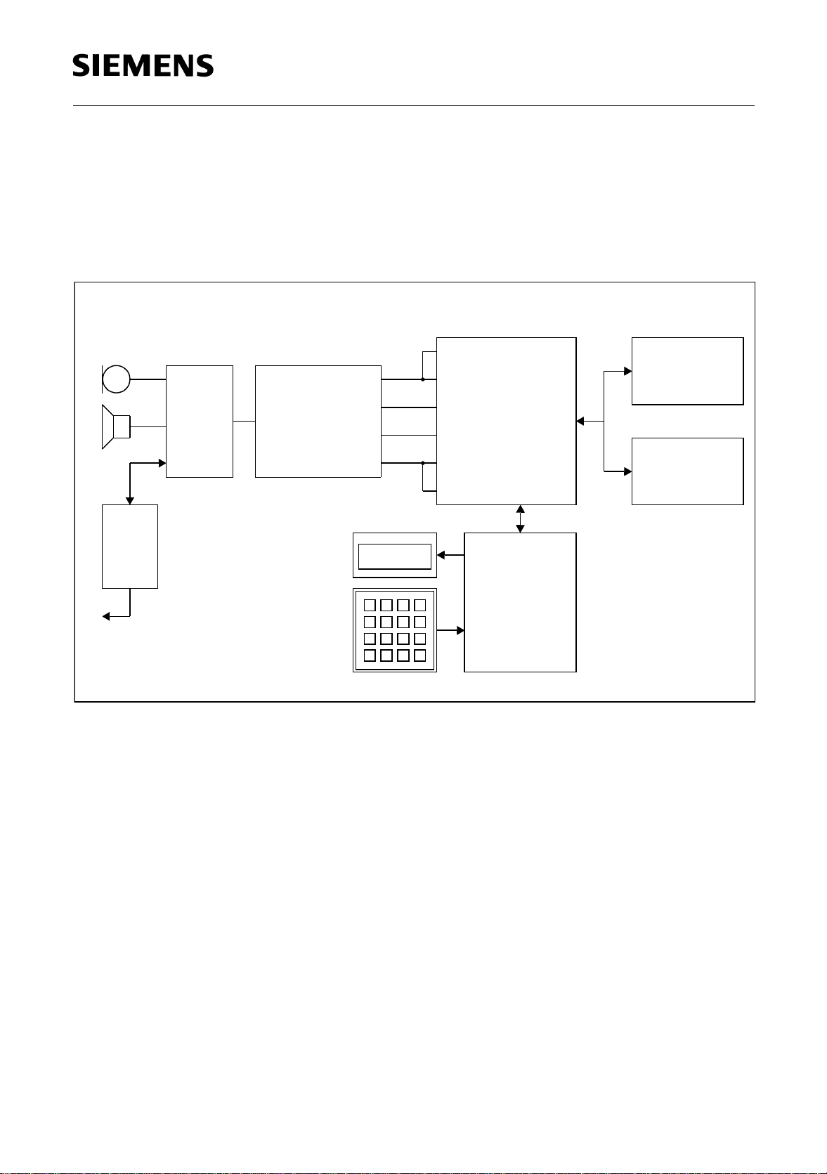
Furthermore the PSB 2168 can b e used to scan the keyboard and drive the display if
instead of ARAM/DRAM and EPROM flash memory devices (SAMSUNG mode) are
used for storage (figure 6).
®
-2
IOM
analog
tip/
ring
line
simple
codec mux/amp
PSB 2168
AFE
077-3445
Microcontroller
Figure 6 Stand-Alone Answering Machine with Flash Memory
In either case all features of the PSB 2168 can be used (e.g. caller id).
Flash
Semiconductor Group 20 11.97
PSB 2168
Functional Description
2 Functional Description
Functional Units
Functional Units
The PSB 2168 contains several functional units that can be combined wit h almost no
restrictions to perform a given task. Figure 7 gives an overview of the important
functional units.
SSDI/IOM®-2 IOM®-2
Channel 2Channel 1
DTMF
Generator
S
I1I2I
5
I
1
Universal
Attenuator
S
6
3
I1I
Line Echo
Canceller
S
8
S
I1I2I
7
3
S
13
Speech
Decoder
Memory
Speech
Coder
I1I
2
2
I1I
2
AGC
I
1
Equalizer
S
S
10
9
I
1
CNG
Detector
S
14
I
1
Alert Tone
Detector
S
15
I
1
CPT
Detector
S
S
17
16
I
1
CID
Decoder
S
18
I
1
DTMF
Detector
SCI
signal summation: s igna l sou rc es:
I
1
I
2
I
3
S
,...,S
5
18
Figure 7 Functional Units - Overview
Semiconductor Group 21 11.97

PSB 2168
Functional Description
Each unit has one or more signa l inputs (denoted by I). Most units have at least one
signal output (denoted by S). Any input I can be co nnected to any signal output S. In
addition to the sign als shown in figure 7 there is also the signal S
useful at signal summation points. Table 2 lists the available signals within the PSB 2168
according to their reference points.
Table 2 Signal Summary
Signal Description
(silence), which is
0
S
S
S
S
S
S
S
S
S
S
S
S
S
S
S
0
1
2
3
4
5
6
7
8
9
10
11
12
13
14
Silence
Reserved
Reserved
Reserved
Reserved
Serial interface input, channel 1
Serial interface output, channel 1
Serial interface input, channel 2
Serial interface output, channel 2
DTMF generator output
DTMF generator auxiliary output
Reserved
Reserved
Speech decoder output
Universal attenuator output
S
15
S
16
S
17
S
18
Semiconductor Group 22 11.97
Line echo canceller output
Automatic gain control output (after gain stage)
Automatic gain control output (before gain stage)
Equalizer output
PSB 2168
Functional Description
The following figures show the connections for a typical state during operation. Units that
are not needed are not shown. Inputs that are not nee ded are connected to S
provides silence (denoted by 0). In figure 8 a phone conversation is currently in progress.
The speech coder is used to record the signals of both parties. The alert tone detector is
used to detect an alerting tone of an off-hook cal ler id request while the CID decoder
decodes the actual data transmitted in this case.
SSDI/IOM®-2 IOM®-2
Channel 2Channel 1
which
0
S
5
000 000
S
7
Memory
Speech
coder
AGC
CPT
detector
CID
decoder
DTMF
detector
SCI
Figure 8 Functional Units - Recording a Phone Conversation
Semiconductor Group 23 11.97
PSB 2168
Functional Description
2.1 Functional Units
In this section the functional units of the PSB 2168 are described in detail. The functional
units can be individually enabled or disabled.
2.1.1 Line Echo Canceller
The PSB 2168 contains an adaptive line echo cancella tion unit for the cancellation of
near end echoes. The unit h as two modes: normal an d extended. In normal mod e, the
maximum echo length is 4 ms. This mode is alway s available. In extended mode , the
maximum echo length is 24 ms. Extended mode cannot be used while the speech
encoder or slow playback is active.
The line echo cancellation unit is especially useful in front of the various detectors
(DTMF, CPT, etc.). A block diagram is shown in figure 9.
I
2
+
Σ
S
15
-
Adaptive
Filter
I
1
Figure 9 Line Echo Cancellation Unit - Block Diagram
The line echo cancelle r provides only one ou tgoing signal (S
signal would be identical with the input signal I
Input I
is usually connected to the l ine inpu t w hile inp ut I1 is connected to the outgoing
2
.
1
) as the other outgoing
15
signal.
In normal mode the adaption process can be controlled by three parameters: MIN, ATT
and MGN. Adaption takes only place if both of the following conditions hold:
I1 MIN>
1.
I1 I2–ATTMGN+–0>
2.
With the first con diti on ada ption to sma ll signal s can be avoid ed. The s econd condit ion
avoids adaption during double talk. The parameter ATT represents the echo loss
provided by external circuitry. The adaption stops if the power of the received signal (I2)
exceeds the power of the expected signal (I1-ATT) by more than the margin MGN.
Semiconductor Group 24 11.97
PSB 2168
Functional Description
Table 3 shows the registers associated with the line echo canceller.
Table 3 Line Echo Cancellation Unit Registers
Register # of Bits Name Comment Relevant
Mode
LECCTL 1 EN Line echo canceller enable both
LECCTL 1 MD Line echo canceller mode
LECCTL 5 I2 Input signal selection for I
LECCTL 5 I1 Input signal selection for I
LECLEV 15 MIN Minimal power for signal I
2
1
1
LECATT 15 ATT Externally provided attenuation (I
to I2) normal
1
both
both
normal
LECMGN 15 MGN Margin for double talk detection normal
Semiconductor Group 25 11.97
PSB 2168
Functional Description
2.1.2 DTMF Detector
Figure 10 shows a block dia gram of the D TMF det ector. The results of t he dete cto r are
available in the status register and a dedicated resul t register that can be re ad via the
serial control interface (SCI) by the external controller. All sixteen standard DTMF tones
are recognized.
I
1
DTMF
Recognition
SCI
Figure 10 DTMF Detector - Block Diagram
Table 4 to 6 show the associated registers.
Table 4 DTMF Detector Control Register
Register # of Bits Name Comment
DDCTL 1 EN DTMF detector enable
DDCTL 5 I1 Input signal selection
As soon as a v ali d DTMF tone is reco gnized, the st atus word and the DTM F tone code
are updated (table 5).
Table 5 DTMF Detector Results
Register # of Bits Name Comment
STATUS 1 DTV DTMF code valid
DDCTL 5 DTC DTMF tone code
DTV is set when a DTMF tone is recognized and reset when no DTMF tone is recognized
or the detector is disabled. The code for the DTMF tone is placed into the register
DDCTL. The registers DDTW and DDLEV hold parameters for detection (table 6).
Table 6 DTMF Detector Parameters
Register # of Bits Name Comment
DDTW 15 TWIST Twist for DTMF recognition
DDLEV 6 MIN Minimum signal level to detect DTMF tones
Semiconductor Group 26 11.97
PSB 2168
Functional Description
2.1.3 CNG Detector
The calling tone (C NG) detector c an detect the standard calling tone s of fax m achines
or modems. This helps to distinguish voice messages from data transfers. The result of
the detector is available in the status register that can be read via the serial control
interface (SCI) by the exte rnal con troller. The CNG d etector cons ists of tw o band-pas s
filters with fixed center frequency of 1100 Hz and 1300 Hz.
CNG Detector
I
1
1100 Hz 1300 Hz
SCI
Figure 11 CNG Detector - Block Diagram
Table 7 shows the available parameters.
Table 7 CNG Detector Registers
Register # of Bits Name Comment
CNGCTL 1 EN CNG detector enable
CNGCTL 5 I1 Input signal selection
CNGLEV 16 MIN Minimum signal level
CNGBT 16 TIME Minimum time of signal burst
CNGRES 16 RES Input signal resolution
Both the programmed mini mum time and the mi nimum signal level m ust be exceeded
for a valid CNG tone. Furthermore the input signal resolution can be reduced by the RES
parameter. This can be useful in a noisy env ironment at low signal levels although the
accuracy of the detect ion decreases. As soo n as a valid tone is recognized, t he status
word of the PSB 2168 is updated. The status bits are defined as follows:
Table 8 CNG Detector Result
Register # of Bits Name Comment
STATUS 1 CNG Fax/Modem calling tone detected
Semiconductor Group 27 11.97
PSB 2168
Functional Description
2.1.4 Alert Tone Detector
The alert tone detector can detect the st andard alert tones (2130 Hz and 27 50 Hz) for
caller id protocols. The results of the detector are available in the status register and the
dedicated regist er ATDCTL 0 that c an be re ad via the ser ial cont rol int erface (SCI) by the
external controller.
I
1
Detector
SCI
Figure 12 Alert Tone Detector - Block Diagram
Table 9 Alert Tone Detector Registers
Register # of Bits Name Comment
ATDCTL0 1 EN Alert Tone Detector Enable
ATDCTL0 5 I1 Input signal selection
ATDCTL1 1 MD Detection of dual tones or single tones
ATDCTL1 1 DEV Maximum deviation (0.5% or 1.1%)
ATDCTL1 8 MIN Minimum signal level to detect alert tones
Alert Tone
As soon as a valid alert tone is recognized, the status word of the PSB 2168 and the code
for the detected combination of alert tones are updated (table 10).
Table 10 Alert Tone Detector Results
Register # of Bits Name Comment
STATUS 1 ATV Alert tone detected
ATDCTL0 2 ATC Alert tone code
Semiconductor Group 28 11.97
PSB 2168
Functional Description
2.1.5 CPT Detector
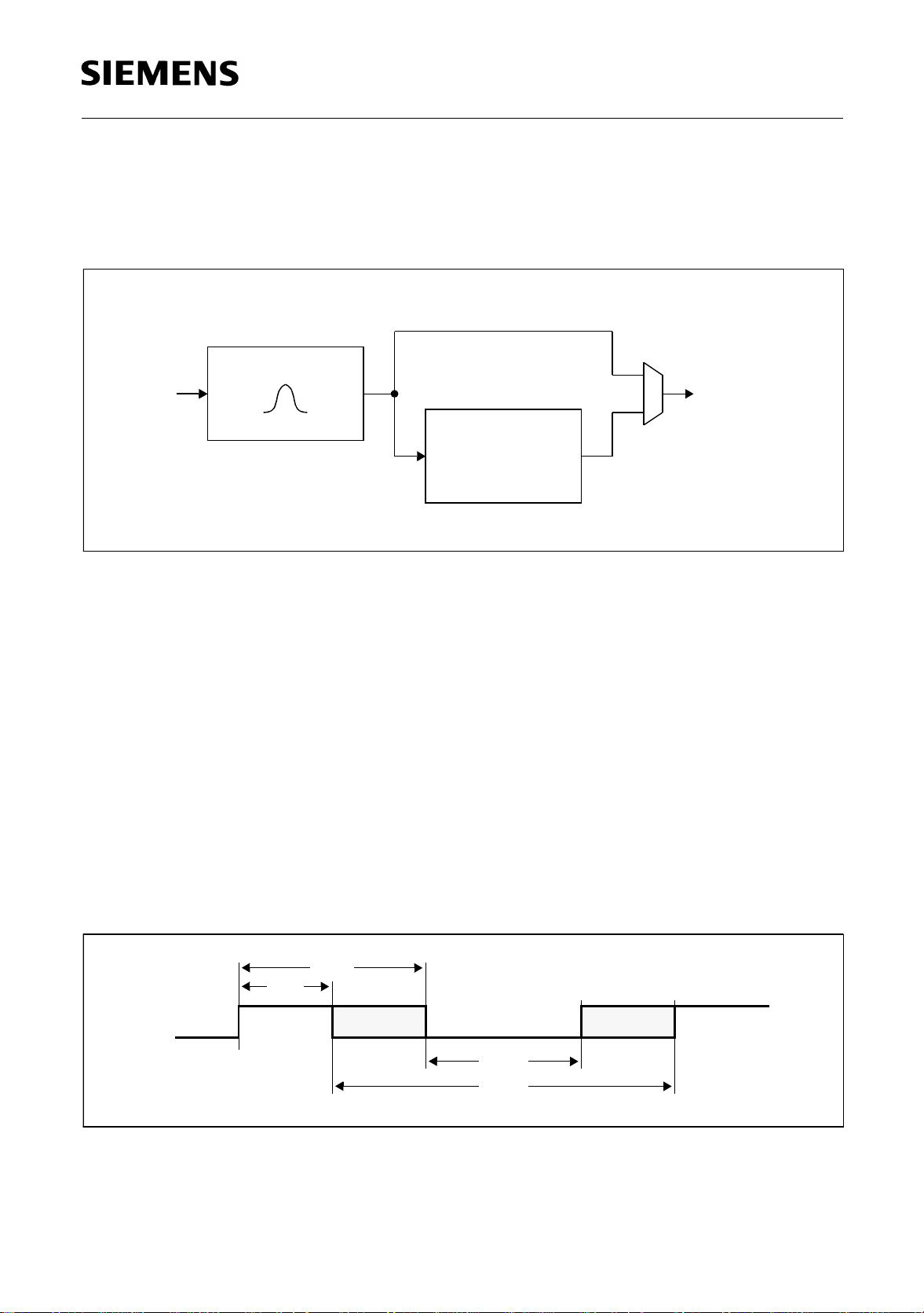
The selected signal is monitored continuously for a call progress tone. The CPT detector
consists of a band-pass and an optional timing checker (figure 13).
Band-pass
1
300-640 Hz
SCI (Status)I
Timing
Checker
Figure 13 CPT Detector - Block Diagram
The CPT detector can be used in two modes: raw and cooked. In raw mode, the
occurrence of a signal within the frequency range, time and energy limits is directly
reported. The timing checker is bypassed and therefore the PSB 2168 does not interpret
the length or interval of the signal.
In cooked mode, the number and duration of signal bursts are interpre ted by the timing
checker. A signal burst f ollowed by a gap is called a cycle. Cooked mode req uires a
minimum of two cycles. The CPT flag is set with the first burst after the programmed
number of cycles has been detected. The CPT flag remains set until the unit is disabled,
even if the conditions are not met anymore. In this mode the CPT is modelled as a
sequence of identical bursts separated by gaps with identical length. The PSB 2168 can
be programmed to accept a range for bo th the burst and the gap. It is also poss ible to
specify a maximum aberration of two consecutive bursts and gaps. Figure 14 shows the
parameters for a single cycle (burst and gap).
t
Bmin
Bmax
t
Gmin
t
Gmax
t
Figure 14 CPT Detector - Cooked Mode
The status bit is defined as follows:
Semiconductor Group 29 11.97

PSB 2168
Functional Description
Table 11 CPT Detector Result
Register # of Bits Name Comment
STATUS 1 CPT CP tone currently detected [340 Hz; 640 Hz]
CPT is not affected by reading the status word. It is automatically reset when the unit is
disabled. Table 12 shows the control register for the CPT detector.
Table 12 CPT Detector Registers
Register # of Bits Name Comment
CPTCTL 1 EN Unit enable
CPTCTL 1 MD Mode (cooked, raw)
CPTCTL 5 I1 Input signal selection
CPTMN 8 MINB Minimum time of a signal burst (t
CPTMN 8 MING Minimum time of a signal gap (t
Gmin
CPTMX 8 MAXB Maximum time of a signal burst (t
CPTMX 8 MAXG Maximum time of a signal gap (t
Bmin
Bmax
Gmax
)
)
)
)
CPTDT 8 DIFB Maximum difference between con secutive bursts
CPTDT 8 DIFG Maximum difference between consec uti ve gaps
CPTTR 3 NUM Number of cycles (cooked mode), 0 (raw mode)
CPTTR 8 MIN Minimum signal level to detect tones
CPTTR 4 SN Minimal signal-to-noise ratio
If any condition is violated during a sequen ce of c ycles t he timing checke r is reset and
restarts with the next valid burst.
Note: In cooked mode CPT is set with the first burst after the pro grammed number of
cycles has been detected.
Note: The number of cycles must be set to zero in raw mode.
Semiconductor Group 30 11.97
 Loading...