

General-Purpose Power Controller
(GPPC)
Features
● Switched mode DC/DC-converter
● CCITT ISDN compatible
● Low power dissipation
● Supply voltage range 8 to 70 V
● Programmable input undervoltage protection
● Programmable overcurrent protection
● Soft start
● Power housekeeping input
● Oscillator synchronization input/output
● High voltage CMOS-technology 70 V
PSB 2121
CMOS IC
P-DSO-20-1
P-DIP-16
Type Version Ordering Code Package
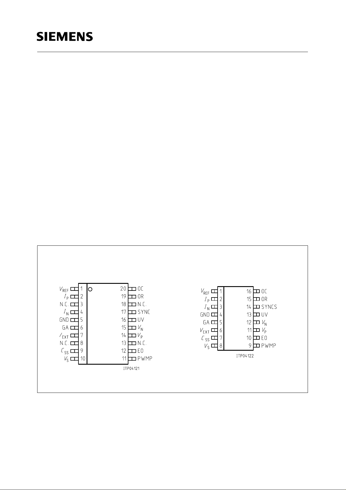
PSB 2121-P V A4/A5 Q67100-H8646 P-DIP-16
PSB 2121-T V A4/A5 Q67100-H6032 P-DSO-20-1 (SMD)
The PSB 2121 is a pulse width modulator circuit designed for fixed-frequency switching regulators
with very low power consumption.
In telephony and ISDN systems a high conversion yield is crucial to maintain functionality in all
supply conditions via “S” or “U” interfaces. The PSB 2121 design and technology realize high
conversion efficiency and low power dissipation.
It should be recognized that the PSB 2121 can also be used in numerous DC/DC-conversion
systems other than ISDN-power supplies.
Semiconductor Group 1 12.92
PSB 2121
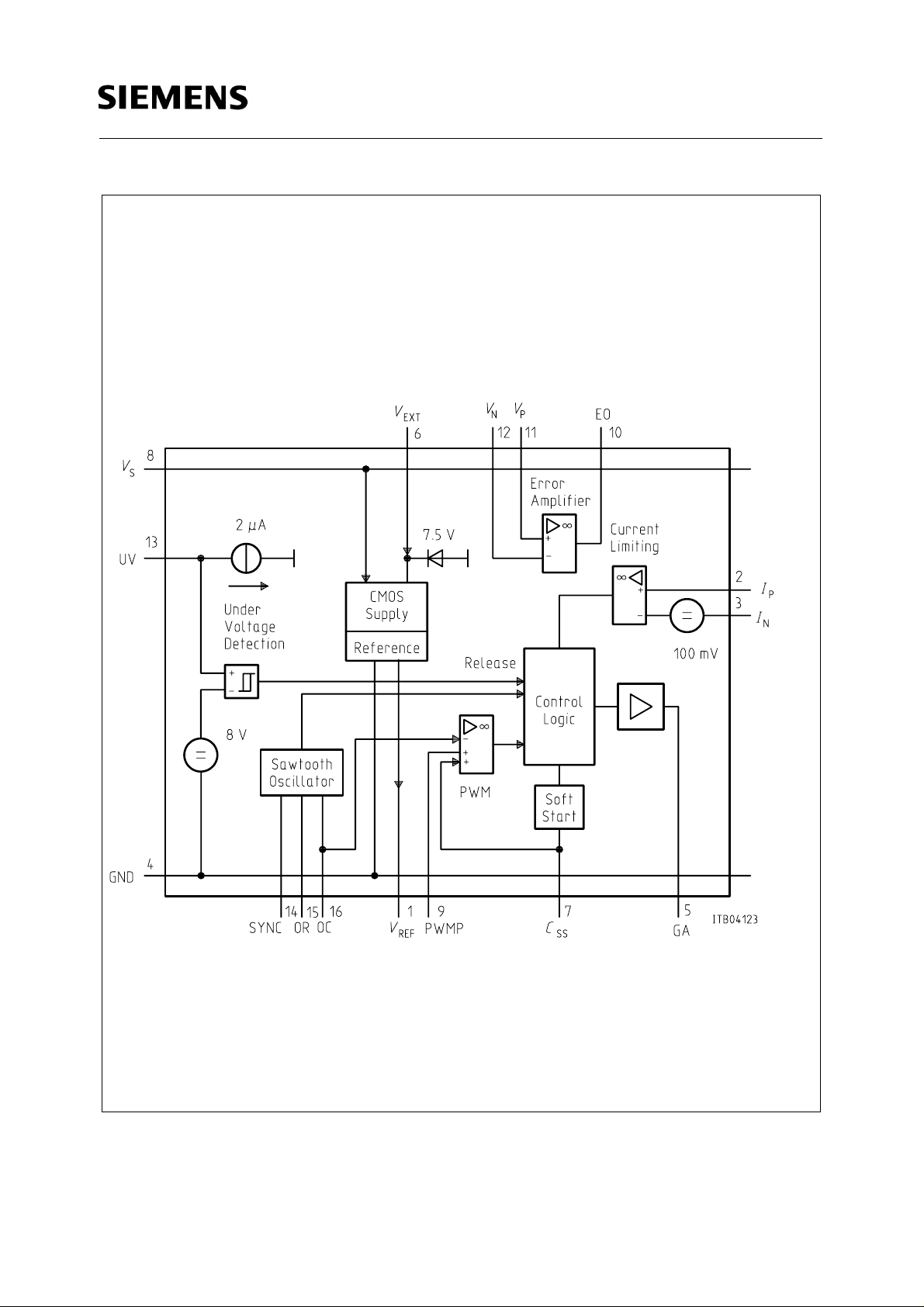
The PSB 2121 Contains the Following Functional Blocks
● Undervoltage lockout
● Temperature compensated voltage reference
● Sawtooth oscillator
● Error amplifier
● Pulse width modulator
● Digital current limiting
● Soft start
● Double pulse inhibit
● Power driver
Together with few external components it provides a stable 5 V DC-supply for subscriber terminals
(TEs) or network terminations (NTs). It can also be programmed for higher output voltages, e.g. to
supply S-lines with 40 V.
Pin Configurations
(top view)
P-DIP-16P-DSO-20
Semiconductor Group 2

Pin Definitions and Functions
PSB 2121
Pin No.
P-DSO
11
22
43
Pin No.
P-DIP
Symbol Input (I)
Output (O)
V
REF
I
P
I
N
O Reference
I Positive current
I Negative
Definition Function
Output of the 4.0 V reference
voltage
voltage.
When the voltage difference
sense
between these two pins exceeds
100 mV, the digital current limiting
current sense
becomes active.
5 4 GND I Ground All analog and digital signals are
referred to this pin.
6 5 GA O Gate Totem-pole output driver, has to be
connected with the gate of an
external power switch.
76
V
EXT
I/O External supply Output of the internal CMOS
supply. Via
V
the internal CMOS-
EXT
circuits can be supplied from an
external DC-supply in order to
reduce chip power dissipation.
97
C
SS
I Soft start
capacitor
The capacitor at this pin determines
the soft start characteristic.
10 8
11 9 PWMP I Pulse width
V
S
I Battery voltage VS is the positive input voltage.
Non-inverting input of the pulse
modulator
width modulator.
12 10 EO O Error amplifier output.
14 11
15 12
V
P
V
N
I Positive
voltage sense
I Negative
Non-inverting input of the error
amplifier.
Inverting input of the error amplifier.
voltage sense
16 13 UV I Undervoltage
detection
The undervoltage lockout can be
programmed via UV.
17 14 SYNC I/O Synchronization This pin can be used as an input for
synchronization of the oscillator to
an external frequency, or as an
output to synchronize multiple
devices.
19 15 OR I R-oscillator The external timing components of
20 16 OC I C-oscillator
the ramp generator are attached to
OR and OC.
Semiconductor Group 3
PSB 2121
Figure 1
GPPC Functional Diagram
Semiconductor Group 4

PSB 2121
Absolute Maximum Ratings
Parameter Symbol Limit Values Unit
V
Supply voltage (pin
) referred to GND V
S
Analog input voltage
(pins
I
, IN, PWMP, VP, VN, SYNC, OR, OC)
P
referred to GND
V
Reference output current (pin
) I
REF
SYNC output current (pin SYNC)
Error amplifier output current (pin EO)
Z-current (pin
Output current (pin
V
) I
EXT
V
) I
EXT
Driver output current (pin GA)
Ambient temperature under bias
Storage temperature
S
V
I A
O REF
I
O SYNC
I
O Amp
Z EXT
O EXT
I
D R
T
A
T
stg
80 V
6V
–5 mA
–5 mA
–5 mA
2mA
–5 mA
–5 mA
– 25 to 85 ˚C
– 40 to 125 ˚C
DC-Characteristics
T
= 0 to 70 ˚C, VS = 9 to 70 V
A
Parameter Symbol
Supply current
Reference
V
REF
Output voltage V
Line regulation
Load regulation
Temperature stability
Load current
I
S
REF O
V
REF Line
V
REF Load
V
REF TS
I
REF Load
Limit Values
Unit Test Conditionmin. typ. max.
30 50 µA V
S EXT
≥ 6.2 V
3.92 4.0 4.08 V TA = 25 ˚C
I
= 0 mA,
L
V
= 40 V
S
60 mV VS = 20 to 60 V
T
= 25 ˚C
A
I
= 0 mA
L
20 40 mV IL = 0.1 to 0.3 mA
V
= 40 V,
S
T
= 25 ˚C
A
25 mV 0…70˚C
0.5 mA
Semiconductor Group 5

DC-Characteristics (cont’d)
PSB 2121
Limit Values
Parameter Symbol
Oscillator / SYNC / OC
f
= 20 kHz, RT = 39 kΩ± 1%, RD = 0 Ω, CT = 1 nF ± 1%
OSC
Initial accuracy T
= 25 ˚C
A
Voltage stability
Temperature stability
Max. frequency
Sawtooth peak voltage
Sawtooth valley voltage
H-sync output level
L-sync output level
V
Error Amplifier / EO /
/ V
P
Input offset voltage V
Input current
Common mode range
f
max
V
S
V
S
V
SYNC H
V
SYNC L
N
IO
I
I
CMR
200 250 kHz RT = 27 kΩ
3.0
1.6
2.4 3.5
1.8 4.5 V
Unit Test Conditionmin. typ. max.
± 10
1
5
3.2
1.8
0.2
3
5.25
0.8
%
%
%
V
V
V
V
C
T
I
= − 0.5 mA
L
V
EXT
I
= 20 µA
L
310mV
25 nA
= 39 pF
= ≤ 6.3 V
DC open loop gain
Common mode rejection
Unity gain bandwidth
Supply voltage rejection
H-output voltage
L-output voltage
Current Limit Comparator
T
= 25 ˚C
A
Sense voltage
Input bias current
Input voltage range
Response time
(signal at GA)
I
P
/ IN,
G
k
f
k
V
V
V
I
V
t
VO
CMR
SVR
OH
OL
Sense
I
I
Res
60 70 dB
60 70 dB
0.5 1 MHz CL (pin) ≤ 10 pF
60 70 dB
4 5.5
0.02 1
V
V
I
= – 100 µA
L
I
= 10 µA
L
85 100 115 mV VS = 40 V
0 100 nA
01V
12µs IN = 0 V
I
= 0 → 200 mV
P
Semiconductor Group 6

DC-Characteristics (cont’d)
PSB 2121
Limit Values
Parameter Symbol
Pulse Width Modulator
Duty cycle
t
d
Under Voltage Detection UV
Start up threshold
Threshold hysteresis H
Soft Start C
SS
Charging current C
V
y
T
Output Driver GA
T
= 25 ˚C
A
H-output voltage
L-output voltage
Rise time
Fall time
Output current
V
OH
V
OL
t
r
t
f
I
O
Unit Test Conditionmin. typ. max.
050%
789Vpin UV = V
0.3 V pin UV = V
248µA
4.5 V
0.3 0.4 V I
EXT
V I
Source
= 5 mA
Sink
= 5 mA
130 200 ns CL = 220 pF;
V
= 6.3 V
EXT
70 200 ns CL = 220 pF;
V
= 6.3 V
EXT
5mA
S
S
External Supply
Output voltage V
Output current
Input voltage
Z-current
Power consumption
V
EXT
O
I
O
V
I
I
Z
P
tot
6.0 7.5 V
Semiconductor Group 7
5.8 V
2mA
2mA
56mWVS = 40 V
f
= 20 kHz
OSC
V
= 6.2 to 6.7 V
EXT

PSB 2121
Application Informations
Undervoltage Lockout
The undervoltage lockout circuit protects the PSB 2121 and the power devices from inadequate
supply voltage. If
functions have been stabilized in the proper state when the turn on voltage (8 V) is reached, and it
prevents from the possibility of start up glitches. The undervoltage lockout is programmable by
connecting a Z-diode between
undervoltage lockout is 8 V.
Voltage Reference
The reference regulator of the PSB 2121 is based on a temperature compensated bandgap. This
circuitry is fully active at supply voltages above + 6.0 volts and provides up to 0.5 mA of load current
to external circuitry at + 4.0 volts. This reference has to be buffered by an external capacitor
> 0.5 µF.
V
is too low, the circuit disables this output driver. This ensures that all control
S
V
and UV from 8 V up to 70 V. If UV is connected to VS the default
S
Oscillator
The oscillator frequency is programmed by three components:
The oscillator timing capacitor
C
is charged by V
T
through RT and discharged by RD. (RD is series-
REF
R
, CT and RD as shown in figure 2.
T
connected with an internal 9 kΩ discharge-resistor.) So the rise-time and the fall-time of the
sawtooth oscillator can be programmed individually.
Figure 2
Semiconductor Group 8

PSB 2121
At the beginning of the discharge period a positive synchronization pulse is generated at pin SYNC.
Otherwise the PSB 2121 can be synchronized via pin SYNC to an external logic clock by
programming the oscillator to free run at a frequency 10 % lower than the synchronization
frequency. The PSB 2121 is synchronized by the rising edge of the sync. signal. So multiple devices
can be synchronized together by programming one master unit for the desired frequency.
Notice that the frequency of the output driver is half the oscillator frequency. The switching
frequency as a function of RT and CT with RD = 0 is shown in figure 3.
Figure 3
Switching Frequency
Soft Start Circuit
The soft start circuit protects the power transistors and rectifier diodes from high current surges
during power supply turn-on. When the supply voltage is connected to the PSB 2121 the
undervoltage lockout circuit holds the soft start capacitor voltage at zero. When the supply voltage
reaches normal operating range an internal 4 µA current source will charge the external soft start
capacitor. As the soft start voltage ramps up to + 5 volts, the duty cycle of the PWM linearly
increases to whatever value the regulation loop requires.
Semiconductor Group 9

PSB 2121
Pulse Width Modulator
The pulse width modulator compares the sawtooth-voltage of the oscillator output with the input
signal at PWMP and with the voltage of the external soft start capacitor at CSS (see figure 1).
Error Amplifier
Conventional operational amplifier for closed-loop gain and phase compensation.
Low output impedance: unity-gain stable
Control Logic
The control logic inhibits double pulses during one duty cycle and limits the maximum duty cycle to
50 %.
Current Limiting
A differential input comparator terminates individual output pulses each time when the sensvoltage
rises above threshold.
When sense voltage rises to 100 mV above threshold a shutdown signal is sent to the control logic.
CMOS Supply
An integrated 6 V linear voltage regulator supplies the internal low-voltage CMOS-circuits from the
input voltage. This supply-voltage is connected to pin
capacitor (
C
= 1 µF). Power dissipation of the linear voltage regulator can be reduced, if an
min
external supply is used for that purpose by connecting it to pin
V
and has to be buffered by an external
EXT
V
. If the input voltage at V
EXT
EXT
reaches 6.2 V the internal linear voltage regulator turns off and the internal CMOS-circuits are fed
from the external voltage. In this case the input current at
V
Note:An internal 7.5 V Z-diode protects the
input against overvoltage. The maximum Z-current
EXT
V
is approx. 0.5 mA.
EXT
is 2 mA! So if the external CMOS-supply isn’t stabilized the input current must be limited (e. g.
by a resistor).
Semiconductor Group 10

PSB 2121
Extended Input Voltage Range
Some DC/DC-converter applications require a higher input voltage than the maximum supply
voltage of the PSB 2121 which is limited to 70 V. Figure 4 shows a method to extend the input
voltage range by connecting a zener-diode between the input voltage and
V
of the PSB 2121.
S
Figure 4
If the PSB 2121 is fed via
losses are accordingly 30 µA ×
V
, the input current at pin VS is approx. 30 µA. The additional power
EXT
V
; the minimum input voltage is VZ +8V.
Z
PSB 2121 Applications
The PSB 2121 accommodates both galvanically isolated and non-isolated configurations.
Figure 5 shows a non-isolated 1 W flyback converter. The converter is fully compatible with the
CCITT-power recommendations on the S-interface. At an input voltage of 40 V, the efficiency is
64 % at an input power of 250 mW and 86 % at an input power of 900 mW.
Figure 6 shows a 4 W flyback converter with opto isolation to feed the S-bus with 40 V. The
maximum input voltage is extended from 70 V to 100 V.
Semiconductor Group 11

PSB 2121
Figure 5
Application Circuit
Semiconductor Group 12

PSB 2121
Figure 6
Application Circuit
Semiconductor Group 13
 Loading...