

Siemens PSB2120-P, PSB2120-T Datasheet
ISDN Remote Power Controller
(IRPC)
Features
● Switched mode DC/DC-converter
● Switched mode DC/DC-converter
● CCITT (I.430) ISDN compatible
● Integrated 200 V power FET
(only PSB 2120-P in P-DIP-22)
● Low power dissipation
● Supply voltage range 10 V to 60 V
● Input undervoltage detection
● Programmable overcurrent protection
● Soft start
● Control circuit to achieve minimum start-up current
● Power housekeeping input
● Oscillator synchronization input/output
● Polarity reversal detection
● High voltage CMOS-technology 60 V
PSB 2120
CMOS IC
P-DSO-24-1
P-DIP-22
Type Version Ordering Code Package
PSB 2120-P V B5 Q67100-H8645 P-DIP-22
PSB 2120-T V B5 Q67100-H6278 P-DSO-24-1 (SMD)
The PSB 2120 is a Pulse Width Modulator (PWM) circuit designed for fixed-frequency switching
regulators especially for telephony and ISDN-environments.
The PSB 2120 is fully compatible with the CCITT-power recommendations on the “S”-interface.
Coupled with a few external components it can provide a stable 5 V DC-supply for subscriber
terminals (TE’s) or network terminators (NT’s). It can also be programmed for higher output
voltages, e.g. to supply the S-lines with 40 V.
In telephony and ISDN-systems a high conversion yield is crucial to maintain functionality in all
supply conditions via “S”- or “U”-interfaces. The PSB 2120 design and technology realizes high
conversion efficiency and low power dissipation.
It should be recognized that the PSB 2120 can also be used in numerous DC/DC-conversion
systems other than ISDN-power supplies.
Semiconductor Group 3 12.92
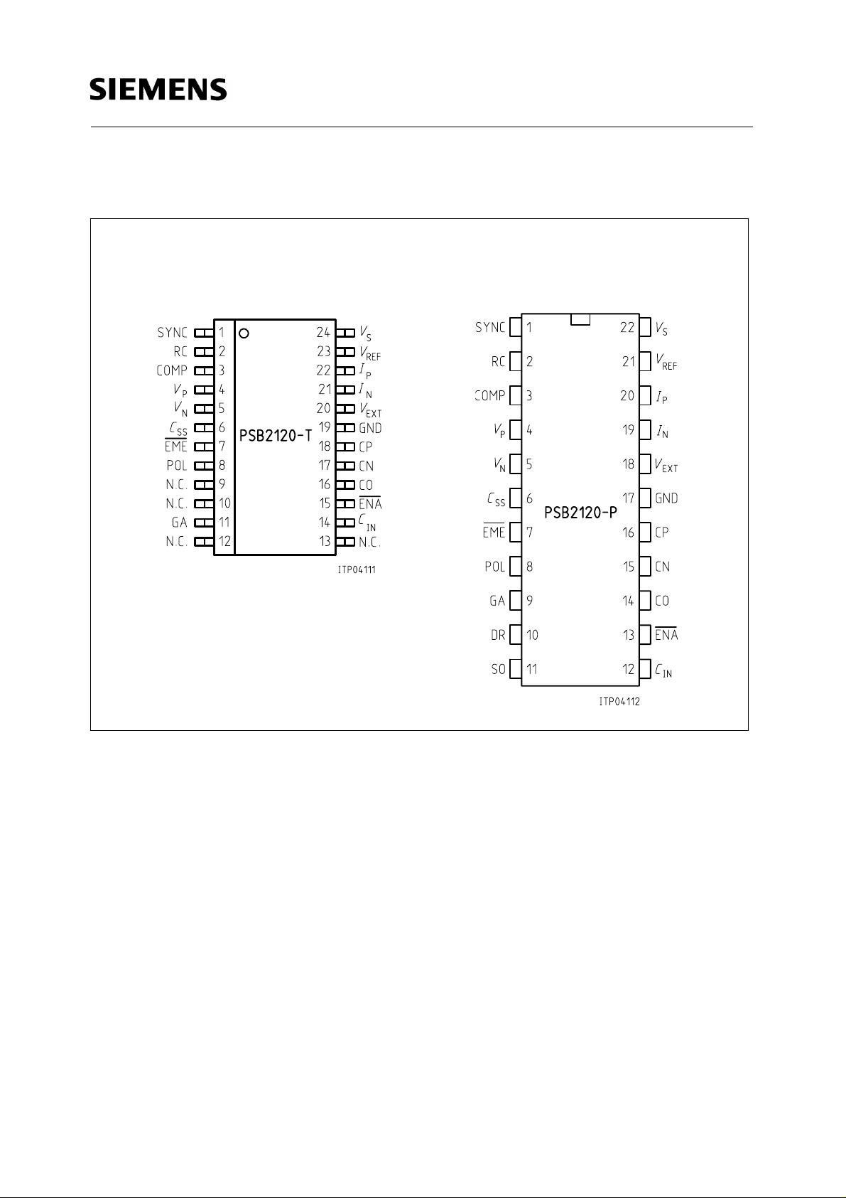
Pin Configurations
(top view)
PSB 2120
P-DSO-24 P-DIP-22
Semiconductor Group 2

Pin Definitions and Functions
PSB 2120
Pin
No.
P-DSO
Pin
No.
P-DIP
Symbol Input (I)
Output (O)
Definition Function
1 1 SYNC I/O Synchronization Input for synchronization of the
oscillator to an external frequency,
or output to synchronize multiple
devices.
2 2 RC I RC-Oscillator The external timing components of
the ramp generator are attached to
this pin.
3 3 COMP O Compensation Error amplifier output and Pulse
Width Modulator (PWM) input for
loop stabilization network.
44
55
V
P
V
N
I Positive Voltage
Sense
I Negative Voltage
Non-inverting input of the error
amplifier.
Inverting input of the error amplifier.
Sense
66
77
C
SS
EME O Emergency A low input voltage at POL will
I Soft Start
Capacitor
The capacitor at this pin determines
the soft-start characteristic.
activate the output
EME.
8 8 POL I Polarity
Detection
POL is the input to a non inverting
Schmitt-trigger.
11 9 GA O Gate Output of the FET-driver.
N.C. 10 DR O Drain Drain connection of the power FET.
N.C. 11 SO O Source Source connection of the power
FET.
14 12
C
IN
I Input Capacitor CIN has to be connected to the input
buffer-capacitor and a current
limiting charging-resistor.
Semiconductor Group 3

Pin Definitions and Functions (cont’d)
PSB 2120
Pin
No.
P-DSO
15 13
Pin
No.
P-DIP
Symbol Input (I)
Definition Function
Output (O)
ENA I Enable A high input voltage at this pin will
stop the IRPC-function.
16 14 CO O Comparator
output
17 15 CN I Comparator
neg. input
Connections of the universal usable
comparator.
18 16 CP I Comparator
pos. input
19 17 GND I Ground All analog and digital signals are
referred to this pin.
20 18
V
EXT
I/O External supply Output of the internal CMOS-supply.
Via
V
the internal CMOS-circuits
EXT
can be supplied from an external
DC-supply in order to reduce chip
power dissipation.
21 19
22 20
I
N
I
P
I Negative current
sense
I Positive current
sense
When the voltage difference
between these two pins exceeds
100 mV, the digital current limiting
becomes active.
23 21
24 22
V
REF
V
S
O Reference
voltage
I Supply voltage V
Output of the 4.0 V reference
voltage.
is the positive input voltage.
BAT
Semiconductor Group 4
PSB 2120
Figure 1
IRPC Functional Diagram
Semiconductor Group 5

PSB 2120
Functional Description
The reference provides a 4.0 V voltage for the regulation loop. A high gain error amplifier compares
the reference voltage with the switch mode supply output voltage. The output of the error amplifier
is compared with a periodic linear ramp, which is generated by the sawtooth-oscillator circuit. The
comparator output is a fixed-frequency, variable pulse width logic signal, which passes through
logic circuits to the high voltage power-switching-FET.
A digital current limiting device suppresses the PWM logic signal when the voltage difference at the
current limit sense input reaches 100 mV. In this case the control logic inhibits double pulses during
one oscillator period.
Start-Up Procedure
Before the switched-mode DC/DC-converter starts, a sequence of several conditions has to be
passed in order to avoid any system malfunction.
The primary undervoltage detection inhibits the converter function. This insures that all control
functions have stabilized in the proper state when the turn on voltage (ca. 10 V) is reached, and it
prevents start-up glitches.
In case of connecting the TE to powered lines or if a line is powered up, the charge current of the
primary buffer capacitor is limited by an external resistor (figure 2).
This resistor is short-circuited by the PSB 2120 when the voltage drop across it falls below
approximately 2.0 V. The residual resistance of this short-circuit is about 3 Ω. In case of a primary
undervoltage detection the short-circuit will be always deactivated. So, the DC/DC-converter does
not start until the charging of the primary buffer capacitor is completed, and the maximum line input
voltage is reached. If this feature is not desired,
C
has to be connected to GND. In this case the
IN
primary current measuring circuit turns off, to reduce chip-power dissipation from 9 mW to 6 mW.
In order to avoid high current peaks during the charging of the secondary capacitors or line
capacitors in case of supplying an S-interface, a soft start circuit is implemented in the PSB 2120.
This circuit requires an external capacitor, connected between
In addition, the enable input (
converter is disabled via
ENA) allows an external switch-on/switch-off control. If the DC/DC-
ENA, the soft-start-capacitor at pin CSS is discharged. This input can also
C
and GND.
SS
be used for several other functions, e.g. secondary overvoltage protection.
Semiconductor Group 6
 Loading...