

Page 1
MULTIMOBIL 2.5
Wiring Diagrams
SP
© Siemens AG 2003
The reproduction, transmission or
use of this document or its contents
is not permitted without express
written authority. Offenders will be
liable for damages. All rights,
including rights created by patent
grant or registration of a utility
model _or_ design,_are_ reserved.
English
Print No.: SPR8-X01.844.01.02.02 Doc. Gen. Date: 09.05
Replaces: SPR8-X01.844.01.01.02
Page 2
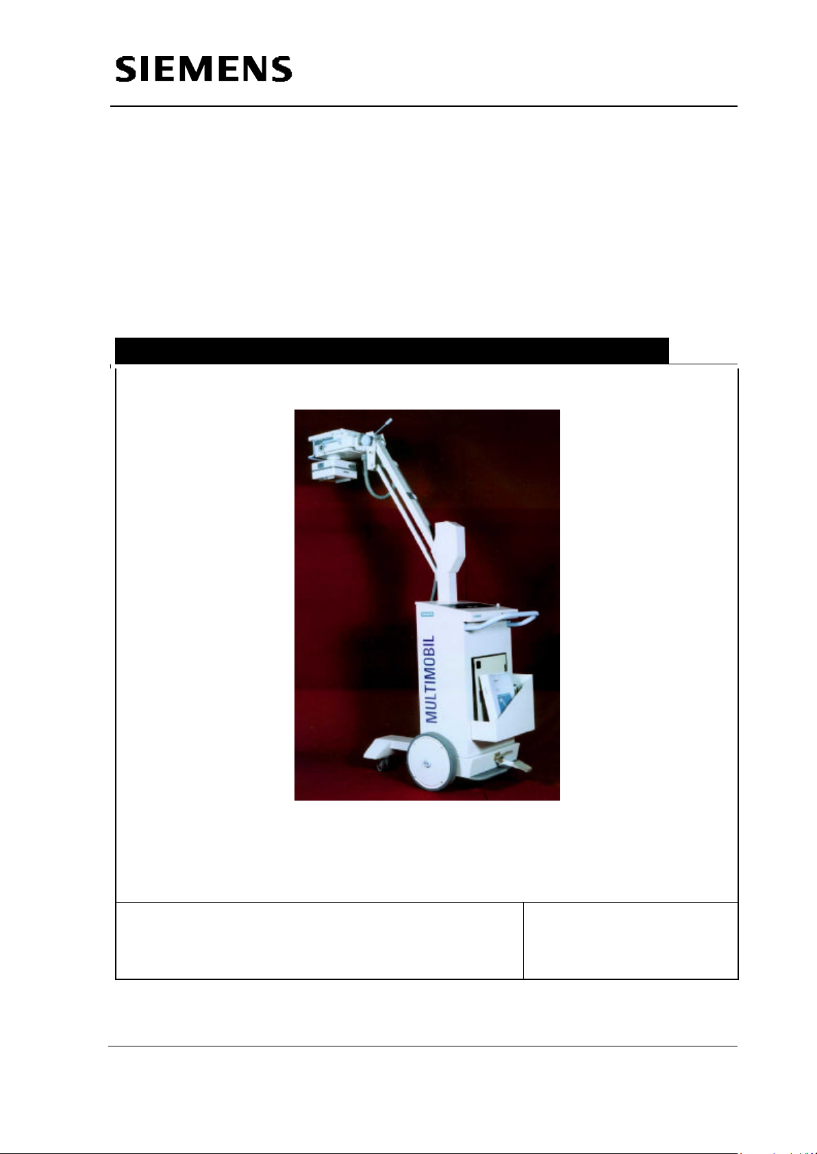
Multimobil 2.5
Copyright SIEMENS LTD.,MED INDIA
Service Manual
Circuit Diagrams
Med
Circuit Diagrams
Version: 6.0
Siemens Ltd. Med India Version 6.0
Copyright SIEMENS LTD. All rights reserved. For internal use only
The reproduction, transmission or use of
this document or its contents is not
permitted without express written
authority. Offenders will be liable for
damages.
5-1
Page 3

Service Manual
Circuit Diagrams
Index
5 CIRCUIT DIAGRAMS.............................................................................................................................................5-4
Siemens Ltd. Med India Version 6.0
Copyright SIEMENS LTD. All rights reserved. For internal use only
5-2
Page 4

Service Manual
Circuit Diagrams
Siemens Ltd. Med India Version 6.0
Copyright SIEMENS LTD. All rights reserved. For internal use only
5-3
Page 5
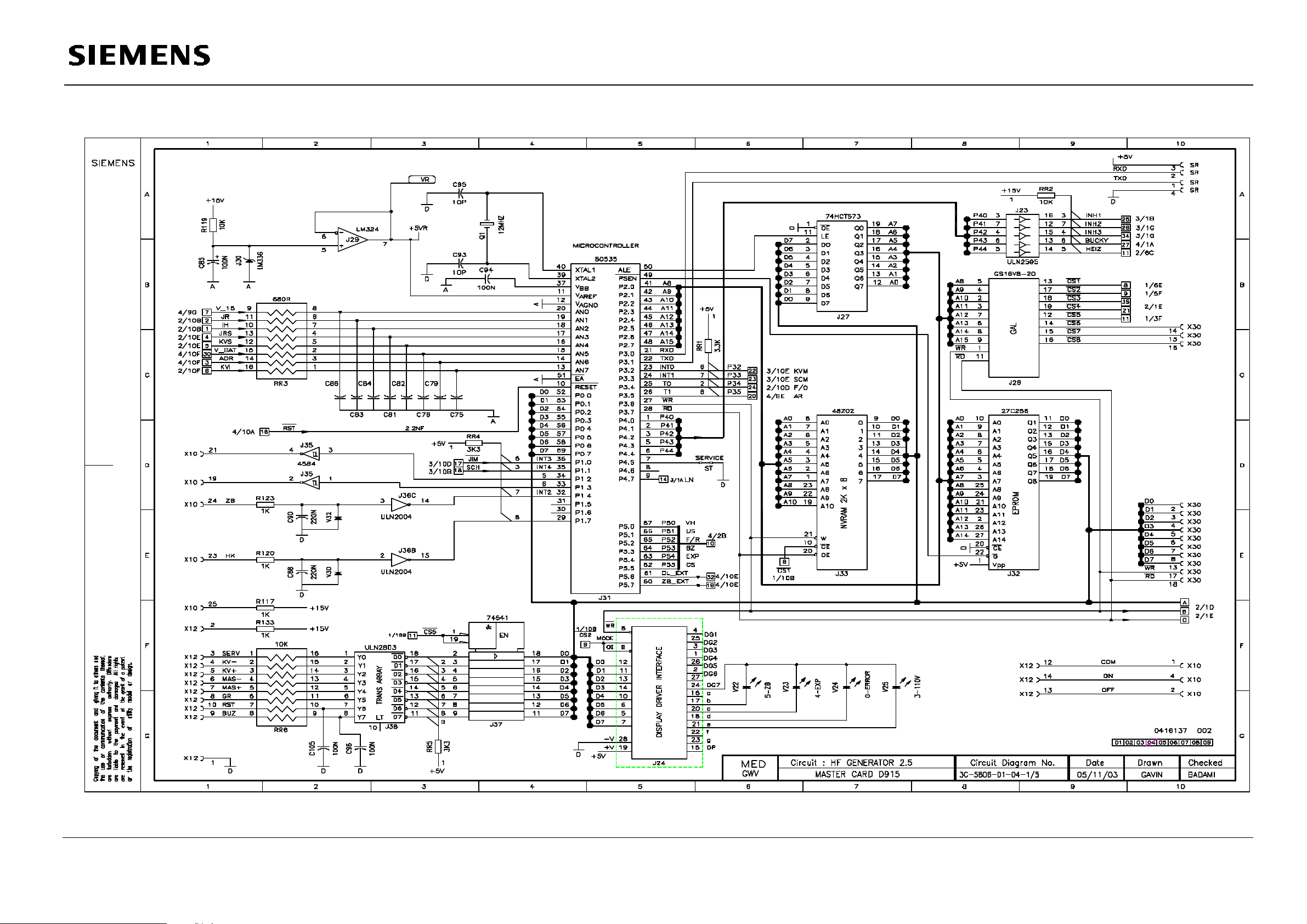
5 Circuit Diagrams
SIEMENS
H F GENERATOR
Service Manual
Circuit Diagrams
I N D E X
SR. NO. DRG. NO.
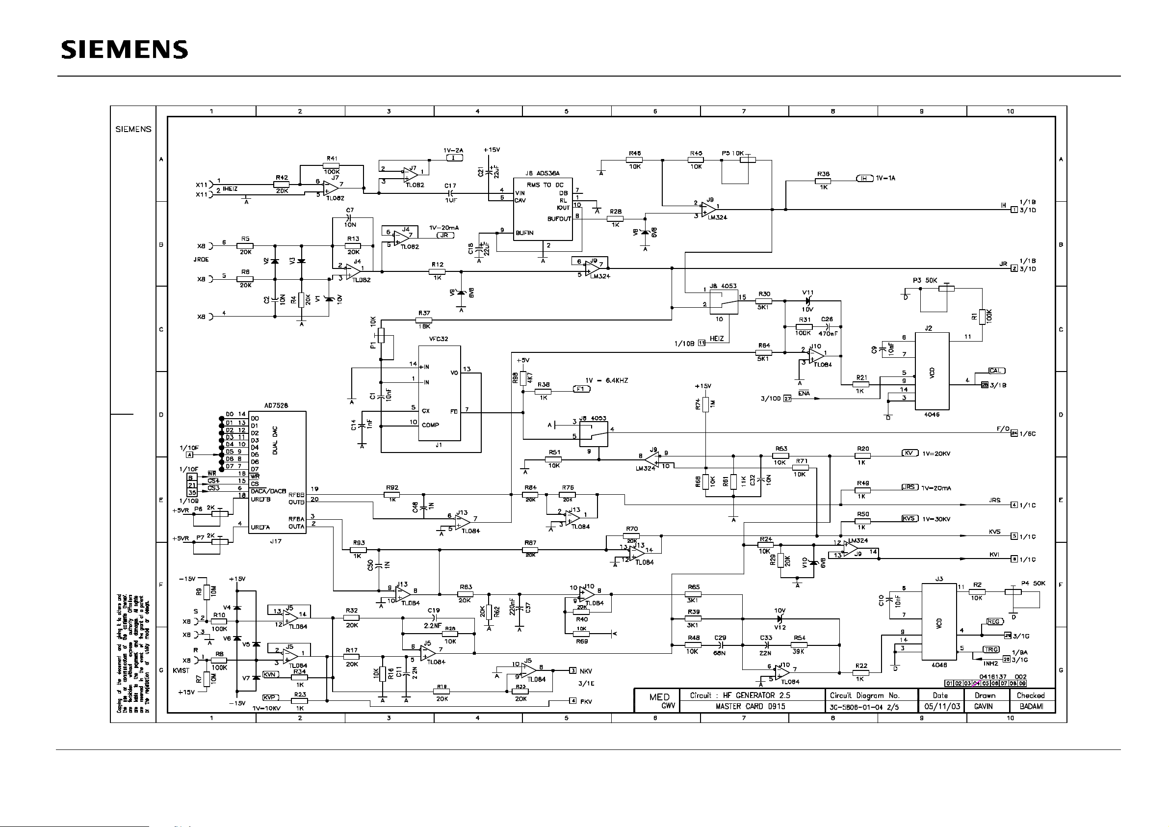
3C-5806-01-04 MASTER CARD D915
1.
2.
3C-5806-03-02 INTERFACE CARD D920
3.
3C-5806-04-01 MAIN INVERTER D61
4.
3C-5455-08-01 DISPLAY PCB D932
5.
4C-5455-09-02 KEY PCB D936
6. 1
4C-5206-01-01 D1 TIMER PCB
DESCRIPTION
NO. OF PAGES
5
2
1
1
1
Circuit: Circuit Diagram Date Drawn Checked
Copying of the document and giving it to others and
the use or communication of the contents thereof,
are forbidden without express authority. Offenders
Siemens Ltd. Med India Version 6.0
MED
are liable to the payment and damages. All rights
are reserved in the event of the grant of a patent
or the registration of utility model or design.
GWV
INDEX
4C-5806-03 1/1 GAVIN
Copyright SIEMENS LTD. All rights reserved. For internal use only
05/11/03 BADAMI
5-4
Page 6
Service Manual
Circuit Diagrams
Siemens Ltd. Med India Version 6.0
Copyright SIEMENS LTD. All rights reserved. For internal use only
5-5
Page 7
Service Manual
Circuit Diagrams
Siemens Ltd. Med India Version 6.0
Copyright SIEMENS LTD. All rights reserved. For internal use only
5-6
Page 8

Service Manual
Circuit Diagrams
Siemens Ltd. Med India Version 6.0
Copyright SIEMENS LTD. All rights reserved. For internal use only
5-7
Page 9

Service Manual
Circuit Diagrams
Siemens Ltd. Med India Version 6.0
Copyright SIEMENS LTD. All rights reserved. For internal use only
5-8
Page 10

Service Manual
Circuit Diagrams
Siemens Ltd. Med India Version 6.0
Copyright SIEMENS LTD. All rights reserved. For internal use only
5-9
Page 11

Service Manual
Circuit Diagrams
Siemens Ltd. Med India Version 6.0
Copyright SIEMENS LTD. All rights reserved. For internal use only
5-10
Page 12

Service Manual
Circuit Diagrams
Siemens Ltd. Med India Version 6.0
Copyright SIEMENS LTD. All rights reserved. For internal use only
5-11
Page 13

Service Manual
Circuit Diagrams
Siemens Ltd. Med India Version 6.0
Copyright SIEMENS LTD. All rights reserved. For internal use only
5-12
Page 14

Service Manual
Circuit Diagrams
Siemens Ltd. Med India Version 6.0
Copyright SIEMENS LTD. All rights reserved. For internal use only
5-13
Page 15

X4
X4
7
V24
8
F5 4A
1 2
R38
X11
X11
X11
10K
15
V25
13
16
R31
560R
1
2
V18
2 1
~
~
3
4N35
6
J7
4
+
-
5
4
R32
100K
+
-
C14-17
2200µF
0.1µF
C20
NTC
R22
5.6K
2.5R
C11
2.7K
R26
0.1µF
R37
1K
R23
1K
R25
560R
V21
2N2222A
2N6107
V19
2N3055
C12
1nF
V20
R24
100R
R33
100K
V26
V27
R27
0.1R
R34
100K
100K
R36
+
3
-
2
100K
mA+ mA-
R35
V22
5.6V
mAS
Service Manual
Circuit Diagrams
2
100K
3
R100
1
4
100K
R101
VH+
11
R28
R29
K5
C13
13 13 9
100R
100R
0.33µF
K5
R30
1K
X11
1
X20
1
X11
11
X20
3
X2
X2
5
X8
4
6
X8
X8
5
X2
4
+24V
240/264V~
24/29V~
240/264V~
+24V
240/264V~
0VL
X2
X2
1
2 2
K4
4
8
9
13 3, 5
K4
2, 4
9
GA
GA
16
3, 5
1
2.4
GA
GB
GA
1
GB
10
GB
GA
GB
9
GB
16
GB
1
X8
X8
3
X8
X10
X10
X10
X20
18
X20
11
X11
12
+15V
100K
3.3K
100K
100K
3.3K
100K
100K
3.3K
100K
24 G1/G2
11
GA
12
GA
13
GA
240 G1/G2
11
GB
12
GB
13
GB
X10
K4
5
4
0VL
+24V
1
16
V16
IN4007
8
X10
+15V
R21
1K
4N35
3
1
2
J5
+15V
DL_RELVH_REL
4N35
1 5
2
J6
HCPL3700
R6
4.7K
R7 4.7K
R8 4.7K
3
5
0.1µF
0.1µF
0.1µF
C4
C5
15
16
C6
0VD
8
J2
6
5
HCPL3700
8
J3
6
5 4
HCPL3700
8
J4
6
5
1
2
+
3
4
1
2
+
47µF
3
1
2
+
47µF
3
4
C7
C8
C9
47µF
0VL
AR
ZB-EXT
DL-EXT
8.2K
R9
8.2K
R10
8.2K
R11
R12
R13
R14
R15
R16
R17
R18
R19
R20
X11
14
X11
+24V
1
K5
16
4
0VL
V17
IN4007
Siemens Ltd. Med India Version 6.0
Copyright SIEMENS LTD. All rights reserved. For internal use only
5-14
Page 16

Service Manual
Circuit Diagrams
Siemens Ltd. Med India Version 6.0
Copyright SIEMENS LTD. All rights reserved. For internal use only
5-15
Page 17

Service Manual
Circuit Diagrams
X1.10
LN
X4.1
X4.2
X4.3
X4.4
X4.5
X1.1
X1.2
X1.3
X1.4
X1.5
X1.6
X1.7
X1.8
X1.9
K2
JMP1
JMP2
5
7
V1
V3
K3 K5
240V
1
3
2
269V
24V
1
3
2
29V
F1
250mA
R1
100K
IN4007
4
4
8
8
630mA
1 2
630mA
1
T1
V9
V9
V23
8
6
+
~
~
-
R3
10K
V10
IN4007
V12
21
V2
IN4007
4
8
2
V7
IN4007
V8
IN4007 IN4007
K6
100K
1
4
R2
V13
IN4007
V11
C1
R46
100K
P1
100K
240/264V~
24/29V~
+
-
+
-
1000µF
V33
+24V~
C2
100µF
0VL
J10
1 3
7812
2
C18
0.1µF
100K
R44
V28
100K
R45
V29
100K
R43
10µF
+
-
C19
5
6
V30
IN4007
K1 1
16
J8
100K
R42
2 ZB
4 6
V4
IN4007
K1
K2
K2
1
V5
2
4
COM
X10
2
X10
1
X10
6
5
X11.2
7
X10.17
X27
3 HK
X27
1 COM 25
X27
1 +15V
X3
2 DEV-BUCKY
X3
3 DEV-EXP
X3
4 DEV-CS
X3
14 DISP 1
X20
13 DISP 2
X20
16 SCH
X20
1K
20 VP 1
X20
X20
X20
X20
X20
15
13
17
10
0VL
1
16
5
4
+24V
K6
LN_REL
4N35
J9
+15V
R50
1K
1
X11.7
2
R39
24
X10
23
X10
X10
13
X10
14
X10
7
X20
10
X10
6
X10
4
X6
3
X6
2
X6
X6
6
X6
5
X6
8
X6
9
X6
X12A
X12A
EARTH
10A
2
R4
10K
V15
V14
1
1
2
1
2
X12B
X12B
V6
IN4007
0VL
16
1
+24V
K3
5
4
US_REL
4N35
6
J1
+15V
1
12
2
X10
F4
Siemens Ltd. Med India Version 6.0
Copyright SIEMENS LTD. All rights reserved. For internal use only
X10
X10
X10
X10
5
7
9
10µF
+
C3
-
+15V
0VD
11
5-16
Page 18

Service Manual
Circuit Diagrams
Siemens Ltd. Med India Version 6.0
Copyright SIEMENS LTD. All rights reserved. For internal use only
5-17
Page 19

Service Manual
Circuit Diagrams
Siemens Ltd. Med India Version 6.0
Copyright SIEMENS LTD. All rights reserved. For internal use only
5-18
Page 20

SIEMENS
Service Manual
Circuit Diagrams
X12
X12
X12
X12
X12
X12
X12
X12
X12
1 COM
3 DL_SERV
6 KV+ / (mAs - *)
7 KV- / ( mAs + *)
4 mAS+ / (KV- *)
5 mAS- / (KV+ *)
12 COM
14
ON
001
002*
001
13
OFF
002*
S5
S2
S1
S4
S3
S7
S6
I / ( 0*)
0 / ( I*)
1
X36
8 GR
X12
10 RESET
X12
9 BUZ
X12
1
X1
V1
2
Circuit: Date
MED
or the registration of utility model or design.
are reserved in the event of the grant of a patent
are liable to the payment and damages. All rights
are forbidden without express authority. Offenders
the use or communication of the contents thereof,
Copying of the document and giving it to others and
Siemens Ltd. Med India Version 6.0
GWV KEY PCB D936
Circuit Diagram
4C-5455-09-02 1/1
3
4
5
GAVIN
X36
X36
X36
CheckedDrawn
BADAMI
5-19
Copyright SIEMENS LTD. All rights reserved. For internal use only
Page 21

SIEMENS
Service Manual
Circuit Diagrams
500K
LAMP
100K
C1
1000µF
0V
680R
680R
10nF
1N4007
40V
Copying of the document and giving it to others and
Siemens Ltd. Med India Version 6.0
GWV
Copyright SIEMENS LTD. All rights reserved. For internal use only
4C 5206 - 01 - 01
Circuit: DateCircuit Diagram CheckedDrawn
MED
or the registration of utility model or design.
are reserved in the event of the grant of a patent
are liable to the payment and damages. All rights
are forbidden without express authority. Offenders
the use or communication of the contents thereof,
5-20
 Loading...