

Page 1

MULTIMOBIL 2.5
Function Description
SP
© Siemens AG 2003
The reproduction, transmission or
use of this document or its contents
is not permitted without express
written authority. Offenders will be
liable for damages. All rights,
including rights created by patent
grant or registration of a utility
model _or_ design,_are_ reserved.
English
Print No.: SPR8-X01.850.01.02.02 Doc. Gen. Date: 09.05
Replaces: SPR8-X01.850.01.01.02
Page 2
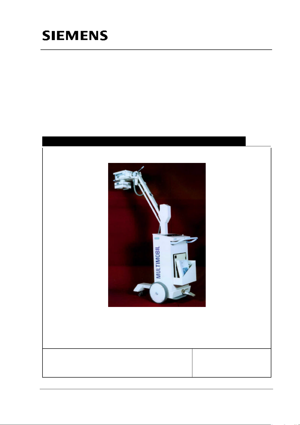
Multimobil 2.5
Service Manual
Circuit Description
Med
Circuit Description
Version: 6.0
Copyright SIEMENS LTD.,MED INDIA
Siemens Ltd. Med India Version 6.0
Copyright SIEMENS LTD. All rights reserved. For internal use only
The reproduction, transmission or use of
this document or its contents is not
permitted without express written
authority. Offenders will be liable for
damages.
6-1
Page 3

Service Manual
Circuit Description
INDEX
6 CIRCUIT DESCRIPTION ...................................................................................................6-3
6.1 MASTER CARD D915 .......................................................................................................6-3
6.1.1 Power Supply........................................................................................................6-3
6.1.2 RESET Generation................................................................................................6-3
6.1.3 Crystal Operation ..................................................................................................6-3
6.1.4 Microcontroller ......................................................................................................6-3
6.1.5 Octal Latch...........................................................................................................6-3
6.1.6 GAL.....................................................................................................................6-3
6.1.7 EPROM................................................................................................................6-4
6.1.8 NVRAM................................................................................................................6-4
6.1.9 Serial Communication............................................................................................6-4
6.1.10 Keyboard..............................................................................................................6-4
6.1.11 Display.................................................................................................................6-4
6.1.12 kVsoll and mAsoll .................................................................................................6-4
6.1.13 Line voltage monitoring..........................................................................................6-4
6.1.14 kV Feedback .......................................................................................................6-5
6.1.15 IH Feedback ........................................................................................................6-5
6.1.16 mA Feedback .......................................................................................................6-5
6.1.17 kV Regulation .......................................................................................................6-5
6.1.18 Filament Regulation...............................................................................................6-6
6.1.19 mAs Integration ....................................................................................................6-6
6.1.20 Control of the Firing Pulse Frequencies REG and CAL.............................................6-6
6.1.21 Generation of actual Firing Signals .........................................................................6-6
6.1.22 kVmax, mAmax Feedback ....................................................................................6-7
6.2 IGBT INVERTER ASSEMBLY D61..........................................................................................6-7
6.2.1 Firing ...................................................................................................................6-7
6.2.2 Inverter.................................................................................................................6-8
6.2.3 SCM ....................................................................................................................6-9
6.3 INTERFACE PCB D920 ................................................................................................... 6-10
6.3.1 ON/OFF Circuit ................................................................................................... 6-10
6.3.2 Line voltage measurement ................................................................................... 6-10
6.3.3 Power Supply Distribution .................................................................................... 6-10
6.3.4 Filament Circuit................................................................................................... 6-11
6.3.5 Filament Supply and Heating ................................................................................ 6-11
6.3.6 Stand-by State.................................................................................................... 6-11
6.3.7 Preparation State ................................................................................................ 6-11
6.3.8 Filament Current Feed Back ................................................................................ 6-11
6.3.9 Tube Current Feedback ....................................................................................... 6-12
6.3.10 Collimator Supply ................................................................................................ 6-12
6.4 KEYBOARD PCB D936 .................................................................................................. 6-12
6.4.1 Keypad............................................................................................................... 6-12
6.4.2 Interface with Master Card.................................................................................... 6-12
6.5 DISPLAY PCB D932 ...................................................................................................... 6-13
6.5.1 Connections ....................................................................................................... 6-13
6.5.2 Interface with Master Card.................................................................................... 6-13
6.6 SWITCH MODE POWER SUPPLY 40 WATTS.......................................................................... 6-13
6.6.1 Specifications..................................................................................................... 6-13
6.7 SWITCH MODE POWER SUPPLY 120 WATTS........................................................................ 6-14
6.7.1 Specifications..................................................................................................... 6-14
Error! No index entries found.
Siemens Ltd. Med India Version 6.0
6-2
Copyright SIEMENS LTD. All rights reserved. For internal use only
Page 4

Service Manual
Circuit Description
6 Circuit Description
6.1 Master Card D915
6.1.1 Power Supply
The +15, 0V, -15V and +5V, 0V voltages are obtained from the SMPS through the
connector X15.
The reference voltage for the Microcontroller (J31) is 5V and it is generated by R119,
C85, and J30.
6.1.2 RESET Generation
The RST signal is generated by IC J40 (MAX700 : power supply monitor with reset)
at power ON. The switch SW2 also allows for manual reset of the system.
On actuating SW2 ON, reset is generated by J40 which is applied to RST of J31.
6.1.3 Crystal Operation
The 12 MHz Quartz crystal forms a Pierce Oscillator along with the two capacitors
C93 and C95. The output of the oscillator is a 12MHz sinusoidal wave which is
applied to XTAL1 and XTAL2 inputs of J31 for providing timings for internal operations
of the microcontroller.
6.1.4 Microcontroller
The microcontroller J31 outputs multiplexed lower order address bus and the data bus
on port ‘P0’ and higher order address bus on port ‘P2’.
The control signal RD, WR along with A8-A15 are provided to J28 (GAL) to generate
the chip select signals for accessing various peripherals.
The status signal PSENis used for reading external program stored in EPROM J32.
The EA ‘LOW’ allows accessing the external program memory.
Different signals for controlling various operations of the entire system are provided by
the Microcontroller on its ports P1, P3, P4, P5.
The analog inputs AN0 - AN6 are used for monitoring analog signals.
The pins TxD and RxD are used for serial communication between the processor and
the external device such as a Computer for servicing.
The Service switch ST provided at pin P4.5 is used for operating the Unit in the service
mode.
6.1.5 Octal Latch
The multiplexed address and the data bus is separated by the octal latch J27.
At the active ALE signal, the lower order address (A0-A7) is latched.
6.1.6 GAL
Since Memory mapping technique is used, the chip select signals for various
peripheral devices are generated by the Gated Array Logic IC J28. The inputs are the
Siemens Ltd. Med India Version 6.0
Copyright SIEMENS LTD. All rights reserved. For internal use only
6-3
Page 5

Service Manual
Circuit Description
address lines (A8 - A15), and the control signals RD and WR. The output lines are
CS1 to CS8.
These output chip select lines are generated on the basis of the logic implemented in
the program stored in the GAL.
6.1.7 EPROM
The entire program is stored in a single EPROM J32.
6.1.8 NVRAM
The 2 Kbyte NVRAM stores the variables during the opertion of the unit.
A0 - A10 and D0 - D7 are the address and the data lines provided to the RAM. The
first 2K bytes of entire memory space 0000H to 07FFH is used as RAM.
6.1.9 Serial Communication
TxD, RxD are provided to the serial communication port of D915. Various activities of
the unit can be controlled by an external device such as a PC. The serial port is meant
for testing and service purposes.
6.1.10 Keyboard
The keys are accepted through X12 from D936.
The keys kV+ , kV -, mAS+, mAS- are accepted on the data bus through J38 and J37
at the address 9000H.
The ON, OFF signals are routed via X12, D915, X10 to D920.
6.1.11 Display
The data bus, the control signal WR and the chip select signal CS2 are provided to
the Display Driver J24 on D932 through X1. Writing the control word and the string of
8 byte data at the addresses 8000H and 8800H respectively displays the kV and mAS
values and lights up function related LEDs on D915.
6.1.12 kVsoll and mAsoll
The kVsoll and mAsoll values are generated by Dual Digital to Analog Converter J17
and the Opamp J13 acting as I - V converter.
The microcontroller J31 outputs the digital values of kVsoll and mAsoll on the data bus
at address A000H (CS3) and A100H ( CS4) respectively. The reference current for
DAC is adjusted by means of presets P6 and P7.
The kVsoll and mAsoll are fed back to the AN3 and AN4 pins of J31 for ensuring their
proper values. These soll values are also used for regulation of kV and mA.
The kV soll ratio is 1 V = 30 kV and the mAsoll ratio is 1 V = 20 mA.
6.1.13 Line voltage monitoring
The actual mains Line voltage stepped down & converted to DC and through
differential amplifier it is fed to V-Bat input point of ADC . This DC voltage is
monitored every 5 second in standby mode of unit and line voltage is displayed
Siemens Ltd. Med India Version 6.0
Copyright SIEMENS LTD. All rights reserved. For internal use only
6-4
Page 6

Service Manual
Circuit Description
during first step of hand release switch for radiography. If the measured Line voltage is
less than 200 volts , microcontroller sends one signal to switch ON the LN contactor
which will support extra voltage through auto transformer for 2.5 KW power generation.
This switching ON/OFF of LN contactor is done every 5 sec in standby mode of unit. In
preperation and exposure mode contactor retains its position. After 5 second of each
termination of radiography Line voltage is monitored once again.
6.1.14 kV Feedback
The actual kVp across the tube is stepped down and fed back to the Master card
D915 at pins 1, of X8 as PKV with respect to the common terminal at pin 3.
PKV is passed through the voltage follower J5 and then fed to the Differenial
Amplifier formed by J5 to produce kVist used for kV regulation.
(kVist ratio is 1V= 20 kV)
As no differntial configuration is used, NKV part is ignored by grounding it.
kVist is fed back to AN7of J31 for monitoring purpose.
6.1.15 IH Feedback
The filament current feedback is taken from the Interface card D920 through X11.1.
J7 provides a gain of 5 to Ih.
The AC filament current Iheiz is converted in DC value Ih by RMS-DC converter J6.
J9 provides an approprate gain to Ih (that can be adjusted by preset P5) so that the
ratio 1V = 1A holds true. Ih is fed back to J31 at AN2 for monitoring purpose and the
same is used for Ih regulation.
6.1.16 mA Feedback
The tube current (JR) is fed back at pin 5 of X8 on D915 & is applied to the
Differential Amplifer formed by J4.
The output JR represents the actual tube current mAist which is fed back to J31 at AN1
through J9 for monitoring purpose. JR is also used for tube current regulation.
6.1.17 kV Regulation
The kVsoll and kVist values are fed to the P-I controller formed by IC J10.
The difference between the kVist and kVsoll value is amplified to produce an
appropriate error output, so as to compensate the error. The zener V12 limits the
maximum output voltage of the error amplifier to 10V.
The error amplifier output is fed to PLL IC J3 which is used as voltage to frequency
converter. The J10 output voltage produces an equivalent frequency REG at J3 output.
For 10V, REG (the maximum firing frequency of the Main Inverter) is approx. 9.2 kHz.
J3 is enabled by an active low INH2 signal provided by the microcontroller J31 at P4.1
through J23. During HT, J3 is enabled through INH2 and J3 results in a firing frequency
of Main Inverter Igbt‘s, to result in actual kV in line with the required value.
Siemens Ltd. Med India Version 6.0
Copyright SIEMENS LTD. All rights reserved. For internal use only
6-5
Page 7

Service Manual
Circuit Description
6.1.18 Filament Regulation
Filament Regulation is divided into two parts:
1. Regultion without high voltage : The filament current Ih is regulated. CPU J31
feeds the required filament current value to the input of DAC.
2. The actual tube current JR is regulated. J31 outputs the required tube current on the
input of DAC. Depending upon whether the regulation is pre H.T or post H.T either Ih or
JR is selected through HEIZ signal from J31 (P4.4) and used for regulation together
with the corresponding value from the DAC. The output of the error amplifier J10 is fed
to PLL J2 which is configured as voltage to frequency converter. The PLL J2 is
enabled through INH1 signal from J31(P5.0) and generates a frequency in line with the
output of error amplifier J10 to result in required filament current or the tube current.
6.1.19 mAs Integration
The actual tube current is applied to the input of V-F converter J1. The transfer ratio (
Frequency to Voltage) of J1 is adjusted by preset P1. The output frequency is
selected by J8 only when the kVist reaches 64% of its final value.
The output of J8 is fed to J31 as timer 0 clock .The timer 0 inside J31 is configured as
timer counter which is preloaded with a count equivalent to mAs value.The incoming
clock decrements the counter and on reaching ‘0’, generates an interrupt to terminate
the exposure.
6.1.20 Control of the Firing Pulse Frequencies REG and CAL
REG is controlled by the signals INH2 and INH3 and it is enabled only when
INH2=0 and INH3 =1 .
CAL is enabled only when INH1=0.
6.1.21 Generation of actual Firing Signals
6.1.21.1 Main Inverter Firing Frequency
The pulse duration of the actual firing signals of the Main Inverter is decided by the
Monoshot Multivibrator J21 (IC 4538 Dual Monoshot Multivibrator) and R104, C66 and
R105, C67.
The RST pin of J21 is normally high for its proper operation.
The outputs of J21 at pins 6 and 10 are out of phase. These signals are optically
isolated by J39 and J41 and fed to the Main Inverter Driver (D61) through X20.14 and
X20.18 .
6.1.21.2 Filament Regulator Firing Frequency
J18 is used to determine the pulse width of the the actual firing signals of the Filament
Regulator. The IC J20 ensures that the firing pulses to the Filament regulator are out of
phase. These signals are inverted by J22 and fed to the Filament regulator firing circuit
on D915 through X11.13 and X11.16.
Siemens Ltd. Med India Version 6.0
Copyright SIEMENS LTD. All rights reserved. For internal use only
6-6
Page 8

Service Manual
Circuit Description
6.1.21.3 Main Inverter Short Circuit Feedback SCM
During normal operation, the transistor V39 is ON and simultaneously the optocoupler
is also ON. An active LOW error signal at X20.16 turns V39 and consequently J34
OFF. The J34 output becomes LOW to give the HIGH SCM (Main Inverter short circuit)
signal. SCM is inverted by J22 and then it is fed back to the microcontroller J31 for
taking the corrective action.
The three signals SCM , KVM and JIM are used for disabling the Driving pulses of the
Main Inverter. This is done by ORing of these three signals by J14. At the occurrence
of either of these three signals, RST goes LOW and its output is disabled.
6.1.22 kVmax, mAmax Feedback
6.1.22.1 KVM maximum kV
If the KVP value exceeds the reference value for 110kV at J12 (Comparator)
its output generates the KVM signal. KVM is also fed back to J31 at P32 as T0
Interrupt for initiating necessary corrective action like stopping the exposure
instantaneously.
6.1.22.2 JIM maximum mA
An increase in Ih or JR than the reference values of 4.4A and 71 mA respectively
generates JIM. JIM is fed as T1 interrupt to J31.
6.1.22.3 IH Maximum
This error is similar to JIM. This is monitored during standby and preparation state and
gives an interrupt if the filament current exceeds the maximum permissible current that
is 4.2 Amperes.
6.2 Igbt Inverter Assembly D61
Igbt Inverter Assembly houses Igbt’s configured as bridge inverter, along with Inverter
Pcb D61 consisting of associated firing circuit, supply monitoring and short circuit
sensing circuit.
6.2.1 Firing
With second step of exposure release switch pressed, the microcontroller prepares for
the exposure loading the kV and mA values required for the exposure into the DAC.
This control circuit residing on the Master Card D915 then generates the firing pulses
for the inverter which are available at the connector X6 of the inverter PCB through
interface PCB D920.
On Inverter PCB D61, J1 along with resistors R13, R14 and capacitors C5, C6 form
the pulse stretching circuit which stretch the Disp1 and Disp2 pulses to 64 µ Sec
(the resonating time of the LC load) maintaining 180° phase shift. These phase shifted
pulses drive the Igbt drivers which in turn generate the gate firing pulses for the Igbt’s.
Siemens Ltd. Med India Version 6.0
Copyright SIEMENS LTD. All rights reserved. For internal use only
6-7
Page 9

Service Manual
Disp 1
Circuit Description
Resistors R1, R4, R7, R10 control the turn-on speed of the Igbt’s. Resistors R2, R5,
R8, R11 control the turn-off speed of the Igbt’s.
6.2.2 Inverter
U/V is the primary widing of the HT trafo which is in series with external resonating
capacitor C4 and external inductor L2.
With Disp1 pulse the current path is completed through DC(+), 3-1 of IG1, A3, U/V, C4,
L2, A2, 1-2 of IG2, DC(-). After 64 µ Sec the gate pulse is turned off and the Igbt’s are
turned off. The resonating capacitor C4 which is now charged to a voltage greater than
the bank voltage discharges via the free-wheeling diodes in anti-parallel to the Igbt’s.
The Waveforms for the energy packet flowing through the primary winding can be
measured by connecting a current transformer across A3 or A2 .The waveform for the
the same when Disp 1 is present is shown below.The turns ratio of the current
tranformer used is 1000:1 with a 100 resistor across the
secondary.
Resonant
energy
packet
With Disp2 pulse the current path is completed through DC(+), 3-1 of IG2, A2, L2, C4,
U/V, A3, 1-2 of IG1, DC(-). After 64 µ Sec the gate pulse is turned off and the Igbt’s are
turned off. The resonating capacitor C4 which is again charged to a voltage greater
than the bank voltage discharges via the free-wheeling diodes.
The waveform for the energy packet flowing through the primary winding when Disp 2
is present is shown below.The turns ratio of the current tranformer used is 1000:1 with
a 100 resistor across the secondary.
Siemens Ltd. Med India Version 6.0
Copyright SIEMENS LTD. All rights reserved. For internal use only
6-8
Page 10

Disp 2
Service Manual
Circuit Description
Resonant energy packet
The resonant period for either pair of IGBT’s firing should be between 64-72µ Sec and
the peak to current should be approximately 125 Amps .
The firing pulses have a maximum frequency of 9.2 kHz ± 0.3kHz.
The presence of DC voltage is indicated by LED V1 on D61.
6.2.3 SCM
VCE of the Igbt is monitored continuously by the Igbt drivers. In case of short in any
Igbt’s VCE will increase resulting in generating of active low signal on ERR pin of the
driver. ERR pin is normally held high by a pull-up resistor in D920. The ERR pin can go
low if the supply voltage falls below 13V instead of 15V. When this signal is sensed by
the microcontroller, firing pulses are inhibited and Error Code 11 is displayed, and the
IGBT’s are turned off.
Siemens Ltd. Med India Version 6.0
Copyright SIEMENS LTD. All rights reserved. For internal use only
6-9
Page 11

Service Manual
Circuit Description
6.3 Interface PCB D920
6.3.1 ON/OFF Circuit
The mains voltage of 240 V ac appears across X1.1 and X1.2. The 15 Volts
transformer T1 and regulator 7812 on the PCB provides the coil voltages for the On /
Off relays K2 & K1. When Unit On switch is pressed, the circuit for Relay Coil K2
gets completed and causes the Relay K2 to energise. This causes the contact (5,7) of
K2 to close which will provide the AC voltage to circuit points like SMPS (40 watts
&120 watts) input and Contactor Coil connections it also causes contactor CS to pick
up and provide the direct Line voltage to the Main Transformer T1 and to the full wave
rectifier for charging the capacitor bank via the 47Ù parallel resistance. As the coil K2
energises the contact K2 (6,5) is establised and hence the unit remains On even if the
switch is released.
When the switch is pressed, the Relay K1 coil is energised and this causes the
Normally Closed contact K1 (4,6) of relay K1 to open thereby opening the circuit
connections for relay K2. The Unit thus is turned Off.
6.3.2 Line voltage measurement
Incomming Line voltage is stepped down to 15 volts when input is 230 AC. It is
converted to DC & filtered using capacitor. This DC voltage is further stepped down
using resistor divider network and given to differential amplifier for line voltage
measurement through ADC on Master card D915.
6.3.3 Power Supply Distribution
The following connections are routed through the Interface PCB D920.
1. X1.9 & mains neutral 240 V ac for Contactor US Coil Connections
2. X1.4 & X1.6 240 V ac for SMPS (40 watts) input supply
3. X1.5 & mains neutral 240 V ac for CS Contactor coil connections
4. LN on D920 & mains neutral 240 V ac for Contactor LN Coil Connections
5. X1.8 & mains neutral 240 V ac for SMPS (120 watts) input supply
The contactor US and LN coils are energised only when corresponding signal from the
Master Card D915 is obtained. This is achieved through optocouplers J1 and J9
respectively. The contactor On signal from the Master Card D915 inturn drives
optocoupler J1 / J9 which in turn K3 / K6 relay to connect the 240 V ac to the coil.
Siemens Ltd. Med India Version 6.0
Copyright SIEMENS LTD. All rights reserved. For internal use only
6-10
Page 12

Service Manual
Circuit Description
6.3.4 Filament Circuit
The interface for the filament is built in a series regulator form. The filament is driven for
the required heating i.e. of the predetermined value of current through an arragement
of controller, driver circuit and final regulator circuit. Out of these three the controller
circuit exists on the Master Card D915. The driver part J7 and the series regulator are
formed on the Interface PCB D920.
6.3.5 Filament Supply and Heating
The DC supply of around 24 volts is obtained by SMPS 120 watts.This is then passed
through bridge rectifier to avoid wrong connections of positive and negative terminals
of SMPS & filtered to obtain a smooth DC by a bank of four 2200µF capacitors. The
Bank of capacitors help in reducing the heavy current spikes that might result if a single
capacitor of a large value is used. The collector voltage to V20 transistor is given
through NTC 2.5R to reduce inrush filament current. The firing Pulses for the driver
optocoupler J7 are the Drive1 and Drive2 pulses added together. These pulses switch
the driving transistor for the regulator 2N2222. In this manner the Power transistor
2N3055 V20 is operated in the switching mode to obtain the pulsating DC for the
filament heating.
6.3.6 Stand-by State
In the standby state of the system the filament is heated to 2 Amp. This value is
decided on the basis that heating is below radiation value and sufficient enough to
allow the radiation within 1.2 seconds of preheating.
6.3.7 Preparation State
This is entered when the exposure release switch is pressed half-way to make only first
step contact. In this state the filament is boosted to get heated to a value so that the
required mA (Tube Current) is achieved under exposure condition.
The maximum value of boosting current is restricted to 4.2 Amperes.
6.3.8 Filament Current Feed Back
The control circuit on the Master Card D915 receives the feedback voltage
corresponding to the actual filament current inorder to achieve the filament current
regulation during standby and boosting states and Tube Current / mA regulation in
case of exposure state. For this purpose one 0.1 Ω resistor is introduced in series with
the filament. This gives current to voltage converstion with the conversion factor of 100
mv = 1 A. This in turn is differentially amplified by the IC J8 to give the final current ratio
of 1 V = 2 A.
Siemens Ltd. Med India Version 6.0
Copyright SIEMENS LTD. All rights reserved. For internal use only
6-11
Page 13

Service Manual
Circuit Description
6.3.9 Tube Current Feedback
Similar to Filament current feedback the tube current feedback is taken from the Single
Tank is available at X2.4, X2.5. The combinition of 100 Ù reistances in parallel give
the tube current ratio of 1 V = 20 mA.
6.3.10 Collimator Supply
The collimator supply of 12 V ac is obtained from the mains Transformer and is made
available on X12 connections after introducing a LED indicator and a 10 A protecting
fuse.
6.4 Keyboard PCB D936
6.4.1 Keypad
No. Identification Description Hex Code
1
Unit OFF n.a.
2
Unit On n.a.
3 kV + kV increment F7
4 kV - kV decrement EF
5 mAs + mAs increment FD
6 mAs - mAs decrement FB
7 DL_Serv Service mode select FE
6.4.2 Interface with Master Card
The keyboard switches are connected to the Master Card D915 through X12
connector. The switch action is conveyed to the Master Card by a switching 15 Volts
signal. In normal condition when no key is pressed all the key lines are maintained at
LOW. This in turn is reflected at the port 9000H as all high as FFH.
Whenever a key is depressed, it is connected to the 15 V dc line and the
corresponding line on the port 9000H goes low. Thus the cooresponding data code
appears on the Data bus of the Microcontroller which is then read by the controller
through the READ$KEYB routine.
Siemens Ltd. Med India Version 6.0
Copyright SIEMENS LTD. All rights reserved. For internal use only
6-12
Page 14

Service Manual
Circuit Description
6.5 Display PCB D932
6.5.1 Connections
The display PCB consists of a Display Driver IC 7218B and the seven segment
displays. The Display driver is mapped at address 8000H. Thus it is configured to
receive the Code at 8000H and the data values from 8800H.
The data segments are configured as…
1. mAs Unit
2. mAs tens
3. mAs Hundreds
4. kV Unit
5. kV Tens
6. kV Hundreds
The same data locations are used for error code display also. In such case the Error
code is displayed.
6.5.2 Interface with Master Card
The connection for the display card is obtained by 28 pin Flat Band DIP connector
which carries the necessary signals for the IC 7218 from Master card to Display PCB.
The Eighth line of the controller is used for error LED Displays on the Master Card.
6.6 Switch Mode Power Supply 40 watts
6.6.1 Specifications
The Switch mode power supply is used to supply + 5 Volts to the controller and
associated circuitry and ± 15 V to the driver circuits.
The following are the specifications of the supplies.
+ 5 V at 3 Amps with Tolerance of 3%
+ 15 V at 0.3 Amps with Tolerance of 10 %
- 15 V at 0.2 Amps with Tolerance of 5 %
This output is maintained for the following range of the input conditions.
180 V ac to 260 V ac at 50 Hz ± 5 Hz and an input current of 0.7 Amp rms.
All out puts are protected for short circuit conditions and a sharp repeatitive sound is
heard from the SMPS in the event of short circuit. The circuit behaves normally upon
the removal of the short circuit.
Siemens Ltd. Med India Version 6.0
Copyright SIEMENS LTD. All rights reserved. For internal use only
6-13
Page 15

Service Manual
Circuit Description
6.7 Switch Mode Power Supply 120 watts
6.7.1 Specifications
The Switch mode power supply is used to supply + 24 Volts to the Filament and
associated circuitry.
The following are the specifications of the supplies.
+ 24 V at 5 Amps with Tolerance of 3%
This output is maintained for the following range of the input conditions.
160 V ac to 265 V ac at 50 Hz ± 5 Hz and an input current of 0.7 Amp rms.
All outputs are protected for short circuit conditions. The circuit behaves normally upon
the removal of the short circuit.
Siemens Ltd. Med India Version 6.0
Copyright SIEMENS LTD. All rights reserved. For internal use only
6-14
 Loading...