

Page 1

MULTIMOBIL 10
Function Description
SP
© Siemens AG 2003
The reproduction, transmission or
use of this document or its contents
is not permitted without express
written authority. Offenders will be
liable for damages. All rights,
including rights created by patent
grant or registration of a utility
model _or_ design,_are_ reserved.
English
Print No.: SPR8-X01.850.10.02.02 Doc. Gen. Date: 10.05
Replaces: SPR8-X01.850.10.01.02
Page 2
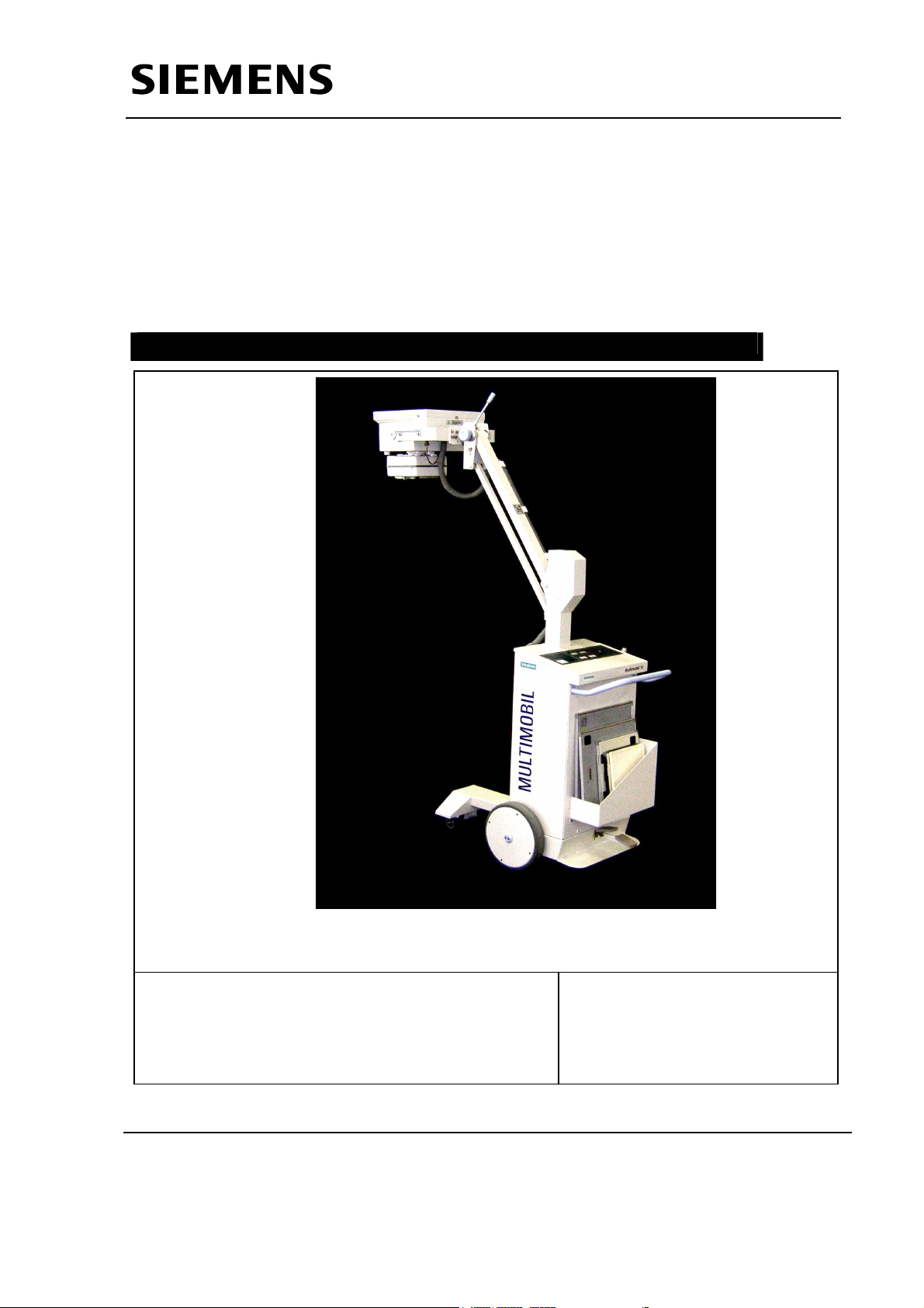
Multimobil 10
Service manual
Circuit Description
Med
Circuit Description
Version :4.0
The reproduction, transmission or use
of this document or its contents is not
permitted without express written
authority. Offenders will be liable for
damages.
Siemens Ltd. Med Division India Version 4.0
Page 1 of 25
Page 3

Service manual
Circuit Description
INDEX
1 MASTER CARD D915............................................................................................................................. 4
1.1 GENERAL DESCRIPTION: ................................................................................................................. 4
1.2 FUNCTION DESCRIPTION:................................................................................................................ 4
1.2.1 POWER SUPPLY: .......................................................................................................................... 4
1.2.2 RESET GENERATION: ................................................................................................................. 5
1.2.3 CRYSTAL OPERATION:............................................................................................................... 5
1.2.4 MICROCONTROLLER: ................................................................................................................ 5
1.2.5 OCTAL LATCH: ............................................................................................................................. 5
1.2.6 GAL: ................................................................................................................................................. 5
1.2.7 EPROM:........................................................................................................................................... 6
1.2.8 NVRAM:........................................................................................................................................... 6
1.2.9 KEYBOARD:................................................................................................................................... 6
1.2.10 DISPLAY(RADIOGRAPHY) :.................................................................................................. 6
1.2.11 SERIAL COMMUNICATION : ................................................................................................ 6
1.2.12 kV SOLL AND mA SOLL:......................................................................................................... 6
1.2.13 kV FEEDBACK :........................................................................................................................ 7
1.2.14 IH FEEDBACK:......................................................................................................................... 7
1.2.15 mA FEEDBACK: ....................................................................................................................... 7
1.2.16 kV REGULATION: .................................................................................................................... 7
1.2.17 FILAMENT REGULATION: .................................................................................................... 8
1.2.18 mAS INTEGRATION :............................................................................................................... 8
1.2.19 CONTROL OF THE FIRING FREQUENCIES REG and CAL:........................................ 8
1.2.20 GENERATION OF ACTUAL FIRING SIGNALS : ............................................................... 8
1.2.21 SHORT CIRCUIT FEEDBACKS (SCM,SCH) : .................................................................... 9
1.2.22 KV, MA MAX FEEDBACK (KVM,JIM ) ..................................................................................... 9
1.2.23 GENERATION OF ROTATING ANODE DRIVING AND CONTROL SIGNALS: .................... 10
1.2.24 ROTATING ANODE CURRENT FEEDBACKS : ...................................................................... 10
1.2.25 Line voltage monitoring ............................................................................................................. 10
1.2.26 Capacitor Bank Voltage Monitoring.......................................................................................... 10
2 MAIN INVERTER PCB D960 .............................................................................................................. 12
2.1 GENERAL DESCRIPTION: ............................................................................................................... 12
2.2 FUNCTION DESCRIPTION:.............................................................................................................. 12
2.2.1 Main Inverter: ................................................................................................................................. 13
3 FILAMENT INVERTER AND ROTATION CARD D801 ................................................................ 14
3.1 GENERAL DESCRIPTION: ............................................................................................................... 14
3.2 FUNCTION DESCRIPTION:.............................................................................................................. 14
3.3 ON -- OFF CIRCUIT: .......................................................................................................................... 14
3.4 DC -- DC CONVERTER...................................................................................................................... 15
3.5 FILAMENT INVERTER CIRCUIT: ................................................................................................... 15
3.5.1 Short circuit Detection and Protection : ........................................................................................ 16
3.5.2 Filament current (Ih) Feedback:..................................................................................................... 16
3.6 ROTATING ANODE CIRCUIT:......................................................................................................... 16
3.6.1 Rotating Anode Current Feedback: ................................................................................................17
3.6.2 CONTROL SIGNALS FOR THE RELAYS: ..................................................................................... 17
3.6.3 VOLTAGE MONITORING SIGNAL:.............................................................................................. 17
4 CHARGER PCB D950A (125 MAS)...................................................................................................18
Siemens Ltd. Med Division India Version 4.0
Page 2 of 25
Page 4

Service manual
4.1 GENERAL DESCRIPTION: ............................................................................................................... 18
4.2 FUNCTION DESCRIPTION:.............................................................................................................. 18
4.2.1 Power circuit:.................................................................................................................................. 18
4.2.2 CONTROL CIRCUIT ...................................................................................................................... 19
4.2.3 FEEDBACK CIRCUIT:................................................................................................................... 19
5 KEYBOARD PCB D936 ........................................................................................................................ 21
5.1 GENERAL DESCRIPTION ................................................................................................................ 21
5.2 FUNCTION DESCRIPTION............................................................................................................... 21
5.2.1 Keypad............................................................................................................................................. 21
5.2.2 Interface with Master Card ............................................................................................................. 21
6 DISPLAY CARD D932 .......................................................................................................................... 22
6.1 GENERAL DESCRIPTION ................................................................................................................ 22
6.2 FUNCTION DESCRIPTION............................................................................................................... 22
7 KV-MA FEEDBACK PCB D800 ......................................................................................................... 23
7.1 GENERAL DESCRIPTION ................................................................................................................ 23
7.2 FUNCTION DESCRIPTION............................................................................................................... 23
7.2.1 KV Feedback at R+, S, R- ............................................................................................................... 23
7.2.2 mA Feedback at P and N............................................................................................................... 23
Circuit Description
8 TERMINAL PCB D900A..................................................................................................................... 24
8.1 GENERAL DESCRIPTION ................................................................................................................ 24
8.2 FUNCTION DESCRIPTION............................................................................................................... 24
8.2.1 U , V ................................................................................................................................................ 24
8.2.2 11, 12............................................................................................................................................... 24
8.2.3 0 , I, II.............................................................................................................................................. 24
9 SWITCH MODE POWER SUPPLY D980 .......................................................................................... 25
9.1 GENERAL DESCRIPTION : .............................................................................................................. 25
9.2 FUNCTION DESCRIPTION :............................................................................................................. 25
Siemens Ltd. Med Division India Version 4.0
Page 3 of 25
Page 5

Service manual
Circuit Description
1 Master Card D915
1.1 GENERAL DESCRIPTION:
The Master Card D915 forms the main closed loop control system in the entire
X ray generator MULTIMOBIL 10.
1.2 FUNCTION DESCRIPTION:
The functions performed by D915 are as follows:
1.The microcontroller 80552 ( J31) on D915 executes the program which makes
the Xray generator work. J31 also genarates and receives proper signals for
most the activities of MULTIMOBIL 10.
2.The EPROM stores the entire bios software.
3.The Nonvolatile RAM stores all the temporary variables while execution of the
main program. Even at power OFF,it stores the last display-data.
4.The peripheral Ics along with J31 are used for generation of the driving signals
for
1. Main Inverter
2. Filament Inverter
3. Rotating Anode.
Additionally the peripheral ICs receive the feedback signals from the output
processes and feed it back to J31 for taking proper corrective action.
5. The faults such as accidental short circuit, mismatching of the actual value and
the reference value of KV,mA,or ms, improper operation of any
process are reported to the Master card for indicating error to the operator and
for taking necessary action ,if feasible.
6. The functions performed by D915 are as follows:
a) Accepting the key pressed by the operator through D936
b) Display the proper Radiography through D932
c) Genarating the reference values of KV (KVS) and mA (JRS) and
converting them to the driving pulses of the Main and the Filament
Inverter.
d) Accepting actual values of the set parameters and regulating the required
parameters.
1.2.1 POWER SUPPLY:
The +15,0V,-15V and +5V,0V voltages are obtained from the SMPS through the
connector X15.
The +Vp supply of 15V is obtained through X10 from the Filament Inverter and
Rotation card D801.
The reference voltage for the Microcontroller (J31) is 5V and it is generated by
R119 , C85, and J30.
Siemens Ltd. Med Division India Version 4.0
Page 4 of 25
Page 6

Service manual
Circuit Description
1.2.2 RESET GENERATION:
The RST signal is generated by IC J40 (MAX 700 :power supply monitor with reset)
at power ON. The switch SW2 also allows for manual reset of the system.
On actuating SW2 ON, reset is generated by J40 which is applied to RST pin of
J31.
1.2.3 CRYSTAL OPERATION:
The 12 Mhz Quartz crystal forms a Pierce Oscillator along with the two capacitors
C93 and C95.The output of the oscillator is a 12Mhz sinusoidal wave which is
applied to XTAL1 and XTAL2 inputs of J31 for providing timings for internal
operations of the microcontroller.
1.2.4 MICROCONTROLLER:
The microcontroller J31 outputs demultiplexed lower order address bus and the
data bus on port ‘ P0’ and higher order address bus on port ‘P2’.
The control signal
RD , WR along with A8-A15 are provided to J28 (GAL) to
generate the chip select signals for accessing various peripherals.
The status signal
PSEN
is used for reading external program stored in EPROM
J32.
EA ‘LOW’ allows accessing the external program memory.
The
Different signals for controlling various operations of the entire system are provided
by the Microcontroller on its ports P1,P3-P5.
The analog inputs AN0-AN6 are used for monitoring analog signals.
The pins TXD and RXD are used for serial communication between the processor
and the external device such as a Computer or any pocket terminal (for servicing).
The Service switch ST provided at pin P4.5 is used for operating the Unit in the
service mode.
1.2.5 OCTAL LATCH:
The multiplexed address and the data bus is separated by the octal latch J27.
At the active ALE signal ,the lower order address (A0-A7) is latched.
1.2.6 GAL:
Since Memory mapping technique is used,the chip select signals for various
peripheral devices are generated by the Gated Array Logic IC J28.The inputs are
the address lines (A8 - A15) ,and the control signals
CS1 to CS8 . These output chip select lines are generated on the basis of the
are
RD and WR . The output lines
logic implemented in the program stored in the GAL.
Siemens Ltd. Med Division India Version 4.0
Page 5 of 25
Page 7

Service manual
Circuit Description
1.2.7 EPROM:
The entire program is stored in a single EPROM J32.
1.2.8 NVRAM:
The Two Kbyte NVRAM stores the variables the operation of the unit.
A0 - A10 and D0 -D7 are the address and the data lines provided to the RAM.The
first 2 Kbytes of entire memory space 0000H to 07FFH is used as RAM.
1.2.9 KEYBOARD:
The keys are accepted through X12 from D936.
The keys ( KV+ , KV -, mAS+, mAS-,DL_SERV ) are accepted on the data bus
through J38 and J37at the address 9000H.
The ON, OFF signals are routed via X12, D915, X10 to D801.
1.2.10 DISPLAY(RADIOGRAPHY) :
The data bus, the control signal WR and the chip select signal CS2 are provided to
the Display Driver J24 on D932 through X1.Writing the control word and the string
of 8 byte data at the addresses 8000H and 8800H respectively displays the KV and
mAS values and lights up function related LEDs on D915.
1.2.11 SERIAL COMMUNICATION :
TXD , RXD are provided to the serial communication port of D915.Various activities
of the unit can be controlled by an external device such as a PC or a pocket
terminal.The serial port is meant for testing and service purposes.
1.2.12 kV SOLL AND mA SOLL:
The KV soll and mA soll values are generated by Dual Digital to Analog Converter
J17 and the Opamp J13 acting as I - V converter.
The microcontroiler J31 outputs the digital values of KV soll and mA soll on the
data bus at address A000H (
CS3) and A100H ( CS4 ) respectively.The reference
current for DAC is adjusted by means of presets P6 and P7.
The KV soll and mA soll are fed back to the AN3 and AN4 pins of J31 for ensuring
their proper values.These soll values are also used for regulation of KV and mA.
The KV soll ratio is 1 V = 30 KV and
The mA soll ratio is 1 V = 50 mA
Siemens Ltd. Med Division India Version 4.0
Page 6 of 25
Page 8

Service manual
Circuit Description
1.2.13 kV FEEDBACK :
The actual KVp across the tube is stepped down and fed back in the form of KV/2+
and KV/2- to the Master card D915 at pins 1and 2 as PKV and NKV respectively
with respect to the common terminal at pin 3.
PKV and NKV are passed through the voltage follower J5 and then fed to the
Differenial Amplifier formed by J5 to produce Kvist,which is used for KV regulation
(KVist ratio is 1V= 20 KV)
KV ist is fed back to AN7of J31 for monitoring purpose.
1.2.14 IH FEEDBACK:
The Filament current (Ih) feedback is taken from the Filament inverter and rotation
PCB through X11.1.J7 provides a gain of 5 to Ih.
The AC Filament current Iheiz is converted into DC value Ih by RMS - DC converter
J6.J9 provides an approprate gain to Ih (that can be adjusted by preset P5)
so that the ratio 1V = 2A holds true. Ih is fed back to J31 at AN2 for monitoring
purpose,the same is used for Ih regulation.
1.2.15 mA FEEDBACK:
The tube current (JR) is fed back in the form of voltages P+ and N- at pins 5 and 6
of X8 on D915. P+ and N- are applied to the Differential Amplifer formed by J4.
The output JR represents the actual tube current mAist which is fed back to J31 at
AN1 through J9 for monitoring purpose.JR is also used for tube current regulation.
1.2.16 kV REGULATION:
The KV soll and KV ist values are fed to the P-I controller formed by IC J10.
The difference between the KVist and KV soll value is amplified to produce an
appropriate error output , so as to compensate the error. The zener V12 limits the
maximum ouput voltage of the error amplifier to 10V.
The error amplifier output is fed to PLL IC J3 which is used as voltage to frequency
converter.
The J10 output voltage produces an equivalent frequency REG at J3 output.
For 10V, REG(the maximum firing frequency of the Main Inverter) is 15khz.
J3 is enabled by an active low INH2 signal provided by the microcontroller J31 at
P4.1 through J23.During HT, J3 is enabled through INH2 and J3 results in a firing
frequency of Main Inverter IGBTs, to result in actual KV in line with the required
value.
Siemens Ltd. Med Division India Version 4.0
Page 7 of 25
Page 9

Service manual
Circuit Description
1.2.17 FILAMENT REGULATION:
Filament Regulation is divided into two parts:
1. Regulation without high voltage : The filament current Ih is regulated.The CPU
J31 outputs required filament current value on input of DAC.
2. The actual tube current JR is regulated.J31 outputs the required tube current on
the input of DAC.Depending upon whether the regulation is pre H.T or post H.T
either Ih or JR is selected through Heiz signal from J31 (P4.4) and used for
regulaton together with the corresponding value from the DAC.The output of the
error amplifier J10 is fed to PLL J2 which is configured as voltage to frequency
converter.The PLL J2 is enabled through INH1 signal from J31(P4.0) and
generates a frequency in line with the output of error amplifierJ10 to result in
required filament current or the tube current.
1.2.18 mAS INTEGRATION :
The actual tube current is applied to the input of V-F converter J1. The transfer
ratio ( Frequency to Voltage) of J1 is adjusted by preset P1.The output frequency is
selected by J8 only when the KVist reaches 75% of its final value.
The output of J8 is fed to J31 as timer 0 clock .The timer 0 inside J31 is configured
as timer counter which is preloaded with a count equivalent to mAs value.The
incoming clock decrements the counter and on reaching ‘0’,generates an interrupt
to terminate the exposure.
1.2.19 CONTROL OF THE FIRING FREQUENCIES REG and CAL:
REG is controlled by the signals INH2 and INH3 and it is enabled only when
INH2=0 and INH3 =1 .CAL is enabled only when INH1=0.
1.2.20 GENERATION OF ACTUAL FIRING SIGNALS :
1.2.20.1
Main Inverter Firing Frequency :
The pulse duration of the actual firing signals of the Main Inverter is decided by the
Monoshot Multivibrator J21 (IC 4538 Dual Monoshot Multivibrator) and R104,C66
and R105,C67.
RST pin of J21 is normally high for its proper operation.
The
The outputs of J21 at pins 6 and 10 are out of phase. These signals are optically
isolated by J39 and J41 and fed to the Main Inverter Driver (D960) through X20.14
and X20.18.
The supply for the isolated ouput of J39 and J41 is obtained from the Filament
inverter and Rotation card D801.
Siemens Ltd. Med Division India Version 4.0
Page 8 of 25
Page 10

Service manual
Circuit Description
1.2.20.2 Filament Inverter Firing Frequency:
J18 is used to determine the pulse width of the the actual firing signals of the
Filament Inverter.The IC J20 ensures that the firing pulses of the Filament Inverter
are out of phase.These signals are inverted by J22 and fed to the Filament Inverter
firing circuit on D915 through X11.13 and X11.16.
1.2.21 SHORT CIRCUIT FEEDBACKS (SCM,SCH) :
1.2.21.1 SCM :(Main Inverter Short Circuit)
During normal operation,the transistor V38 is ON and simultaneously the
optocoupler is also ON.
An active LOW error signal at X20.16 turns V39 and consequently J34 OFF.The
J34 output becomes LOW to give the HIGH SCM (Main Inverter short circuit) signal.
SCM is inverted by J22 and then it is fed back to the microcontroller J31(at P3.3) for
taking the corrective action.
The three signals SCM , KVM and JIM are used for disabling the Driving pulses of
the Main Inverter. This is done by OR ing of these three signals by J14. At the
occurrence of either of these three signals ,
RST of J21 goes LOW and its output is
disabled.
1.2.21.2 SCH (Filament Inverter Short Circuit):
During the short circuit of either of the two IGBTs forming the Filament Inverter on
D801,the short circuit signal generated by the two drivers on the Filament inverter
and Rotation Card D801 are fed back to the Master card through X11.12 and
X11.14 .
SCH is obtained on ORing of these signals by J14. SCH gives an interrupt at (P1.1)
to J31 .
SCH also resets J18, thus disabling the Filament Inverter driving pulses.
1.2.22 KV, MA MAX FEEDBACK (KVM,JIM )
1.2.22.1 KVM (Maximum KV):
If the KVN and KVP values exceed the reference value of 4.54V(68.5kV) at J12
(Comparator) its output generates the KVM signal. KVM is also fed back to J31 at
P32 as T0 Interrupt for initiating necessary corrective action like stopping the
exposure instantaneously.
Siemens Ltd. Med Division India Version 4.0
Page 9 of 25
Page 11

Service manual
Circuit Description
1.2.22.2 JIM (Maximum mA):
An increase in IH or JR more than the reference values respectively generates JIM.
JIM is fed as T3 interrupt to J31.
1.2.23 GENERATION OF ROTATING ANODE DRIVING AND CONTROL
SIGNALS:
J31 generates ARR/ (Accelarate Anode signal ) at P4.6 and FR/ (Brake Anode)
at P4.7 respectively.These signals are driven by the driver J23. and are applied to
the optotriacs on D801 through X11.8 , X11.10 and X11.7 respectively.The signal at
X11.8 is delayed by R128 and C99 combination to fire the second triac after the first
on D801
1.2.24 ROTATING ANODE CURRENT FEEDBACKS :
From D801, the rotating anode alternating current is fed back in the form of AC
voltage.These feedback voltages are available at X11.5 and X11.3 respectively and
they are applied to J11. J11 limits the negative half of the input signal to 0.7 V while
it provides the gain of 4 to the positive half cycle of the input signal.
The I1and I2 signals are as shown in the enclosed sheet.
I1 and I2 are compared with the reference values and then converted into
equivalent DC voltages by V16,R73,C46 and V14,R67,C40 combinations.RT1 and
RT2 are the feedback voltages applied to J31 at P1.6 and P1.5 respectively to
ensure proper anode rotation.
1.2.25 Line voltage monitoring
The actual mains Line voltage stepped down & converted to DC and through
differential amplifier is passed through the voltage follower J29 and then fed to
the AN5 pin of J31 for display the line voltage (for both 110 and 230 V) during first
step of hand release switch for radiography. If the measured Line voltage is less
than 205 volts on 230 V line, microcontroller sends a signal at P5.1 to switch ON the
LN contactor which will support extra voltage through auto transformer for 10 KW
power generation. In preperation and exposure mode contactor retains its position.
After 5 second of each termination of radiography Line voltage is monitored once
again.
LN contactor does not pick up when the unit is connected to 110 V supply.
1.2.26 Capacitor Bank Voltage Monitoring
The actual voltage stored in the capacitor bank is stepped down & converted to
measurable DC and through differential amplifier it is passed through the voltage
follower J29 and fed to AN6 pin of J31 a signal Vc. If capacitor Voltage does not
Siemens Ltd. Med Division India Version 4.0
Page 10 of 25
Page 12

Service manual
Circuit Description
build up within 3.5sec or if the measured voltage more than 350V DC then a Error
Code is generated and further charging of Capacitor Bank is terminated by disabling
CAR signal at P4.4 of J31
KV soll : 1V = 30 KV
2V
mA istl: 1v=50 mA
3.2V
100 ms
KVp:
3V
KVN: 3V
Kvist:
3V
TYPICAL WAVEFORMS :for
60 KV 16 mAS 160mA 100ms
Siemens Ltd. Med Division India Version 4.0
Page 11 of 25
Page 13

Service manual
Circuit Description
2 Main Inverter PCB D960
2.1 GENERAL DESCRIPTION:
The Main Inverter Driver D960 is used for driving the IGBT based Full Bridge
Inverter.The driving pulses for the Main Inverter and the supply voltage +Vp are
obtained from the Master card (D915) through X20.
The DC voltage at the output of the capacitor bank D970A is converted into High
frequency AC voltage by means of the Main Inverter.
2.2 FUNCTION DESCRIPTION:
DISP1 and DISP2 are the Main Inverter driving pulses obtained from the Master card
through X20.14 and X20.18.These pulses are out of phase.
DISP1
+15V
40 uSec
DISP2
40
uSec
Siemens Ltd. Med Division India Version 4.0
Page 12 of 25
Page 14

Service manual
Circuit Description
The IGBT drivers SKHI 22 A ( Z01 and Z02) are used for:
1.Driving the pairs of IGBTs .The Gate signals of IGBTs DISP1 and DISP2 are
boosted by these drivers.
2.Detecting any short circuit of the IGBTs by means of sensing the voltage
between Collector and Emitter.If Vc-e = 0, the ERR/ pin of SKHI 21 goes LOW.
This active low signal is reported to the Master Card through X20.16 for
disabling the firing pulses of the Main Inverter.
3.Providing isolation between the input low voltage digital circuit and the output
high voltage power circuit.
2.2.1 Main Inverter:
The main Inverter uses IGBT module SKM75GB 123D as the switching device.
Each module has two IGBTs and two diodes in antiparallel.Two IGBTs connected
in parallel form one arm of the Full Bridge Inverter.The IGBTs top V3 ,V4 and
bottom V1,V2 are fired by DISP1 whereas bottom V3,V4 and top V1,V2 are fired by
DISP2.
The DC supply for the Bridge Inverter is obtained from the output of D970A
(Capacitor Bank).The primary of the HT Transformer forms the Load of the Main
Inverter along with the resonance capacitor C5 and Inductor L1
U ,V current waveform:
75µ Sec
top bottom
V3,V4; V3,V4;
bottom top
V2,V1 V2,V1
Siemens Ltd. Med Division India Version 4.0
Page 13 of 25
Page 15

Service manual
Circuit Description
3 Filament inverter and Rotation Card D801
3.1 GENERAL DESCRIPTION:
The Filament inverter and Rotation Card D801 contain electronic circuits for
controlling
Filament Inverter,
Rotating Anode,
NS and CS contactors. D801 also contains the power distribution part of the entire
system.
3.2 FUNCTION DESCRIPTION:
The voltages provided by D801 to other PCBs are as follows:
1 220 V AC for SMPS (D980).
2 +15 V (Vp) for Main Inverter driver (D960).
The input supply to D801 is obtained from the secondary windings of the Main
transformer T2.
When the MCB is switched
ON, the 24V AC supply gets applied from the output of the
Mains transformer through a powermat connector to D801 through connector X1.5 and
X1.6. This 24V AC voltage is rectified by
capacitor
C21. The DC voltage across C21 is 33V.
V49 (full wave rectifier) and then filtered by
J16 (IC LM 317 voltage regulator) is used to provide exact DC voltage of 24V from
33V input .The presence of DC voltage at the output of the regulator J16 is indicated
by LED
V50
3.3 ON -- OFF CIRCUIT:
The mains ON/ OFF signals I and 0 are available at X10.4 and X10.2. These signals
control the relays
K5 (ON) and K1 (OFF). An additional relay K4 switched ON by K5
turns the NS contactor ON.
The supply voltage built around J14 (LM317) is used as an input for the DC - DC
Converter and also as
Vp voltage for the Main Inverter Driver D960.
The mains voltage of 220 V ac appears across X50.1 and X50.3. When Unit ON
switch is pressed, the circuit for Relay Coil K5 gets completed as the coil K5
energises the contact K5 (6,8) is establised and hence the unit remains ON even if
the switch is released and causes the Relay K4 to energise. This causes the
contactor NS to close and provide the ac voltage to the Filament Inverter and other
circuit points like SMPS input and Contactor Coil connections.
Siemens Ltd. Med Division India Version 4.0
Page 14 of 25
Page 16

Service manual
Circuit Description
When the OFF switch is pressed, the Relay K1 coil is energised and this causes the
Normally Closed contact K1 (6,8) of relay K1 to open thereby opening the circuit
connections for relay K5. The Unit thus is turned Off.
3.4 DC -- DC CONVERTER
The +15 V supply is switched by MOSFET V7 which drives transformer T3(1:1:1) at
a frequency of about 75 KHz. The oscillator frequency and drive for the Mosfet is
provided by J10 (IC 4584).
The two isolated +15V supply voltages (+VS1 and VS2) generated are used for the
driver circuit of upper and lower arm of the half bridge filament inverter.
The fuse F6(800mA) protects against any short circuit in the DC- DC converter.
3.5 FILAMENT INVERTER CIRCUIT:
The 220V AC supply obtained from X1.2 and X1.3 or X1.4(when input supply <205V)
is rectified using bridge rectifier V29. The fuse F1 of 6A prevents the overcurrent.
The LED V31 indicates the presence of 220V at the input.
The IGBTs V11 and V19 along with capacitors C14, C12 and C13, C15 form the Half
Bridge Inverter circuit.The varistors U7 and U6 are used to suppress the overvoltage
spikes.The thermistors R31 and R32 limit the in rush current in the capacitors.
LEDs V23 and V24 in series with R29 and R30 respectively indicates the presence of
the DC supply of about 330 V to the filament inverter.
The gate pulses for the two IGBTs are obtained from the Master card (D915)
through X11(pins 13 and 16).
These gate pulses are out of phase.
The optocouplers provide isolation between the power circuit and the digital circuit.
The +15V supply to the input of optocouplers J9,J7,J12,J13(HCPL 2211) is obtained
through X11.15
The IGBT gate drivers J8 and J11 ( both IR2121) are used for driving V11 and V19
and also for sensing any short circuit .
The isolated supply of +15V for the drivers(J8,J11) is obtained from DC-DC converter.
The frequency of the gate driving signals is determined by
CAL in the Master card.
V20 and V12 are over voltage protection zener diodes for gates of IGBTs. V8 and
V18 are the free wheeling diodes. The current flows through these diodes when
IGBTs across them are OFF.
V14 and V22 avoid excessive voltage (above 440V) appearing across each IGBT
when the other IGBT turns OFF. The filament inverter output current flows through
the primary winding of the filament transformer through X5.1 and X5.2
Siemens Ltd. Med Division India Version 4.0
Page 15 of 25
Page 17

Service manual
Circuit Description
3.5.1 Short circuit Detection and Protection :
IGBT Drivers IR2121 senses any short circuit in the filament inverter. The current
sensing resistors R17 and R23 are connected in the path of the filament current.
The drop across these resistors is sensed for detecting any short circuit. If voltage
at pin CS(current sense) of IR2121 increases above 0.23V then ERR signal is
generated by it and the driving pulses at the output are disabled.
An 8.2V zener diode is connected at pin 3(ERR) of IR2121 to detect the error signal in
case of short circuit, the capacitors C3,C10 connected at the ERR pins of J8 and J11
respectively charge to a voltage greater than 8.2V. The error signal is isolated by ICs
J7 and J13 and then sent to the Master card through X11.14(for short circuit of V11)
and X11.12(for short circuit of V19).
3.5.2 Filament current (Ih) Feedback:
The Transformer T4(turns ratio 100:1) is used for sensing the primary filament current.
The drop across R13 is sensed and fed to the master card through X11.1 and X11.2
for current (Ih) regulation.
3.6 ROTATING ANODE CIRCUIT:
The 240V AC supply for the rotating anode circuit is obtained at ‘A’ the relay K2 turns
ON. The fuse F3 of rating 2.5A prevents the overcurrent. The LED V32 gives the
indication of the input supply.
The rotating anode circuit consists of triacs V1 and V5 which act as a switching
devices. The drive to these triacs are obtained from the optotriacs J1 and J3 and these
are controlled by the signals from the Master card. +15V supply is provided through
X11.9 to the optotriacs.
The acceleration signal ARR (logic LOW) at X11.10 and X11.8 causes J1 and J3 to
cunduct which in turns provides the gate firing pulses to the main Triacs V1 and V5.
The signal applied at X11.8 is delayed in the Master card. The conduction of
theseTriacs result in AC voltage of 240V appearing at X3.1 and X3.2 with respect
X3.3. X3.3 is connected to 0V through relay K2. X3.1 is connected to the main
winding through a 10µF capacitor and X3.2 is connected to the auxillary winding of
stator.
The application of 220V AC supply at X3.1 and X3.2 w.r.t. X3.3 starts anode rotation.
The current
I1 flows through main ` winding and current I2 flows through auxillary
winding of the stator. The braking signal (FR:logic LOW) turns J5 ON which fires the
Triac V5 in one half cycle due to diode V4 . The DC voltage at the output of Triac V5
is used for braking the rotating anode. The metal oxide varistors U1 and U2 protect the
Triacs from high voltage surges.
Siemens Ltd. Med Division India Version 4.0
Page 16 of 25
Page 18

Service manual
Circuit Description
3.6.1 Rotating Anode Current Feedback:
The current transformers T1 and T2(turns ratio 250:1) are used for taking the
feedback of stator winding
I1 and I2. The drop across resistors R1 and R2 connected
at the secondary of current transformers is sensed and fed to the Master card through
X11.3 , X11.4 (
I1) and X11.5 ,X11.6 (I2) for detecting the errors.
3.6.2 CONTROL SIGNALS FOR THE RELAYS:
+24V DC supply is provided to the control coils of the relays K3, K2 and CS1 through
the optocouplers J4, J6 and J2.The optocouplers driven by the signals from the Master
card. The relay K3,K2 controls the supply 240V AC to the LN contactor and Rotating
anode circuit respectively and CS1 is used for making the contactor CS ON in
Multimobil 10
3.6.3 VOLTAGE MONITORING SIGNAL:
Unregulated DC Power Supply 33V dc from the out put of V49 is used and attenuated
to 3.7V (approx) at 240V input AC. Attenuation is achieved by resistor network (R51
and P1 on D801) and Op-amp J17.Output of this Op-amp is fed to D915 through
X10.17 and this signal V_BAT is fed to microcontroller on Analog Port 5 and this signal
is polled for every 5 sec and updates the display for mains voltage.
Siemens Ltd. Med Division India Version 4.0
Page 17 of 25
Page 19

Service manual
Circuit Description
4 Charger PCB D950A (125 mAs).
4.1 GENERAL DESCRIPTION:
The Charger card D950A contain following electronic circuits for Charging entire
Capacitor Bank,
Power Circuit
Control Circuit
4.2 FUNCTION DESCRIPTION:
4.2.1 Power circuit:
1. Single Phase 220V AC supply is obtained through X3.2 and X3.6 from the
mains through CS Contactor.
2. The maximum input current is 10A, as specified by Fuse F1.
3. C39, L2, C38 form a PI section filter for suppressing the transient, if any.
4. The NTC thermistors R49 and R41 initially limit the input current passing
through the bridge rectifier V20. The capacitor C32 charges to the maximum
peak value of approx. 310V. This is indicated by LED V24.
5. This 310V DC voltage is applied to a series circuit of an Inductor L1 and and the
IGBT V3. The HALL TRANSFORMER J10 is used for sensing the current
through the inductor L1, the current ratio being 500:1 (primary/secondary).
6. The gate pulses of the IGBT are provided by a separate control circuit.
7. R19, R20, C20, C21in series form a snubber circuit, and it is connected across
the switching device (V3) for protection purposes.
A back to back diode V15 connected across L1 restrict the building of excessive
voltage across inductor L1.
8. The switching device (IGBT V3) is operated at a fast rate of 25Khz with 75%
duty cycle,by the control circuit.
When V3 is ON , current of approx. 10A passes through the inductor L1. During
L
I
thgis time L1 stores the energy (=1/2
*
9. During the off period of V3, the stored energy in L1 is used to charge the
Capacitor Bank on D970A. The capacitor bank is connected across B1 – B2.
10.The capacitor bank charges to a maximum Voltage of 355V, and the charging
current upto 16A.
11. Diode V5 prevents the reverse discharging of the capacitors.
Capacitor voltage indication is given by LED V25.
12. A resistor of 470 Ohms /200 W is connected across B2 and B1,through NS
contactor for discharging the voltage across the capacitor bank during turn off.
X3.1 and X3.4 are shorted through a NC contacts(opened during the normal
operation of the unit) for discharging.
I)
*
*
Siemens Ltd. Med Division India Version 4.0
Page 18 of 25
Page 20

Service manual
Circuit Description
13.The 400V Over voltage protection diode V9 is connected to prevent the
excessive charging.
4.2.2 CONTROL CIRCUIT
4.2.2.1 DRIVING CIRCUIT:
1. The charging process of the capacitor bank is controlled by the control circuit
in accordance with control signals from the MASTER CARD D915.
2. The charging process ON signal from the master card (CAR=1),gates the
basic signal FR1 of 25 Khz and 25% duty cycle. FR1 is obtained by the circuit
comprising of IC J13( 2 input NAND gate),and C35,and R38,V17 , R40 , V16.
3. FR1 is applied as one of the inputs to IC J16(triple input OR gate),the other
inputs being an “OK” signal (if the capacitor bank is fully charged),and the
“ERR”(error) signal (in case of any error).If any of the avove three signals is
continuously high (=1),the charging operation is stopped.
4. During normal charging operation ERR=0, OK =0.
FR1 is applied to the reset input of a D-F/F (IC J15).
FR1 is also applied to a delay circuit (lag network) consisting of R39 and
C34. The delayed signal on inversion (by IC J12) is applied as a clock (CLK)
input of J15(D/FF).
5. The output of D-F/F is inverted (by IC J13) and then applied to an optocoupler
J6.
6. The isolated output is a rectangular wave of 30
µs ON time and 10µs OFF time.
7. This signal on boosting by a driver (IC J2), drives IGBT V3 ,
4.2.3
FEEDBACK CIRCUIT:
A) “ OK ” (CAPACITOR BANK FULLY CHARGED):
(
Vc = 3.3V,OK=1)
The Voltage across the Capacitor Bank is fed to a differential amplifier(J4) with
optical isolation. The outputs of J4 is further processed by another differential
amplifier(J8). The output of J8 is fed to a comparator J11 as inverting input and
whose non-inverting input is held at a fixed reference voltage. Once the capacitor
bank voltage is higher than a fixed value the active “high” is generated at output of
J12.2 as “OK” signal.
B) ERRORS(ERR=1)
1. OVER VOLTAGE :
The voltage across capacitor bank is also fed to an optocoupler J3 through two
Zener diodes V1 and V2. When the voltage exceed far more than the sum of the
Zener voltages , the optocoupler J3 conducts and an active “High” signal is
generated at the output of J12.12 which is fed as one of the input of the OR gate
J16.
Siemens Ltd. Med Division India Version 4.0
Page 19 of 25
Page 21

Service manual
Circuit Description
2. TEMPERATURE :
The Power components IGBT V3 and Diode V5 are mounted on a heat sink whose
temperature is monitored through a NTC Resistor R12. Through a comparator J11,
the reference voltage is compared with the the voltage generator through the
potential divider comprising of resistance R30 and NTC R12. The output of the J11
is fed as another input of OR gate J16.
3. SHORT CIRCUIT OF THE SWITCHING DEVICE :
Excessive flow of current through IGBT V3 is detected through its emitter voltage. The
Driver IR2121 senses any short circuit in the IGBT V3. The current sensing resistors
R11 and R56 are connected in the path of the IGBT V3. The drop across these
resistors is sensed for detecting any short circuit. If voltage at pin CS(current sense) of
IR2121 increases above 0.23V then ERR signal is generated by it and the driving
pulses at the output are disabled.
The driver J2 generates an active high output at pin 3 in case there is a short circuit
in IGBT (V3). This drives the opto-coupler J5 and result in an error signal and is
connected to the input of OR gate J16.
C) MAINS CURRENT FEEDBACK
The rms current drawn from Mains is controlled through the conduction of IGBT V3.
The current is monitored through a Hall Sensor J10 and the load resistance R37.
The voltage equivalent of the dc current flowing through V3 is compared with a
reference value by a comparator J14. When the current flowing through the IGBT
exceeds the limit, the firing pulses for IGBT are disabled by blocking the oscillator
output FR1.
Siemens Ltd. Med Division India Version 4.0
Page 20 of 25
Page 22

Service manual
Circuit Description
5 KeyBoard PCB D936
5.1 GENERAL DESCRIPTION
D936 houses various keys.These keys are Tactile type keys and are available on
the front panel for the operator.
5.2 FUNCTION DESCRIPTION
5.2.1 Keypad
No. Identification Description Hex Code
1
2
Unit OFF n.a.
Unit On n.a.
3 kV + kV increment F7
4 kV - kV decrement EF
5 mAs + mAs increment FD
6 mAs - mAs decrement FB
7 DL_Serv Service mode select FE
The keys KV+ , KV- , mAs+ , mAs- ,
and are accessible from the top
panel of the unit. whereas the key DL_SERV can be accessed after opening the
top panel.
The input supply to this PCB is +15V and it is obtained through X12.2 from the
Master card D915.
5.2.2 Interface with Master Card
The keyboard switches are connected to the Master Card D915 through X12
connector. The switch action is conveyed to the Master Card by a switching 15
Volts signal. In normal condition when no key is pressed all the key lines are
maintained at LOW. This in turn is reflected at the port 9000H as all high as FFH.
Whenever a key is depressed, it is connected to the 15 V dc line and the
corresponding line on the port 9000H goes low. Thus the cooresponding data code
appears on the Data bus of the Microcontroller which is then read by the controller
through the READ$KEYB routine.
Siemens Ltd. Med Division India Version 4.0
Page 21 of 25
Page 23

Service manual
Circuit Description
6 Display Card D932
6.1 GENERAL DESCRIPTION
D932 consists of KV and mAs seven segment displays (V19,V20,V21 for KV)
and (
The data segments are configured as…
1. mAs Unit
2. mAs tens
3. mAs Hundreds
4. kV Unit
5. kV Tens
V24,V25,V26 for mAS).
6. kV Hundreds
The same data locations are used for error code display also. In such case, the
Error code is displayed.
6.2 FUNCTION DESCRIPTION
IC J24 is used to drive these seven segment displays.The supply voltages,data
inputs ( D0-D7) and the chip select signal CS2/ are obtained at X1 from D915.
The seven segment display data (a,b,c,d,e,f,g)and the display select signals DG1DG7 are generated by J24.
A two pin header is used for making the connections of the exposure LED V34 to
the display card. The LEDs V22,V23,V24,V25 on the Master card are also driven by
J24.
Display Driver IC 7218B and the seven segment displays. The Display driver is
mapped at address 8000H. Thus it is configured to receive the Code at 8000H and
the data values from 8800H.
Siemens Ltd. Med Division India Version 4.0
Page 22 of 25
Page 24

Service manual
Circuit Description
7 Kv-ma Feedback PCB D800
7.1 GENERAL DESCRIPTION
The Terminal Feedback PCB D800 is mounted directly on the single Tank and it
is used for taking the KV and mA feedbacks.
7.2 FUNCTION DESCRIPTION
The D800 PCB is divided into two main Functions : KV feedback and mA feedback
7.2.1 KV Feedback at R+, S, R-
The KV applied to the X RAY tube is actually in the form of
with respect to a common terminal S.
The +KV/2 is divided by means of a resistor divider network formed by
20K resistors.The drop across 20K resistor R1 is taken as the +KV/2 feedback at
terminals R+ (X1.5) and S (X1.3).
The spark gap U1 is used to prevent the excessive feedback voltage.If the voltage
across U1 exceeds 90V, it blows off.
The -KV/2 is also divided by means of a resistor divided network formed by
200M and 20K resistors.The drop across 20K resistor R2 is taken as the -KV/2
feedback at terminals R- (X1.4) and S (X1.6).
The spark gap U2 prevents the excessive feedback voltage.
+KV/2 and – KV/2.
200M and
7.2.2 mA Feedback at P and N
The tube current
During RADIOGRAPHY, this current is made to pass through R3 and R4 (
Jr (mA) completes its path through terminals P and N on D800.
10Ω
each) .
The mA link should be inserted at mA- and mA+ terminals.
The zener V3 is used for protection purpose.
The spark gaps U3 and U4 are used for preventing the excessive feedback.
The zeners V1 and V2 are used for limiting the voltages to 15V.
The mA feedback is taken from P (X1.2) and N (X1.1)
Siemens Ltd. Med Division India Version 4.0
Page 23 of 25
Page 25

Service manual
Circuit Description
8 Terminal PCB D900A
8.1 GENERAL DESCRIPTION
This PCB is directly mounted on the Single tank and it consists of terminals U&V ,
11& I2, 0 I II.
8.2 FUNCTION DESCRIPTION
8.2.1 U , V
The output of the main inverter is applied at U and V terminals.These signals are
then transferred to the respective U and V terminals of the Main HT transformer.
The AC input voltage at U , V is stepped up by the HT transformer,rectified and
then applied to the X RAY tube as the
KV.
8.2.2 11, 12
The output of the filament inverter is applied to the 11 and 12 terminals of this PCB.
These signals are connected to the input of the Filament Transformer.
The AC input current at 11,12 is stepped down by the filament trafo and then
applied to the filament of X RAY tube.This is the filament current
Ih.
8.2.3 0 , I, II
A Single phase induction motor is used for rotating the anode of the X RAY
tube.The control supply for this motor is applied at terminal I through capacitor C7.
The capacitor is used for shifting the phase of the main supply. The main winding
voltage is applied at terminal II directly. The terminal 0 forms the common terminal
for the above two voltages.
Siemens Ltd. Med Division India Version 4.0
Page 24 of 25
Page 26

Service manual
Circuit Description
9 Switch Mode Power Supply D980
9.1 GENERAL DESCRIPTION :
The Switch mode power supply is used to supply + 5 Volts to the controller and
associated circuitry and
9.2 FUNCTION DESCRIPTION :
The following are the specifications of the supplies.
+ 5 V at 3 Amps with Tolerance of 3%
+ 15 V at 0.3 Amps with Tolerance of 10 %
- 15 V at 0.2 Amps with Tolerance of 5 %
± 15 V to the driver circuits.
This output is maintained for the following range of the input conditions.
180 V ac to 260 V ac at 50 Hz
± 5 Hz and an input current of 0.7 Amp rms.
All outputs are protected for short circuit conditions and a sharp repeatitive sound is
heard from the SMPS in the event of short circuit. The circuit behaves normally
upon the removal of the short circuit.
Siemens Ltd. Med Division India Version 4.0
Page 25 of 25
 Loading...