

Page 1
s Com
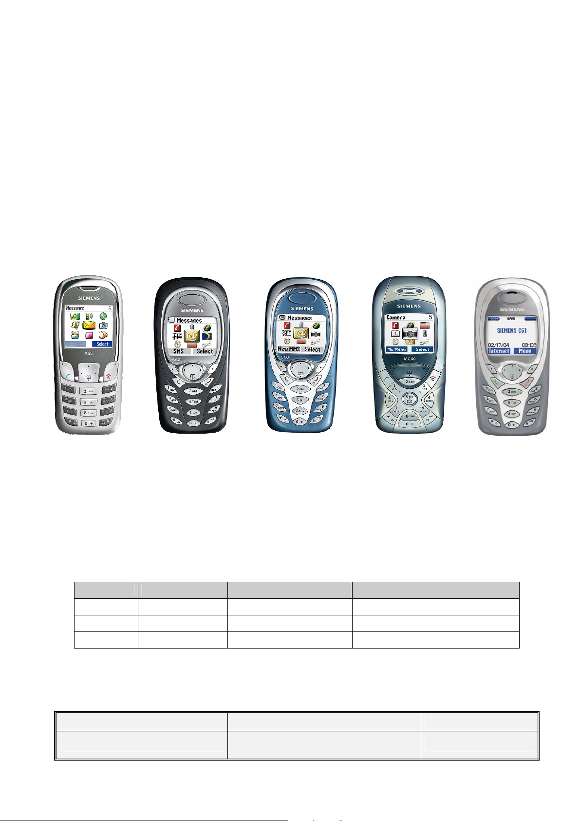
A60/A62/A65/C60/C61/MC60
Level 2.5e
Repair Documentation
V 2.10
Version Date Department Notes to change
V 1.00 08.09.2003 ICM MP CCQ GRM New document
V 2.00 20.01.2004 ICM MP CCQ GRM C61 added
V 2.10 15.12.2004 Com MD CC GRM T Document modified
V 2.1 Page 1 of 61 Com MD CC GRM T
A60/A62/A65/C60/C61/MC60
Company Confidential
Copyright 2004© Siemens AG
12/04
Page 2

s Com
Table of Contents:
1 List of available level 2,5e parts A60/C60 4
2 List of available level 2,5e parts A62/A65 6
3 List of available level 2,5e parts MC60 8
4 List of available level 2,5e parts C61 11
5 Required Equipment for Level 2,5e 13
6 Required Software for Level 2,5e 13
7 Radio Part 14
7.1 BLOCK DIAGRAM RF PART 15
7.2 POWER SUPPLY RF-PART 16
7.3 FREQUENCY GENERATION 16
7.3.1 Synthesizer: The discrete VCXO (26MHz) 16
7.3.2 Synthesizer: LO1 18
7.3.3 Synthesizer: LO2 19
7.3.4 Synthesizer: PLL 20
7.4 ANTENNA SWITCH (ELECTRICAL/MECHANICAL ONLY C61/MC60) 20
7.5 RECEIVER 23
7.6 TRANSMITTER 24
7.6.1 Transmitter: Modulator and Up-conversion Loop 24
7.7 BRIGHT IC OVERVIEW 26
7.7.1 Transmitter: Power Amplifier 27
8 Logic / Control 28
8.1 OVERVIEW OF HARDWARE STRUCTURE 28
8.1.1 Logic Block Diagram A60C60 and C61 28
8.1.2 Logic Block Diagram MC60 29
8.2 EGOLD+ 30
8.2.1 SRAM 34
8.2.2 FLASH 34
8.2.3 SIM 34
8.2.4 Vibration Motor 34
9 Power Supply 34
9.1 POWER SUPPLY ASIC 34
9.1.1 Power Supply Operating modes: 36
9.1.2 Power Supply Functions: 38
V 2.1 Page 2 of 61 Com MD CC GRM T
A60/A62/A65/C60/C61/MC60
Company Confidential
Copyright 2004© Siemens AG
12/04
Page 3

s Com
BATTERY 44
9.2
9.3 CHARGING CONCEPT 45
10 Camera (only MC60) 49
10.1 CAMERA POWER SUPPLY 49
10.2 CAMERA INTERFACES 49
10.3 CAMERA MODULE CONNECTOR 51
11 Interfaces 52
11.1 VIBRA 52
11.2 EARPIECE 52
11.3 MICROPHONE 53
11.4 BATTERY 53
11.5 IO CONNECTOR WITH ESD PROTECTION 54
11.5.1 IO Connector – New Slim Lumberg 54
11.5.2 ESD Protection with EMI filter 55
11.6 SIM 56
11.7 DISPLAY 56
12 Acoustic 57
12.1 MICROPHONE 57
12.1.1 Mechanical 57
12.1.2 Electrical 57
12.2 EARPIECE/LOUDSPEAKER 58
12.2.1 Mechanical 58
12.2.2 Electrical 58
13 Display and Illumination 59
13.1 DISPLAY 59
13.2 ILLUMINATION 60
14 Keyboard 61
V 2.1 Page 3 of 61 Com MD CC GRM T
A60/A62/A65/C60/C61/MC60
Company Confidential
Copyright 2004© Siemens AG
12/04
Page 4
s Com
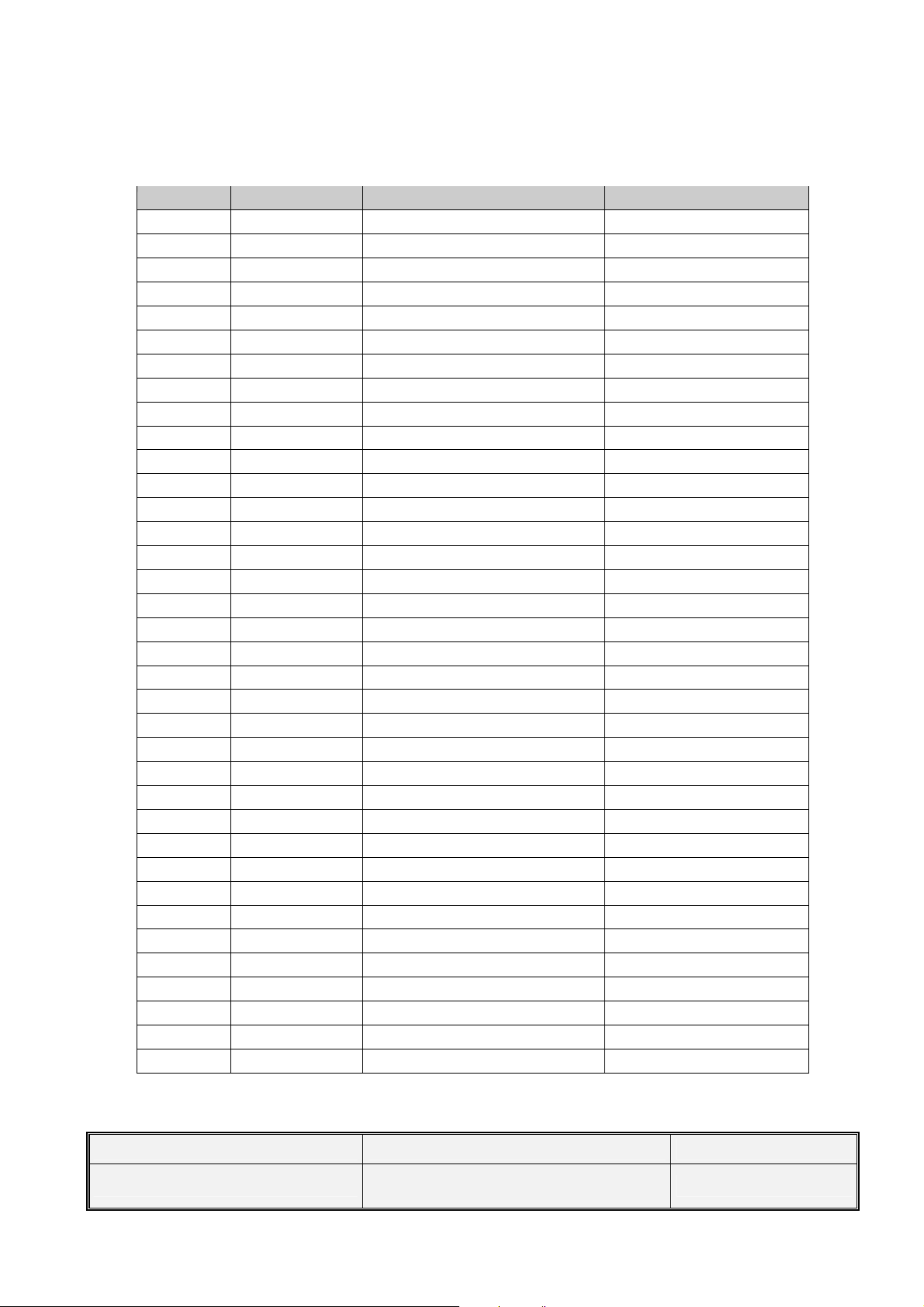
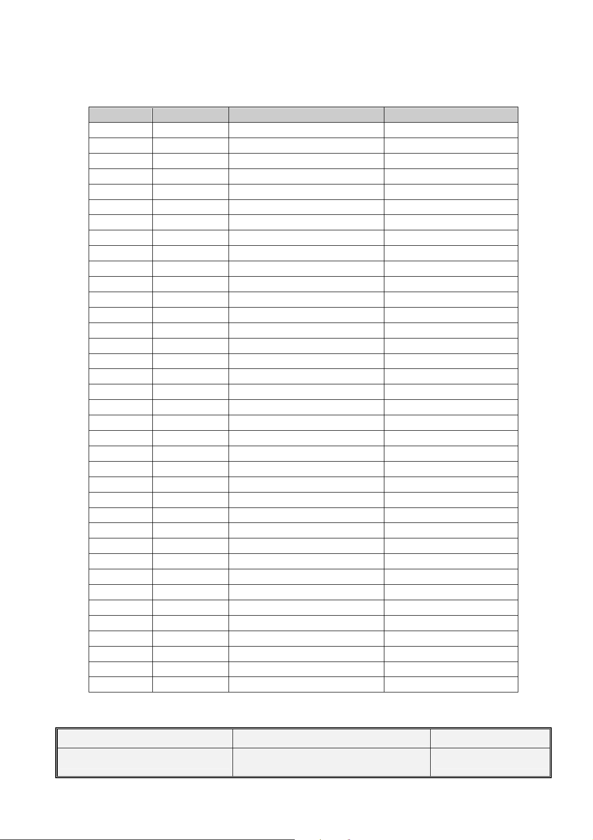
1 List of available level 2,5e parts A60/C60
ID-No Type Name, Location Part-No.
D171 IC Egold+ V3.1F , V3.1H M42 L36197-F5019-F415
D361 IC ASIC D0950 SALZBURG L36145-J4682-Y43
R955 Resistor Temp_Resistor L36120-F4223-H
V181 Diode Diode_Battery_Interface L36702-A1051
V211 Transistor Tran._Vibra L36830-C1097-D670
V220 Diode Diode_Vibra L36851-Z9105-Z981
V222 Transistor Trans_Light_ L36830-C1112-D670
V361 Transistor Tran._Charge L36830-C1110-D670
V951 Diode Capa_Diode L36840-D61-D670
Z171 Quartz Quarz/Egold L36145-F102-Y10
Z211 Filter Logic/IO_Interface L36197-F5000-F116
Z950 Quartz Oszillator_26MHz L36145-F260-Y17
N881 Filter Ant_Switch_Diplexer L36145-K280-Y258
N882 IC Transceiver IC L36820-L6142-D670
N901 IC Power_Amplifier L36851Z2002A 63
R141 Resistor Resistor 0 Ohm L36852-C X
R214 Resistor Resistor 0 Ohm L36852-C X
R215 Resistor Resistor 0 Ohm L36852-C X
R294 Resistor Resistor 0 Ohm L36852-C X
R804 Resistor Resistor 0 Ohm L36852-C X
R884 Resistor Resistor 0 Ohm L36852-C X
R885 Resistor Resistor 0 Ohm L36852-C X
R883 Resistor Resistor 0 Ohm L36852-C X
R950 Resistor Resistor 0 Ohm L36852-C X
V151 Diode Diode KB7 L36840-D5062-D670
C368 Capacitor Capacitor 2U2 L36377-F6225-M
C369 Capacitor Capacitor 2U2 L36377-F6225-M
C370 Capacitor Capacitor 2U2 L36377-F6225-M
C371 Capacitor Capacitor 2U2 L36377-F6225-M
C373 Capacitor Capacitor 2U2 L36377-F6225-M
C377 Capacitor Capacitor 2U2 L36377-F6225-M
C847 Capacitor Capacitor 2U2 L36377-F6225-M
C287 Capacitor Capacitor 2U2 L36377-F6225-M
C288 Capacitor Capacitor 2U2 L36377-F6225-M
C289 Capacitor Capacitor 2U2 L36377-F6225-M
C916 Capacitor Capacitor 2U2 L36377-F6225-M
V 2.1 Page 4 of 61 Com MD CC GRM T
A60/A62/A65/C60/C61/MC60
Company Confidential
Copyright 2004© Siemens AG
12/04
Page 5
s Com
C283 Capacitor Capacitor 1U0 L36377-F6105-K
C284 Capacitor Capacitor 1U0 L36377-F6105-K
C285 Capacitor Capacitor 1U0 L36377-F6105-K
C372 Capacitor Capacitor 1U0 L36377-F6105-K
C286 Capacitor Capacitor 1U0 L36377-F6105-K
C395 Capacitor Capacitor RTC L36392-F1107-M
C165 Capacitor Capacitor 100N L36853-C9104-M4
C200 Capacitor Capacitor 100N L36853-C9104-M4
C201 Capacitor Capacitor 100N L36853-C9104-M4
C202 Capacitor Capacitor 100N L36853-C9104-M4
C207 Capacitor Capacitor 100N L36853-C9104-M4
C209 Capacitor Capacitor 100N L36853-C9104-M4
C220 Capacitor Capacitor 100N L36853-C9104-M4
C362 Capacitor Capacitor 100N L36853-C9104-M4
C363 Capacitor Capacitor 100N L36853-C9104-M4
C364 Capacitor Capacitor 100N L36853-C9104-M4
C365 Capacitor Capacitor 100N L36853-C9104-M4
C366 Capacitor Capacitor 100N L36853-C9104-M4
C367 Capacitor Capacitor 100N L36853-C9104-M4
C374 Capacitor Capacitor 100N L36853-C9104-M4
C381 Capacitor Capacitor 100N L36853-C9104-M4
C382 Capacitor Capacitor 100N L36853-C9104-M4
C383 Capacitor Capacitor 100N L36853-C9104-M4
C384 Capacitor Capacitor 100N L36853-C9104-M4
C385 Capacitor Capacitor 100N L36853-C9104-M4
C386 Capacitor Capacitor 100N L36853-C9104-M4
C800 Capacitor Capacitor 100N L36853-C9104-M4
C814 Capacitor Capacitor 100N L36853-C9104-M4
C820 Capacitor Capacitor 100N L36853-C9104-M4
C821 Capacitor Capacitor 100N L36853-C9104-M4
C956 Capacitor Capacitor 100N L36853-C9104-M4
C912 Capacitor Capacitor 100N L36853-C9104-M4
N280 IC VReg Display_Backlight L36810-C6098-D670
V191 Diode Diode_Sim Interface L36197-F5014-F98
V 2.1 Page 5 of 61 Com MD CC GRM T
A60/A62/A65/C60/C61/MC60
Company Confidential
Copyright 2004© Siemens AG
12/04
Page 6

s Com
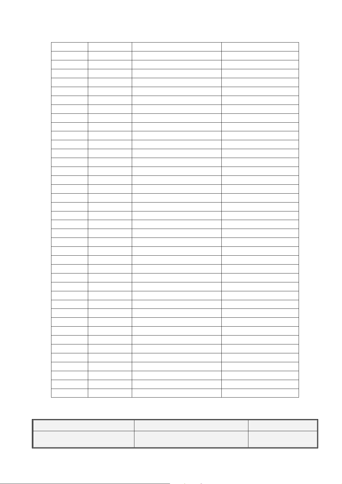
2 List of available level 2,5e parts A62/A65
ID Type Component Details Partnumber
N881 Filter Ant_Switch_Diplexer L36145-K280-Y258
N882 IC Transceiver IC L36820-L6142-D670
Z950 Quartz Oszillator_26MHz L36145-F260-Y17
V951 Diode Capa_Diode L36840-D61-D670
R955 Resistor Temp_Resistor L36120-F4223-H
N901 IC Power_Amplifier L36851-Z2002-A63
D171 IC Egold+ V3.1F , V3.1H M42 L36197-F5019-F415
Z171 Quartz Quarz/Egold L36145-F102-Y10
D361 IC ASIC D0950 SALZBURG L36145-J4682-Y43
V361 Transistor Tran._Charge L36830-C1110-D670
Z211 Filter Logic/IO_Interface L36197-F5000-F116
V211 Transistor Tran._Vibra L36830-C1097-D670
V220 Diode Diode_Vibra L36851-Z9105-Z981
N280 IC VReg Display_Backlight L36810-C6098-D670
V222 Transistor Trans_Light_ L36830-C1112-D670
V191 Diode Diode_Sim Interface L36197-F5014-F98
V151 Diode Diode KB7 L36840-D5062-D670
R141 Resistor Resistor 0 Ohm L36852-C X
R294 Resistor Resistor 0 Ohm L36852-C X
R804 Resistor Resistor 0 Ohm L36852-C X
R884 Resistor Resistor 0 Ohm L36852-C X
R885 Resistor Resistor 0 Ohm L36852-C X
R950 Resistor Resistor 0 Ohm L36852-C X
C369 Capacitor Capacitor 2U2 L36377-F6225-M
C370 Capacitor Capacitor 2U2 L36377-F6225-M
C371 Capacitor Capacitor 2U2 L36377-F6225-M
C373 Capacitor Capacitor 2U2 L36377-F6225-M
C377 Capacitor Capacitor 2U2 L36377-F6225-M
C825 Capacitor Capacitor 2U2 L36377-F6225-M
C287 Capacitor Capacitor 2U2 L36377-F6225-M
C288 Capacitor Capacitor 2U2 L36377-F6225-M
C289 Capacitor Capacitor 2U2 L36377-F6225-M
C916 Capacitor Capacitor 2U2 L36377-F6225-M
C283 Capacitor Capacitor 1U0 L36377-F6105-K
C284 Capacitor Capacitor 1U0 L36377-F6105-K
C285 Capacitor Capacitor 1U0 L36377-F6105-K
C372 Capacitor Capacitor 1U0 L36377-F6105-K
C286 Capacitor Capacitor 1U0 L36377-F6105-K
C395 Capacitor Capacitor RTC L36392-F1107-M
C165 Capacitor Capacitor 100N L36853-C9104-M4
C200 Capacitor Capacitor 100N L36853-C9104-M4
C201 Capacitor Capacitor 100N L36853-C9104-M4
C202 Capacitor Capacitor 100N L36853-C9104-M4
V 2.1 Page 6 of 61 Com MD CC GRM T
A60/A62/A65/C60/C61/MC60
Company Confidential
Copyright 2004© Siemens AG
12/04
Page 7
s Com
C207 Capacitor Capacitor 100N L36853-C9104-M4
C209 Capacitor Capacitor 100N L36853-C9104-M4
C220 Capacitor Capacitor 100N L36853-C9104-M4
C362 Capacitor Capacitor 100N L36853-C9104-M4
C363 Capacitor Capacitor 100N L36853-C9104-M4
C364 Capacitor Capacitor 100N L36853-C9104-M4
C365 Capacitor Capacitor 100N L36853-C9104-M4
C366 Capacitor Capacitor 100N L36853-C9104-M4
C367 Capacitor Capacitor 100N L36853-C9104-M4
C374 Capacitor Capacitor 100N L36853-C9104-M4
C381 Capacitor Capacitor 100N L36853-C9104-M4
C382 Capacitor Capacitor 100N L36853-C9104-M4
C383 Capacitor Capacitor 100N L36853-C9104-M4
C384 Capacitor Capacitor 100N L36853-C9104-M4
C385 Capacitor Capacitor 100N L36853-C9104-M4
C386 Capacitor Capacitor 100N L36853-C9104-M4
C800 Capacitor Capacitor 100N L36853-C9104-M4
C820 Capacitor Capacitor 100N L36853-C9104-M4
C821 Capacitor Capacitor 100N L36853-C9104-M4
C956 Capacitor Capacitor 100N L36853-C9104-M4
C912 Capacitor Capacitor 100N L36853-C9104-M4
V 2.1 Page 7 of 61 Com MD CC GRM T
A60/A62/A65/C60/C61/MC60
Company Confidential
Copyright 2004© Siemens AG
12/04
Page 8
s Com
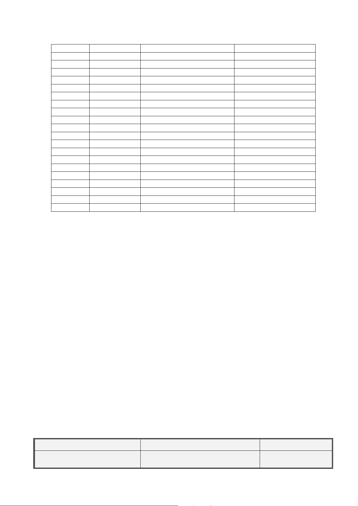
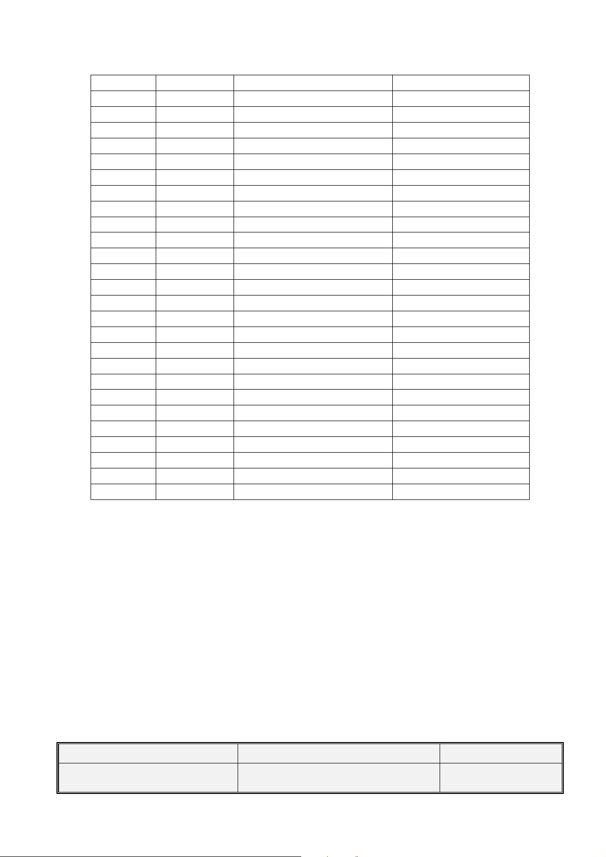
3 List of available level 2,5e parts MC60
ID-No Type Name, Location Part-No.
D171 IC Egold+ V3.1F , V3.1H M42 L36197-F5019-F415
D361 IC ASIC D0950 SALZBURG L36145-J4682-Y43
R959 Resistor Temp_Resistor L36120-F4223-H
V181 Diode Diode_Battery_Interface L36702-A1051
V211 Transistor Tran._Vibra L36830-C1097-D670
V220 Diode Diode_Vibra L36851-Z9105-Z981
V222 Transistor Trans_Light_ L36830-C1112-D670
V361 Transistor Tran._Charge L36830-C1110-D670
V951 Diode Capa_Diode L36840-D61-D670
Z171 Quartz Quarz/Egold L36145-F102-Y10
Z211 Filter Logic/IO_Interface L36197-F5000-F116
Z950 Quartz Oszillator_26MHz L36145-F260-Y17
N881 Filter Ant_Switch_Diplexer L36145-K280-Y258
N882 IC Transceiver IC L36820-L6142-D670
N901 IC Power_Amplifier L36851Z2002A 63
D200 IC Camera ASIC L36820-U6024-D670
D201 IC Camera Interface L36810-B6079-D670
N200 IC Camera Powersupply L36810-C6134-D670
R141 Resistor Resistor 0 Ohm L36852-C X
R160 Resistor Resistor 0 Ohm L36852-C X
R250 Resistor Resistor 0 Ohm L36852-C X
R251 Resistor Resistor 0 Ohm L36852-C X
R214 Resistor Resistor 0 Ohm L36852-C X
R215 Resistor Resistor 0 Ohm L36852-C X
R217 Resistor Resistor 0 Ohm L36852-C X
R294 Resistor Resistor 0 Ohm L36852-C X
R804 Resistor Resistor 0 Ohm L36852-C X
R253 Resistor Resistor 0 Ohm L36852-C X
R201 Resistor Resistor 0 Ohm L36852-C X
R254 Resistor Resistor 0 Ohm L36852-C X
R224 Resistor Resistor 0 Ohm L36852-C X
R255 Resistor Resistor 0 Ohm L36852-C X
R908 Resistor Resistor 0 Ohm L36852-C X
R256 Resistor Resistor 0 Ohm L36852-C X
R257 Resistor Resistor 0 Ohm L36852-C X
R258 Resistor Resistor 0 Ohm L36852-C X
R232 Resistor Resistor 0 Ohm L36852-C X
V 2.1 Page 8 of 61 Com MD CC GRM T
A60/A62/A65/C60/C61/MC60
Company Confidential
Copyright 2004© Siemens AG
12/04
Page 9
s Com
R884 Resistor Resistor 0 Ohm L36852-C X
R885 Resistor Resistor 0 Ohm L36852-C X
R259 Resistor Resistor 0 Ohm L36852-C X
R271 Resistor Resistor 0 Ohm L36852-C X
R273 Resistor Resistor 0 Ohm L36852-C X
R274 Resistor Resistor 0 Ohm L36852-C X
R275 Resistor Resistor 0 Ohm L36852-C X
R276 Resistor Resistor 0 Ohm L36852-C X
V151 Diode Diode KB7 L36840-D5062-D670
L361 Diode Cam Sensor L36840-D5062D670
C368 Capacitor Capacitor 2U2 L36377-F6225-M
C369 Capacitor Capacitor 2U2 L36377-F6225-M
C370 Capacitor Capacitor 2U2 L36377-F6225-M
C371 Capacitor Capacitor 2U2 L36377-F6225-M
C373 Capacitor Capacitor 2U2 L36377-F6225-M
C377 Capacitor Capacitor 2U2 L36377-F6225-M
C219 Capacitor Capacitor 2U2 L36377-F6225-M
C847 Capacitor Capacitor 2U2 L36377-F6225-M
C287 Capacitor Capacitor 2U2 L36377-F6225-M
C288 Capacitor Capacitor 2U2 L36377-F6225-M
C289 Capacitor Capacitor 2U2 L36377-F6225-M
C916 Capacitor Capacitor 2U2 L36377-F6225-M
C283 Capacitor Capacitor 1U0 L36377-F6105-K
C284 Capacitor Capacitor 1U0 L36377-F6105-K
C285 Capacitor Capacitor 1U0 L36377-F6105-K
C372 Capacitor Capacitor 1U0 L36377-F6105-K
C286 Capacitor Capacitor 1U0 L36377-F6105-K
C395 Capacitor Capacitor RTC L36392-F1107-M
C165 Capacitor Capacitor 100N L36853-C9104-M4
C200 Capacitor Capacitor 100N L36853-C9104-M4
C201 Capacitor Capacitor 100N L36853-C9104-M4
C202 Capacitor Capacitor 100N L36853-C9104-M4
C203 Capacitor Capacitor 100N L36853-C9104-M4
C204 Capacitor Capacitor 100N L36853-C9104-M4
C207 Capacitor Capacitor 100N L36853-C9104-M4
C209 Capacitor Capacitor 100N L36853-C9104-M4
C220 Capacitor Capacitor 100N L36853-C9104-M4
C230 Capacitor Capacitor 100N L36853-C9104-M4
C231 Capacitor Capacitor 100N L36853-C9104-M4
C232 Capacitor Capacitor 100N L36853-C9104-M4
V 2.1 Page 9 of 61 Com MD CC GRM T
A60/A62/A65/C60/C61/MC60
Company Confidential
Copyright 2004© Siemens AG
12/04
Page 10
s Com
C233 Capacitor Capacitor 100N L36853-C9104-M4
C234 Capacitor Capacitor 100N L36853-C9104-M4
C362 Capacitor Capacitor 100N L36853-C9104-M4
C363 Capacitor Capacitor 100N L36853-C9104-M4
C364 Capacitor Capacitor 100N L36853-C9104-M4
C365 Capacitor Capacitor 100N L36853-C9104-M4
C366 Capacitor Capacitor 100N L36853-C9104-M4
C367 Capacitor Capacitor 100N L36853-C9104-M4
C374 Capacitor Capacitor 100N L36853-C9104-M4
C381 Capacitor Capacitor 100N L36853-C9104-M4
C382 Capacitor Capacitor 100N L36853-C9104-M4
C383 Capacitor Capacitor 100N L36853-C9104-M4
C384 Capacitor Capacitor 100N L36853-C9104-M4
C385 Capacitor Capacitor 100N L36853-C9104-M4
C386 Capacitor Capacitor 100N L36853-C9104-M4
C800 Capacitor Capacitor 100N L36853-C9104-M4
C814 Capacitor Capacitor 100N L36853-C9104-M4
C820 Capacitor Capacitor 100N L36853-C9104-M4
C821 Capacitor Capacitor 100N L36853-C9104-M4
C956 Capacitor Capacitor 100N L36853-C9104-M4
C235 Capacitor Capacitor 100N L36853-C9104-M4
C229 Capacitor Capacitor 100N L36853-C9104-M4
C803 Capacitor Capacitor 100N L36853-C9104-M4
C809 Capacitor Capacitor 100N L36853-C9104-M4
C912 Capacitor Capacitor 100N L36853-C9104-M4
N280 IC VReg Display_Backlight L36810-C6098-D670
V191 Diode Diode_Sim Interface L36197-F5014-F98
V 2.1 Page 10 of 61 Com MD CC GRM T
A60/A62/A65/C60/C61/MC60
Company Confidential
Copyright 2004© Siemens AG
12/04
Page 11
s Com
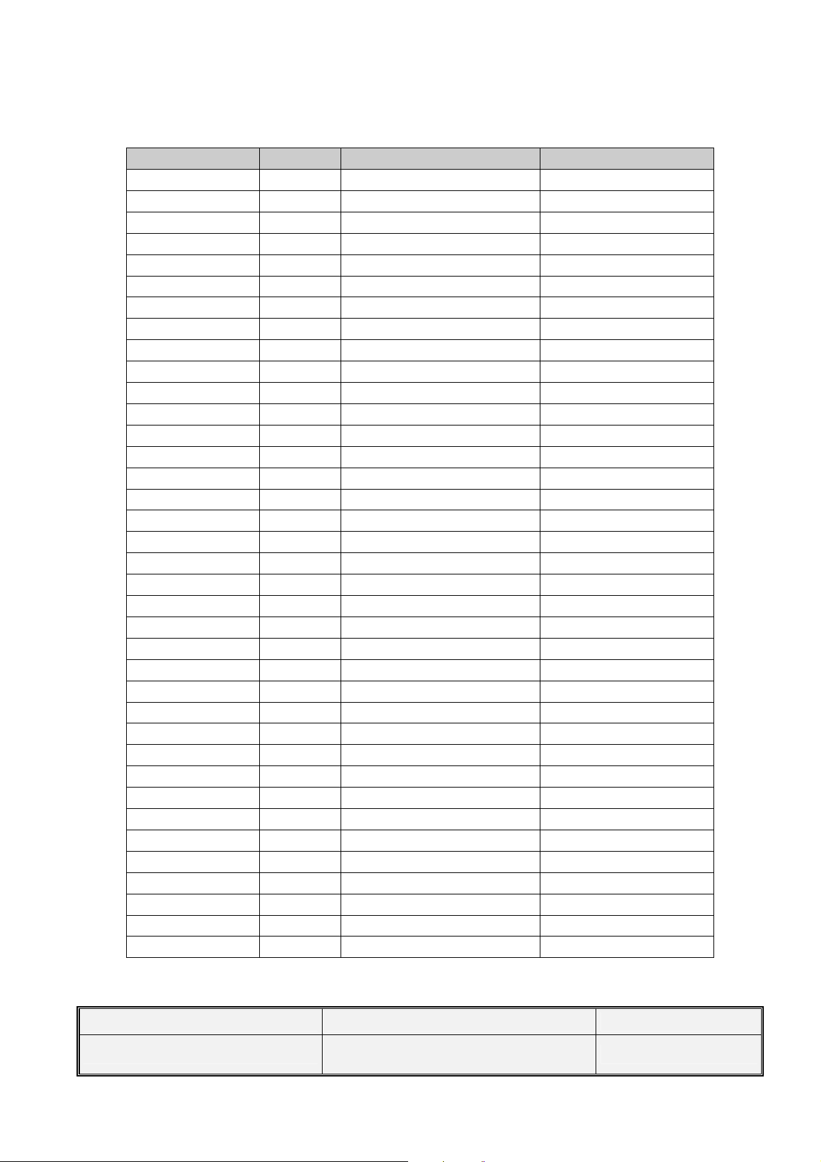
4 List of available level 2,5e parts C61
No Type Name, Location Part-No.
D171 IC Egold+ V3.1F , V3.1H M42 L36197-F5019-F415
D361 IC ASIC D0950 SALZBURG L36145-J4682-Y43
R955 Resistor Temp_Resistor L36120-F4223-H
V181 Diode Diode_Battery_Interface L36702-A1051
V211 Transistor Tran._Vibra L36830-C1097-D670
V220 Diode Diode_Vibra L36851-Z9105-Z981
V222 Transistor Trans_Light_ L36830-C1112-D670
V361 Transistor Tran._Charge L36830-C1110-D670
V951 Diode Capa_Diode L36840-D61-D670
Z171 Quartz Quarz/Egold L36145-F102-Y10
Z211 Filter Logic/IO_Interface L36197-F5000-F116
Z950 Quartz Oszillator_26MHz L36145-F260-Y17
N880 Filter Ant_Switch_Diplexer FEM L36145-K280-Y259
N882 IC Transceiver IC L36820-L6142-D670
N901 IC Power_Amplifier L36851-Z2002-A63
R141 Resistor Resistor 0 Ohm L36852-C X
R214 Resistor Resistor 0 Ohm L36852-C X
R215 Resistor Resistor 0 Ohm L36852-C X
R294 Resistor Resistor 0 Ohm L36852-C X
R804 Resistor Resistor 0 Ohm L36852-C X
R884 Resistor Resistor 0 Ohm L36852-C X
R885 Resistor Resistor 0 Ohm L36852-C X
R950 Resistor Resistor 0 Ohm L36852-C X
V151 Diode Diode KB7 L36840-D5062-D670
C368 Capacitor Capacitor 2U2 L36377-F6225-M
C369 Capacitor Capacitor 2U2 L36377-F6225-M
C370 Capacitor Capacitor 2U2 L36377-F6225-M
C371 Capacitor Capacitor 2U2 L36377-F6225-M
C373 Capacitor Capacitor 2U2 L36377-F6225-M
C377 Capacitor Capacitor 2U2 L36377-F6225-M
C847 Capacitor Capacitor 2U2 L36377-F6225-M
C287 Capacitor Capacitor 2U2 L36377-F6225-M
C288 Capacitor Capacitor 2U2 L36377-F6225-M
C289 Capacitor Capacitor 2U2 L36377-F6225-M
C916 Capacitor Capacitor 2U2 L36377-F6225-M
C283 Capacitor Capacitor 1U0 L36377-F6105-K
C284 Capacitor Capacitor 1U0 L36377-F6105-K
V 2.1 Page 11 of 61 Com MD CC GRM T
A60/A62/A65/C60/C61/MC60
Company Confidential
Copyright 2004© Siemens AG
12/04
Page 12
s Com
C285 Capacitor Capacitor 1U0 L36377-F6105-K
C372 Capacitor Capacitor 1U0 L36377-F6105-K
C286 Capacitor Capacitor 1U0 L36377-F6105-K
C395 Capacitor Capacitor RTC L36392-F1107-M
C165 Capacitor Capacitor 100N L36853-C9104-M4
C200 Capacitor Capacitor 100N L36853-C9104-M4
C201 Capacitor Capacitor 100N L36853-C9104-M4
C202 Capacitor Capacitor 100N L36853-C9104-M4
C207 Capacitor Capacitor 100N L36853-C9104-M4
C209 Capacitor Capacitor 100N L36853-C9104-M4
C220 Capacitor Capacitor 100N L36853-C9104-M4
C362 Capacitor Capacitor 100N L36853-C9104-M4
C363 Capacitor Capacitor 100N L36853-C9104-M4
C364 Capacitor Capacitor 100N L36853-C9104-M4
C365 Capacitor Capacitor 100N L36853-C9104-M4
C366 Capacitor Capacitor 100N L36853-C9104-M4
C367 Capacitor Capacitor 100N L36853-C9104-M4
C374 Capacitor Capacitor 100N L36853-C9104-M4
C381 Capacitor Capacitor 100N L36853-C9104-M4
C382 Capacitor Capacitor 100N L36853-C9104-M4
C383 Capacitor Capacitor 100N L36853-C9104-M4
C384 Capacitor Capacitor 100N L36853-C9104-M4
C385 Capacitor Capacitor 100N L36853-C9104-M4
C386 Capacitor Capacitor 100N L36853-C9104-M4
C800 Capacitor Capacitor 100N L36853-C9104-M4
C814 Capacitor Capacitor 100N L36853-C9104-M4
C820 Capacitor Capacitor 100N L36853-C9104-M4
C821 Capacitor Capacitor 100N L36853-C9104-M4
C956 Capacitor Capacitor 100N L36853-C9104-M4
C912 Capacitor Capacitor 100N L36853-C9104-M4
N280 IC VReg Display_Backlight L36810-C6098-D670
V191 Diode Diode_Sim Interface L36197-F5014-F98
V 2.1 Page 12 of 61 Com MD CC GRM T
A60/A62/A65/C60/C61/MC60
Company Confidential
Copyright 2004© Siemens AG
12/04
Page 13

s Com
5 Required Equipment for Level 2,5e
- GSM-Tester (CMU200 or 4400S incl. Options)
- PC-incl. Monitor, Keyboard and Mouse
- Bootadapter 2000/2002 (L36880-N9241-A200)
- Adapter cable for Bootadapter due to new Lumberg connector (F30032-P226-A1)
- Troubleshooting Frame A60/C60/C61/MC60 (F30032-P307-A1)
- Troubleshooting Frame A62/A65 (F30032-P405-A1)
- Power Supply NGMO1/NGMO2
- Spectrum Analyser
- Active RF-Probe incl. Power Supply
- Oscilloscope incl. Probe
- RF-Connector (N<>SMA(f))
- Power Supply Cables
- Dongle (F30032-P28-A1) if USB-Dongle is used a special driver for NT is required
- BGA Soldering equipment
Reference: Equipment recommendation V1.4
(downloadable from the technical support page)
6 Required Software for Level 2,5e
- Windows NT Version4
- Winsui version1.45 or higher
- Software for GSM-Tester ( Cats(Acterna/Wiltek) or CMU-GO(Rohde&Schwarz) )
- Software for reference oscillator adjustment
- Internet unblocking solution (JPICS)
- Dongle driver for USB-Dongle if used with WIN NT4
V 2.1 Page 13 of 61 Com MD CC GRM T
A60/A62/A65/C60/C61/MC60
Company Confidential
Copyright 2004© Siemens AG
12/04
Page 14

s Com
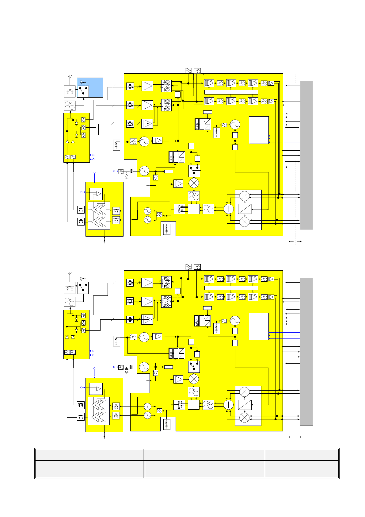
7 Radio Part
The radio part realizes the conversion of the GMSK-HF-signals from the antenna to the baseband and vice versa.
In the receiving direction, the signals are split in the I- and Q-component and led to the D/Aconverter of the logic part. In the transmission direction, the GMSK-signal is generated in an
Up Conversion Modulation Phase Locked Loop by modulation of the I- and Q-signals which
were generated in the logic part. After that the signals are amplified in the power amplifier.
Transmitter and Receiver are never active at the same time. Simultaneous receiving in two
bands is impossible. Simultaneous transmission in two bands is impossible, too. However the
monitoring band (monitoring timeslot) in the TDMA-frame can be chosen independently of the
receiving respectively the transmitting band (RX- and TX timeslot of the band).
The RF-part of the A60/A62/A65/C60/MC60 is dimensioned for triple band operation
(EGSM900, GSM1800, GSM1900) supporting GPRS functionality up to multiclass 8. C61 is
dimensioned for dual band operation (GSM850, GSM1900) supporting GPRS functionality up
to multiclass 8.
The RF-circuit consists of the following components:
• Hitachi Bright VE chip set with the following functionality:
o PLL for local oscillator LO1 and LO2 and TxVCO
o Integrated local oscillators LO1, LO2 (without loop filter)
o Integrated TxVCO (without loop filter and core inductors for GSM)
o Direct conversion receiver including LNA, DC-mixer, channel filtering and PGC-
amplifier
o Active part of 26 MHz reference oscillator
• Hitachi LTCC transmitter power amplifier with integrated power control circuitry
• Hitachi Frontend-Module including RX-/TX-switch and EGSM900 / GSM1800 / GSM 1900
receiver SAW-filters for A60/C60/MC60
• Hitachi Frontend-Module including RX-/TX-switch and GSM850 / GSM 1900 receiver
SAW-filters for C61
Quartz and passive circuitry of the 26MHz VCXO reference oscillator.
V 2.1 Page 14 of 61 Com MD CC GRM T
A60/A62/A65/C60/C61/MC60
Company Confidential
Copyright 2004© Siemens AG
12/04
Page 15
s Com
g
7.1 Block diagram RF part
A60/A62/A65/C60/MC60
antenna
matching
FEM
Hitachi
internal
antenna
RF Block Diagram
only MC60
external
antenna
mechanical
antenna
925-960 MHz
switch
1805 - 1880 MHz
1930 - 1990 MHz
2
FEM incl.
SAW &
PIN-diode
switch
PA_RAMP
TXONPA
BATT+
external
Loopfilter
TXON_GSM
RF_SW
Hitachi
PA
Internal power
control using
"current sensing"
Vapc
2
2
AFC_PNM
Varicap
Crystal
26MHz
to Baseband
2
GSM LNA
2
2
PCS LNA
integr. RF VCO
3476 - 3980
MHz
VCXO
26 MHz
26MHz
1800/1900
Integrated
TX-VCOs
PCN LNA
900
frontend
IQ demodulator
IQ demodulator
RF PLL
TX-loop
filter
1
1
26MHz
2
2
PFD
CP
+
1/2
1/2
D
1
R
1
PCN GSM
+
PD
phase
charge
detector
pump
Transceiver IC
Hitachi Bright VE
CP
1/2
IF PLL
+
PFD
26MHz
R
1
D
1
Analouge /
Digital Phase -
frequency
detector
Feedback filter
DC autocalibration
640 - 656 MHz
external
loopfilter
GSM: 80MHz
PCN: 80MHz
DCS: 80MHz
integr.
IF VCO
1/2
1/2
IQ modulator
BATT+
VCC2_8
VCC_SYN
BANDSW
PA_RAMP
State
machine
Serial
Interface
TX_GSM
TX_PCN
TXONPA
RFCLK
RFSTR
RFDATA
26_MHz_BB
26_MHz_BT
TVCXO
AFC_PNM
RF_I
RF_IX
Basebend
1
2
RF_Q
RF_QX
base bandradio part
C61
RF Block Dia
internal
antenna
antenna
matching
FEM
Hitachi
FEM incl.
SAW &
PIN-diode
switch
PA_RAMP
TXONPA
external
Loopfilter
TXON_GSM
RF_SW
BATT+
ram
869-894 MHz
1930 - 1990 MHz
2
PA
Hitachi
Internal power
control using
"current sensing"
Vapc
2
AFC_PNM
Varicap
Crystal
26MHz
to Baseband
2
GSM LNA
2
PCN LNA
2
PCS LNA
integr. RF VCO
VCXO
26 MHz
26MHz
850
1900
Integrated
TX-VCOs
frontend
IQ demodulator
IQ demodulator
RF PLL
TX-loop
1
1
26MHz
filter
2
2
PFD+CP
1/2
1/2
D
1
R
1
PCS GSM
+
PD
phase
charge
detector
pump
Transceiver IC
Hitachi Bright VE
1/2
IF PLL
PFD+CP
26MHz
R
1
D
1
Analouge /
Digital Phase -
frequency
detector
Feedback filter
DC autocalibration
640 - 656 MHz
external
loopfilter
GSM: 80MHz
PCN: 80MHz
DCS: 80MHz
integr.
IF VCO
1/2
1/2
IQ modulator
BATT+
VCC2_8
VCC_SYN
BANDSW
PA_RAMP
State
machine
Serial
Interface
TX_GSM
TX_PCN
TXONPA
RFCLK
RFSTR
RFDATA
26_MHz_BB
26_MHz_BT
TVCXO
AFC_PNM
RF_I
RF_IX
Basebend
1
2
RF_Q
RF_QX
base bandradio part
V 2.1 Page 15 of 61 Com MD CC GRM T
A60/A62/A65/C60/C61/MC60
Company Confidential
Copyright 2004© Siemens AG
12/04
Page 16
s Com
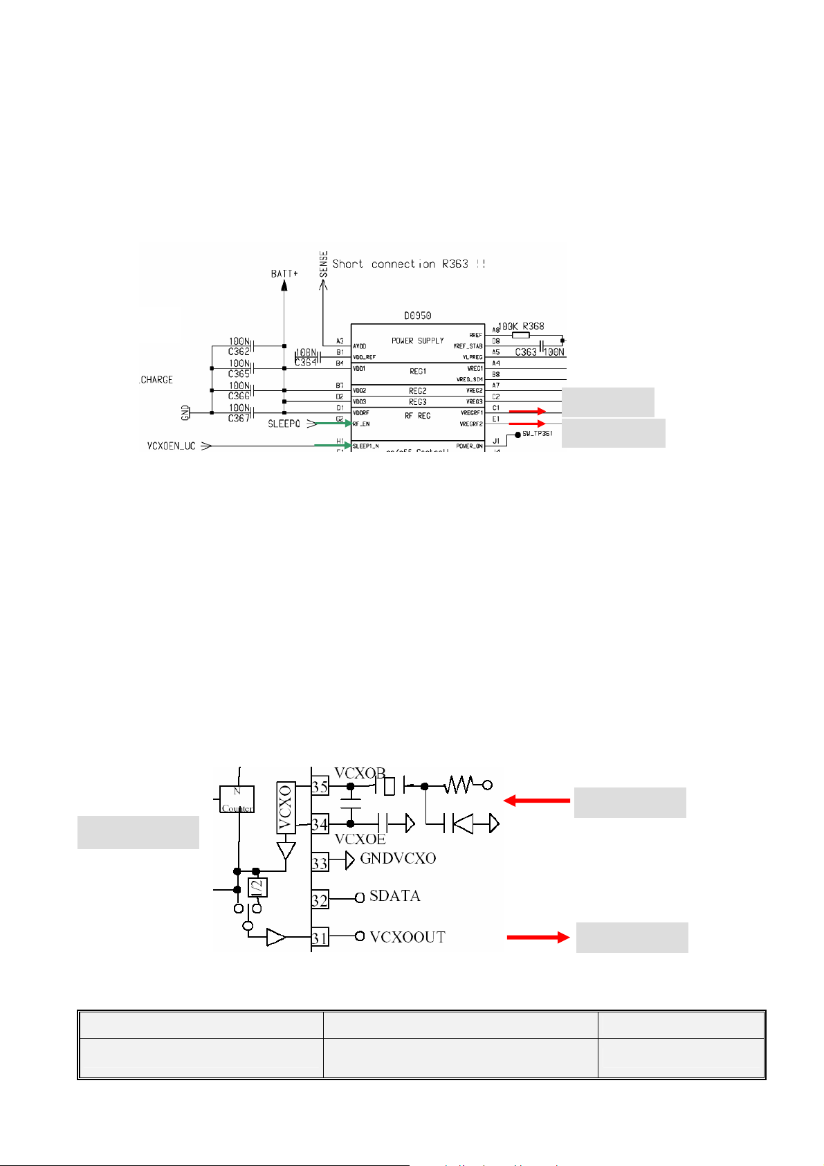
7.2 Power Supply RF-Part
The voltage regulator for the RF-part is located inside the ASIC D361.(see chapter 5.2).It generates
the required 2,8V “RF-Voltages” named VCC2_8 and VCC_SYN . The voltage regulator is activated
as well as deactivated via SLEEPQ
EGOLD+. The temporary deactivation is used to extend the stand by time.
Circuit diagram
(TDMA-Timer H16) and VCXOEN_UC (Miscellaneous R6) provided by the
VCC2_8
VCC_SYN
7.3 Frequency generation
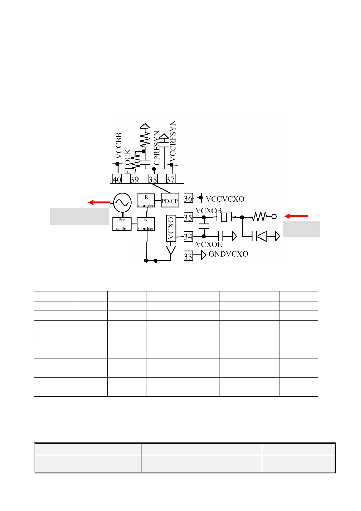
7.3.1 Synthesizer: The discrete VCXO (26MHz)
The A60/A62/A65/C60/C61/MC60 mobile is using a reference frequency of 26MHz. The generation of
the 26MHz signal is done via a VCXO. This oscillator consists mainly of:
A 26MHz crystal Z950
A capacity diode V951
TP (test point) of the 26MHz signal is the TP 820
The oscillator output signal 26MHz_RF is directly connected to the BRIGHT IC (pin 35) to be used as
reference frequency inside the Bright (PLL). The signal leaves the Bright IC as BB_SIN26M (pin 31)
to be further used from the EGOLD+ (D171
Bright VE
(functional T3)).
VCXO Out
EGOLD In
V 2.1 Page 16 of 61 Com MD CC GRM T
A60/A62/A65/C60/C61/MC60
Company Confidential
Copyright 2004© Siemens AG
12/04
Page 17
s Com
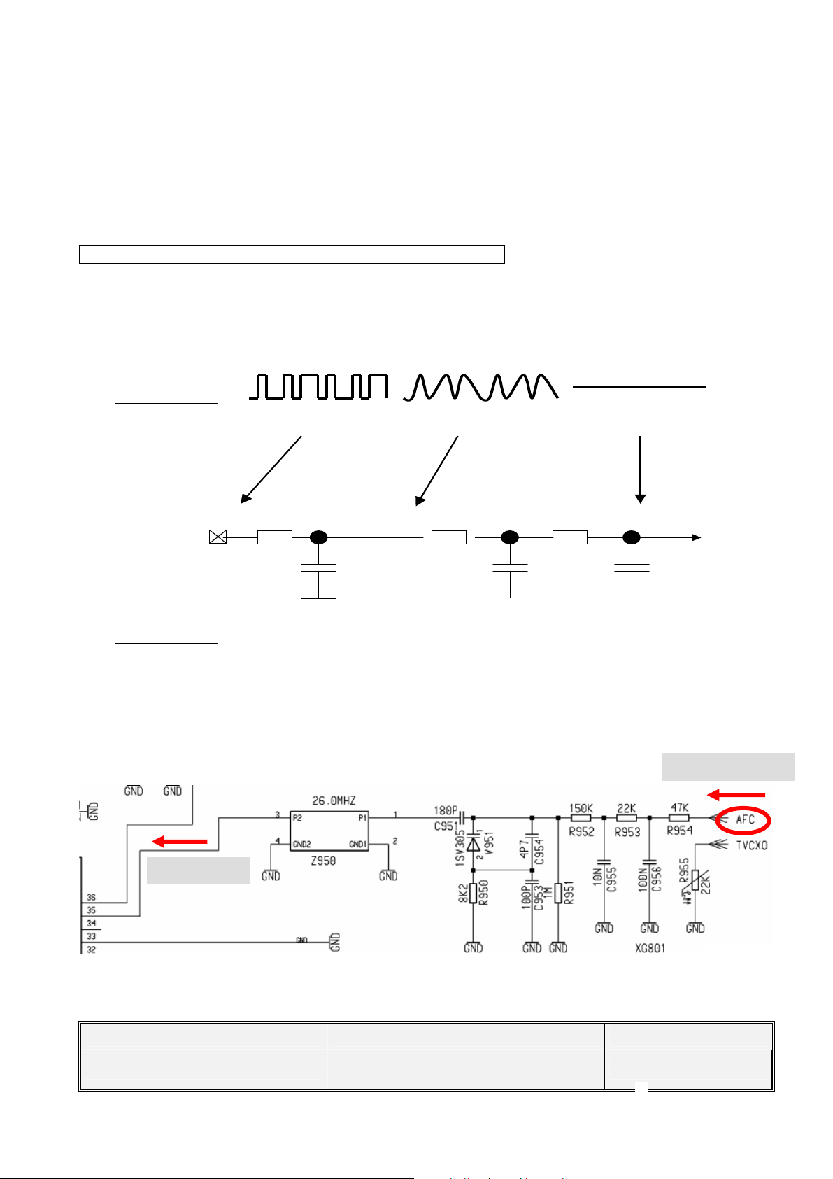
To compensate frequency drifts (e.g. caused by temperature) the oscillator frequency is controlled by
the (AFC) signal, generated through the internal EGOLD+ (D100
diode V951. Reference for the “EGOLD-PLL” is the base station frequency received via the
Frequency Correction Burst. To compensate a temperature caused frequency drift, the temperaturedepending resistor R955 is placed near the VCXO to measure the temperature. The measurement
result TVCXO is reported to the EGOLD+
The required voltage VCC_SYN is provided by the ASCI D361
Waveform of the AFC_PNM signal from EGOLD+ to Oscillator
(Analog Interface P3) via R138 as the signal TENV.
(functional U5)) PLL via the capacity
Signalform
EGOLD+
1 2 3
AFC
Circuit diagram
to BRIGHT
1
R158
30K 22K
AFC_PNM
C165
GND
100N
2
R954
47K
C956
GND
R953
100N
C955
3
10N
GND
from EGOLD+
V 2.1 Page 17 of 61 Com MD CC GRM T
A60/A62/A65/C60/C61/MC60
Company Confidential
Copyright 2004© Siemens AG
12/04
Page 18
s Com
7.3.2 Synthesizer: LO1
The first local oscillator (LO1) consists of a PLL and VCO inside Bright (N882) and an external
loop filter The first local oscillator is needed to generate frequencies which enable the
transceiver IC to demodulate the receiver signal and to perform the channel selection in the
TX part. To do so, a control voltage for the LO1 is used, gained by a comparator. This control
voltage is a result of the comparison of the divided LO1 and the 26MHz reference Signal. The
division ratio of the dividers is programmed by the EGOLD+, according to the network
channel requirements.
Matrix to calculate the TX and RX frequencies A60/A62/A65/C60/MC60:
Band RX / TX Channels RF frequencies LO1 frequency IF freq.
EGSM 900 Receive: 0..124 935,0 - 959,8 MHz LO1 = 4*RF
EGSM 900 Transmit: 0..124 890,0 - 914,8 MHz LO1 = 4*(RF+IF) 80,0 MHz
EGSM 900 Receive: 975..1023 925,2 - 934,8 MHz LO1 = 4*RF
EGSM 900 Transmit: 975..1023 880,2 - 889,8 MHz LO1 = 4*(RF+IF) 82,0 MHz
GSM 1800 Receive: 512..661 1805,2 - 1835,0 MHz LO1 = 2*RF
GSM 1800 Transmit: 512..661 1710,2 - 1740,0 MHz LO1 = 2*(RF+IF) 80,0 MHz
GSM 1800 Receive: 661..885 1835,0 - 1879,8 MHz LO1 = 2*RF
GSM 1800 Transmit: 661..885 1740,0 - 1784,8 MHz LO1 = 2*(RF+IF) 82,0 MHz
GSM 1900 Receive: 512..810 1930,2 - 1989,8 MHz LO1 = 2*RF
GSM 1900 Transmit: 512..810 1850,2 - 1909,8 MHz LO1 = 2*(RF+IF) 80,0 MHz
LO1 Output
26MHz
V 2.1 Page 18 of 61 Com MD CC GRM T
A60/A62/A65/C60/C61/MC60
Company Confidential
Copyright 2004© Siemens AG
12/04
Page 19
s Com
Matrix to calculate the TX and RX frequencies C61:
Band RX / TX Channels RF frequencies LO1 frequency IF freq.
GSM 850 Receive: 128..251 869,2 - 893,8 MHz LO1 = 4*RF
GSM 850 Transmit: 128..251 824,2 - 848,8 MHz LO1 = 4*(RF+IF) 80,0 MHz
GSM 1900 Receive: 512..810 1930,2 - 1989,8 MHz LO1 = 2*RF
GSM 1900 Transmit: 512..810 1850,2 - 1909,8 MHz LO1 = 2*(RF+IF) 80,0 MHz
The required voltage VCC_SYN is provided by the ASIC D361.
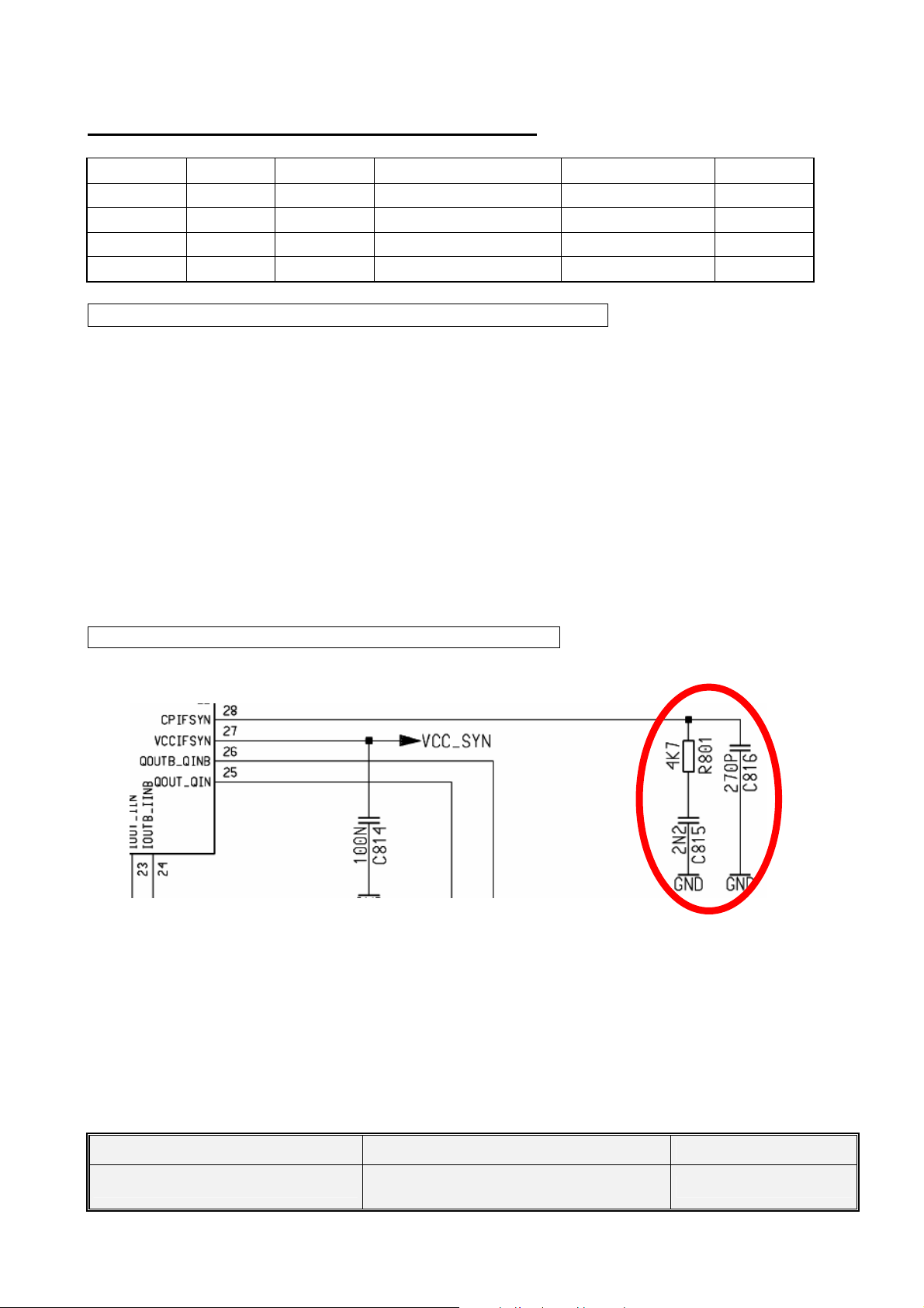
7.3.3 Synthesizer: LO2
The second local oscillator (LO2) consists of a PLL and a VCO which are integrated in Bright
and a second order loopfilter which is realized external (R801; C815; C816). Due to the
direct conversion receiver architecture, the LO2 is only used for transmit-operation. The LO2
covers a frequency range of at least 16 MHz (640MHz – 656MHz).
Before the LO2-signal gets to the modulator it is divided by 8. So the resulting TX-IF
frequencies are 80/82 MHz (dependent on the channel and band). The LO2 PLL and powerup of the VCO is controlled via the tree-wire-bus of Bright (EGOLD+ signals RFDATA;
RFCLK; RFSTR). To ensure the frequency stability, the 640MHz VCO signal is compared by
the phase detector of the 2
signal passes the external loop filter and is used to control the 640/656MHz VCO.
The required voltage VCC_SYN is provided by the ASIC D361
Circuit diagram
nd
PLL with the 26Mhz reference signal. The resulting control
Loop-filter LO2
V 2.1 Page 19 of 61 Com MD CC GRM T
A60/A62/A65/C60/C61/MC60
Company Confidential
Copyright 2004© Siemens AG
12/04
Page 20

s Com
7.3.4 Synthesizer: PLL
The frequency-step is 400 kHz in GSM1800/GSM1900 mode and 800kHz in
GSM850/EGSM900 mode due to the internal divider by two for GSM1800/GSM19000 and
divider by four for GSM850/EGSM900. To achieve the required settling-time in GPRS
operation, the PLL can operate in fastlock-mode a certain period after programming to
ensure a fast settling. After this the loopfilter and currents are switched into normal-mode to
get the necessary phasenoise-performance. The PLL is controlled via the tree-wire-bus of
Bright.
7.4 Antenna switch (electrical/mechanical only C61/MC60)
Internal/External <> Receiver/Transmitter
The C61/MC60 mobile have two antenna switches. A60/A62/A65 and C60 have no external
antenna connector/mechanical antenna switch.
a) The mechanical antenna switch for the differentiation between the internal and
external antenna
b) The electrical antenna switch, for the differentiation between the receiving and
transmitting signals.
To activate the correct settings of this diplexer, the EGOLD+ signals RF_SW and
TXON_GSM are required
MC60 has an integrated “SAR detection” circuit. This circuit is used to decide if the internal
antenna or an external antenna is used. The goal is, to reduce the transmit power when the
internal antenna is used and the mobile is held very close to the body. On the other hand, the
mobile can send with more power, if the external antenna is used. This distinction is done by
the SAR detection circuit which consists of the voltage divider R872 and R873. The
ANT_DET output provides a high level when the external antenna is used. ANT_DET
Interface L16)
is connected to the EGOLD+
Internal/External antenna switch (example MC60)
to / from diplexer
to EGOLD
Internal
(Serial
V 2.1 Page 20 of 61 Com MD CC GRM T
A60/A62/A65/C60/C61/MC60
Company Confidential
Copyright 2004© Siemens AG
12/04
Page 21

s Com
The electrical antenna switch A60/A62/A65/C60/MC60
from PA
to Bright
The electrical antenna switch C61
from PA
to Bright
V 2.1 Page 21 of 61 Com MD CC GRM T
A60/A62/A65/C60/C61/MC60
Company Confidential
Copyright 2004© Siemens AG
12/04
Page 22

s Com
Top View N880/N881
Switching Matrix N880/N881
Pin assignment N880 Pin assignment N881
V 2.1 Page 22 of 61 Com MD CC GRM T
A60/A62/A65/C60/C61/MC60
Company Confidential
Copyright 2004© Siemens AG
12/04
Page 23

s Com
7.5 Receiver
Receiver: Filter to Demodulator
The band filters are located inside the frontend module (N880/N881). The filters are centred
to the band frequencies. The symmetrical filter output is matched to the LNA input of the
Bright (N882).The Bright VE incorporates three RF LNAs for GSM850/EGSM900, GSM1800
and GSM1900 operation. The LNA/mixer can be switched in High- and Low-mode to perform
an amplification of ~ 20dB. For the “High Gain“ state the mixers are optimised to conversion
gain and noise figure, in the “Low Gain“ state the mixers are optimised to large-signal
behavior for operation at a high input level. The Bright performs a direct conversion mixers
which are IQ-demodulators. For the demodulation of the received GSM signals the LO1 is
required. The channel depending LO1 frequencies for 1800MHz/1900MHz bands are divided
by 2 and by 4 for 850MHG/900MHz band. Furthermore the IC includes a programmable gain
baseband amplifier PGA (90 dB range, 2dB steps) with automatic DC-offset calibration. LNA
and PGA are controlled via EGOLD+ signals RFDATA; RFCLK; RFSTR
The channel-filtering is realized inside the chip with a three stage baseband filter for both IQ
chains. Only two capacitors which are part of the first passive RC-filters are external. The
second and third filters are active filters and are fully integrated. The IQ receive signals are
fed into the A/D converters in the EGAIM part of EGOLD+. The post-switched logic measures
the level of the demodulated baseband signal and regulates the level to a defined value by
varying the PGA amplification and switching the appropriate LNA gains.
From the antenna switch, up to the demodulator the received signal passes the following
blocks to get the demodulated baseband signals for the EGOLD+:
Filter
LNA
Demodulator
PGC
N880/N881 Bright(N882)
The required voltage VCC_SYN is provided by the ASIC D361
(RF Control J15, J16, J17).
V 2.1 Page 23 of 61 Com MD CC GRM T
A60/A62/A65/C60/C61/MC60
Company Confidential
Copyright 2004© Siemens AG
12/04
Page 24

s Com
7.6 Transmitter
7.6.1 Transmitter: Modulator and Up-conversion Loop
Transmitter
Up conversion loop
The generation of the GMSK-modulated signal in Bright (N882) is based on the principle of
up conversion modulation phase locked loop. The incoming IQ-signals from the baseband
are mixed with the divided LO2-signal. The modulator is followed by a lowpass filter (corner
frequency ~80 MHz) which is necessary to attenuate RF harmonics generated by the
modulator. A similar filter is used in the feedback-path of the down conversion mixer.
With help of an offset PLL the IF-signal becomes the modulated signal at the final transmit
frequency. Therefore the GMSK modulated rf-signal at the output of the TX-VCOs is mixed
with the divided LO1-signal to a IF-signal and sent to the phase detector. The I/Q modulated
signal with a center frequency of the intermediate frequency is send to the phase detector as
well.
The output signal of the phase detector controls the TxVCO and is processed by a loop filter
whose components are external to the Bright. The TxVCO which is realized inside the Bright
chip generates the GSMK modulated frequency.
Modulator
Bright(N882) R800/C801/C802
The required voltage VCC_SYN is provided by the ASIC D361
Filter
PD Filter
TxVCO
V 2.1 Page 24 of 61 Com MD CC GRM T
A60/A62/A65/C60/C61/MC60
Company Confidential
Copyright 2004© Siemens AG
12/04
Page 25

s Com
A
Circuit diagram
from
antenna
Loop-filter TxVCO
to P
progr. signals
from/to EGOLD+
V 2.1 Page 25 of 61 Com MD CC GRM T
A60/A62/A65/C60/C61/MC60
Company Confidential
Copyright 2004© Siemens AG
12/04
Page 26

s Com
7.7 Bright IC Overview
BRIGHT VE
IC Overview
IC Top View
V 2.1 Page 26 of 61 Com MD CC GRM T
A60/A62/A65/C60/C61/MC60
Company Confidential
Copyright 2004© Siemens AG
12/04
Page 27

s Com
7.7.1 Transmitter: Power Amplifier
The output signals (PCN_PA_IN , and GSM_PA_IN) from the TxVCO are led to the power
amplifier. The power amplifier is a PA-module N901 from Hitachi. It contains two separate 3stage amplifier chains GSM850/EGSM900 and GSM1800 / GSM1900 operation. It is
possible to control the output-power of both bands via one VAPC-port. The appropriate
amplifier chain is activated by a logic signal
the Egold+.
To ensure that the output power and burst-timing fulfills the GSM-specification, an internal
power control circuitry is use. The power detect circuit consists of a sensing transistor which
operates at the same current as the third rf-transitor. The current is a measure of the output
power of the PA. This signal is square-root converted and converted into a voltage by means
of a simple resistor. It is then compared with the PA_RAMP
The N901 is activated through the signal TXONPA
The required voltage BATT+ is provided by the battery.
Circuit diagram
from TxVCO
Top View Block Diagram
VBAND(RF Control J15, J16, J17) which is provided by
(Analog Interface J2) signal.
(GSM TDMA-Timer F14).
to antenna
V 2.1 Page 27 of 61 Com MD CC GRM T
A60/A62/A65/C60/C61/MC60
Company Confidential
Copyright 2004© Siemens AG
12/04
Page 28

s Com
8 Logic / Control
8.1 Overview of Hardware Structure
8.1.1 Logic Block Diagram A60/A62/A65/C60 and C61
V 2.1 Page 28 of 61 Com MD CC GRM T
A60/A62/A65/C60/C61/MC60
Company Confidential
Copyright 2004© Siemens AG
12/04
Page 29

s Com
8.1.2 Logic Block Diagram MC60
V 2.1 Page 29 of 61 Com MD CC GRM T
A60/A62/A65/C60/C61/MC60
Company Confidential
Copyright 2004© Siemens AG
12/04
Page 30

s Com
8.2 EGOLD+
Block Diagram EGOLD+
E-GOLD+ V3.0 Architecture
Single Chip Cellular Baseband Processor
Package: P-LFBGA-208
Viterbi
HW
Accelerator
Cipher Unit
A51/52
P ROM
60k x 16
P RAM
4k x 16
Y RAM
2k x 16
X RAM
15k x 16
X ROM
36k x 16
TAP Controller
Boundary Scan
GMSK
Modulator
Voiceband
Filters
RX and TX
Baseband
Filter/
Cordic-
Processor
JTAG
Interp./
Noise
Shaper
Interp./
Noise
Shaper
Σ∆
ADC
Σ∆
DAC
Σ∆
ADC
12 bit resolution
Σ∆
ADC
Switch Matrix
Battery & Temperature
Measurement
RF Output
Power Control
10 bit DAC
reference
voltage
confidential
DAC
R-String
2
DAC
R-String
2
2
MUX
2
2
2
2
2
Bandgap
Enable Signals to
X- and PD-Bus Peripherals
Boot
Block
Arranger
X-Bus
Logic
(LPA)
16 bit I/O Ports
78 MHz
OCEM
SEIB
4
3
DSP Serial
I2S
Comm. Interface /
DSP Timer2
DSP Timer1
OAK78 DSP
x
Interleaving / De-Interlea ving
x
Speech Coding/Decoding
(FR, HR, EFR, AMR)
x
Level Measurement
x
Channel Coding/Decoding
(FR, HR, EFR, AMR)
x
Equalization
x
Encryption / Decryption
x
Voice Memo/Voice Dialing
x
GPRS support
Interrupt Controller
Bus
Interface
Unit
GSM
TDMA Timer
8 3
DAI
6
Shared Memory
Dual Port 512 x 16
RF Control
8
8 16
21 24
16
3
Osc.
32.768 kHz
CAPCOM
2 x 8 bit
ID Register
6
Multicore
Debug Support
External
Bus & Port
Controller
CS(4:0)
AFC Unit
Pulse-Carry Mod.
Keypad
Interface
4
3
2
2
SSC
RTC
SPI
compatible
32 kHz
PD-Bus
MMCI
V5.4
5
SIM card
Interface
(F=512, D=8/16)
2
6
Autobaud
SRAM
256k x 8
High Speed
ASC0
Detect
GPT1/GPT2
Watchdog
80
I2C
ASC1
13/26/52 MHz / 32 kHz
READY#
NMI#
HOLD#
HLDA#
CLKOUT
RSTOUT#
Clock Generation
Peripheral Enable
Generator
Management
MCU
C166S
OCDS DPEC
Interrupt Controller
Dual Port RAM
1k x 16
LM-Bus
PROM
1k x 16
GPRS
Cipher Unit
Power
The EGOLD+ contains a 16-bit micro-controller (µC part), a GSM analog Interface (EGAIM), a DSP computing core (DSP part) and an interface for application-specific switch-functions.
The µC part consists of the following:
• Micro-controller
• System interfaces for internal and external peripheries
• On-chip peripheries and memory
The Controller Firmware carries out the following functions:
• Control of the Man Machine Interface (keypad, LCD, sensing element, control of the
illumination,...)
• GSM Layer 1,2,3 /GPRS
• Control of radio part (synthesizer, AGC, AFC, Transmitter, Receiver...),
• Control of base band processing (EGAIM)
• Central operating system functions (general functions, chip select logic, HW driver, control
of mobile phones and accessories...).
V 2.1 Page 30 of 61 Com MD CC GRM T
A60/A62/A65/C60/C61/MC60
Company Confidential
Copyright 2004© Siemens AG
12/04
Page 31

s Com
The EGAIM part contains the interface between the digital and the analogue signal
processing:
• 2 Sigma Delta A/D converters for RX signal, and for the necessary signals for the charge
control and temperature measurement. For this, the converter inputs are switched over to
the various signals via the multiplexer.
• 2 D/A converters for the GMSK-modulated TX signal,
• 1 D/A converter for the Power Ramping Signal,
• 1 Sigma Delta A/D and D/A converter for the linguistic signal.
Measurement of Battery and Ambient Temperature
The battery temperature is measured via the voltage divider R1387, R138 by the EGOLD+
(Analog Interface P2). For this, the integrated Σ∆ converter of the RX-I base band branch is used.
This Σ∆ converter compares the voltage of TBAT and TENV internally. Through an analogue
multiplexer, either the RX-I base band signal, or the TBAT signal and the TENV signal is
switched to the input of the converter. The signal MEAS_ON from the EGOLD+
H15)
activates the battery voltage measurement The ambient temperature TENV is measured
directly at of the EGOLD
Measurement of the Battery Voltage
+(Analog Interface P3).
The measurement of the battery voltage is done in the Q-branch of the EGOLD+, for this
BATT+ is connected via a voltage divider R143, R146 to the EGOLD+
(Analog Interface P1). An
analogue multiplexer does the switching between the baseband signal processing and the
voltage measurement.
(GSM TDMA-TIMER
V 2.1 Page 31 of 61 Com MD CC GRM T
A60/A62/A65/C60/C61/MC60
Company Confidential
Copyright 2004© Siemens AG
12/04
Page 32

s Com
A/D conversion of MIC-Path signals incl. coding
The Microphone signals (MICN2, MIP2, MICP1, MICN1) arrive at the voiceband part of the
EGOLG+. For further operations the signals will be converted into digital information, filtered,
coded and finally formed into the GMSK-Signal by the internal GMSK-Modulator. This so
generated signals (RF_I, RF_IX, RF_Q, RF_QX) are given to the Bright IC in the transmitter
path.
D/A conversion of EP-Path signals incl. decoding
Arriving at the baseband-Part the demodulated signals (RF_I, RF_IX, RF_Q, RF_QX) will be
filtered and A/D converted. In the voiceband part after decoding (with help of the µC part) and
filtering the signals will be D/A converted amplified and given as (EPP1_FIL, EPN1_FIL) to
the Power Supply ASIC.
Generation of the PA Control Signal (PA_RAMP)
The RF output power amplifier needs an analogue ramp up/down control voltage. For this the
system interface on EGOLD+ generates 2
serially to the power ramping path. After loading into an 10 bit latch the control value will be
converted into the corresponding analogue voltage with a maximum of ~2V
15
digital values which have to be transferred
V 2.1 Page 32 of 61 Com MD CC GRM T
A60/A62/A65/C60/C61/MC60
Company Confidential
Copyright 2004© Siemens AG
12/04
Page 33

s Com
The DSP part contains:
• DSP signal processor
• Separate program/data memory
• a hardware block for processing the RX signal,
• a hardware block for “ciphers“,
• a hardware block for processing the linguistic signal,
• a hardware block for the “GMSK modulator“,
• De-/ interleaving memory,
• Communication memory
• a PLL for processing and reproducing the VCXO pulse signal.
In the DSP Firmware are implemented the following functions:
• scanning of channels, i.e., measurement of the field strengths of neighbouring base
stations
• detection and evaluation of Frequency Correction Bursts
• equalisation of Normal Bursts and Synchronisation Bursts
• channel encoding and soft-decision decoding for fullrate, enhanced-fullrate and
adaptive multirate speech, fullrate and halfrate data and control channels.
• channel encoding for GPRS coding
• fullrate, enhanced fullrate and adaptive multirate speech encoding and decoding
• mandatory sub-functions like
– discontinuous transmission, DTX
– voice activity detection
– background noise calculation
• generation of tone and side tone
• hands-free functions
• support for voice memo
• support for voice dialling
• loop-back to GSM functions
• GSM Transparent Data Services and Transparent Fax
• calculation of the Frame Check Sequence for a RLP frame used for GSM
NonTransparent Data Services
• support of the GSM ciphering algorithm
Real Time Clock (integrated in the EGOLD+):
The real time clock is powered via a separate voltage regulator inside the Power Supply
ASIC. Via a capacitor, data are kept in the internal RAM during a battery change for at least
30 seconds. An alarm function is also integrated with which it is possible to switch the phone
on and off.
V 2.1 Page 33 of 61 Com MD CC GRM T
A60/A62/A65/C60/C61/MC60
Company Confidential
Copyright 2004© Siemens AG
12/04
Page 34

s Com
8.2.1 SRAM
Memory for volatile data
Memory Size: A62/A65/C60/C61/MC60 - 16 Mbit A60 - 8 Mbit
Data Bus: 16Bit
8.2.2 FLASH
Memory Size: A62/A65/C60/C61/MC60 - 64 Mbit (8Mbyte) A60 - 32 Mbit
(4Mbyte)
Data Bus: 16 Bit
8.2.3 SIM
SIM cards with supply voltages of 1.8V and 3V are supported.
8.2.4 Vibration Motor
The vibration motor is mounted in the lower case. The electrical connection to the PCB is
realised with pressure contacts.
9 Power Supply
9.1 Power Supply ASIC
The power supply ASIC will contain the following functions:
• Powerdown-Mode
• Sleep Mode
• Trickle Charge Mode
• Power on Reset
• Digital state machine to control switch on and supervise the µC with a watchdog
• Voltage regulator
• Low power voltage regulator
• Additional output ports
• Voltage supervision
• Temperature supervision with external and internal sensor
• Battery charge control
• I2C interface
• Audio multiplexer
• Audio amplifier stereo/mono
• 16 bit Sigma/Delta DAC with Clock recovery and I2S
• Bandgap reference*
V 2.1 Page 34 of 61 Com MD CC GRM T
A60/A62/A65/C60/C61/MC60
Company Confidential
Copyright 2004© Siemens AG
12/04
Page 35

s Com
Power Supply Diagram
V 2.1 Page 35 of 61 Com MD CC GRM T
A60/A62/A65/C60/C61/MC60
Company Confidential
Copyright 2004© Siemens AG
12/04
Page 36

s Com
9.1.1 Power Supply Operating modes:
The ASIC can be used in different operating modes:
Mode
Power down
mode with
minimum activity
Start Up Mode ON_OFF
Full operating
mode
Active Mode
(submode of Full
operating mode)
Sleep Mode with
special low
current
operating mode
for the LDOs
(submode of Full
operating mode)
Pin
Requirements
ON/OFF
ON/OFF2
VDD_CHARGE
ON_OFF2
VDD_CHARGE
CHARGE_UC
In this mode, the µC(EGOLD+) controls the charging block and
SLEEP1_N
TC_ON
CHARGE_uC
Description
In power down mode the current consumption of the ASIC is very
low. The inputs for switch on conditions (ON/OFF-PinH2,
ON/OFF2-PinJ3 ,VDD_CHARGE-PinC3), the LPREG, Bandgap
reference and the POR cells are active. All other blocks are
switched off, so the battery is not discharged. This state is called
“phone off.
Start Up Mode can be initiated by ON_OFF(PinH2) or
ON_OFF2(PinC3). In this mode a sequential start-up of
references, oscillator, voltage supervision and regulators is
controlled by digital part. In failure case (under voltage, over
voltage or time out of the µC reaction)., the ASIC is shut down.
All blocks are active. Trickle charge is switched off. The blocks
fast charge and charge monitor can be active only in this mode.
These modes will be activated with VDD_CHARGE(PinC3) or
CHARGE_UC(PinH4). The name of this mode is “phone on” or
“active mode”. The border between the startup phase and the
active mode is the rising edge of the RESET2_N (PinG1) signal.
This will allow the µC(EGOLD+) to start working.
most of the failure cases. The ASIC can be controlled by the TWI
interface (I2CC-PinJ2, I2CD-PinG3, I2CI-PinE2), interrupts can
be sent by the ASIC. Further, the temperature and the voltages
are supervised (in case of failure, the uC will be informed). In
case of watchdog failure, over voltage or power on reset, the
ASIC will be switched off immediately. The mono and stereo
audio block can be switched on in active mode.
A low level at the signal VCOEN_UC (PinH1) will switch the
phone from the mode “PHONE ON” to sleep mode. This mode
can be activated out of the active mode. In sleep mode trickle
charge, fast charge, supply over voltage detection, supply under
voltage detection, audio function are switched off. LDO under
voltage detection, clock and all reference voltages are active.
LDOs are working in low current mode. The possibility to supply
the ASIC from VDD_CHARGE (PinC3) with the internal LDO is
switched off. Only the battery can be used for supply. This mode
is called “phone stand-by”.
V 2.1 Page 36 of 61 Com MD CC GRM T
A60/A62/A65/C60/C61/MC60
Company Confidential
Copyright 2004© Siemens AG
12/04
Page 37

s Com
Mode
Trickle charge
mode to be able
to support
charging of the
battery
Pin
Requirements
VDD_CHARGE
EXT_PWR
Description
In case of a rising edge at VDD_CHARGE (PinC3) the ASIC
goes from power down to interim mode. In this mode, the
oscillator and the reference are started. The fuses are read in. If
the voltage is high enough (after a delay time of 1 ms to filter a
ringing), the internal signal EXT_PWR is going to H and the
power up continues. The ASIC shuts off if the voltage is below
threshold. In Trickle Charge Mode, first the charge unit starts and
charges the battery in case of under voltage. After reaching this
threshold voltage or if the battery has enough voltage from the
beginning, a start up similar to the regular startup mode is
initiated. In case of voltage drop under battery threshold, the first
trickle charging can be started again until the Active Mode is
entered. In this case, the internal VDDREF regulator, the
reference generator and oscillator are started and the ASIC is
supplied by VDDREF. If any failure is detected, the ASIC is
switched off.
V 2.1 Page 37 of 61 Com MD CC GRM T
A60/A62/A65/C60/C61/MC60
Company Confidential
Copyright 2004© Siemens AG
12/04
Page 38

s Com
9.1.2 Power Supply Functions:
Functions
Switching on the
mobile phone
Watchdog
monitoring
Pin
Requirements
ON_OFF,
ON_OFF2,
VDD_CHARGE
WDOG As soon as the first WDOG (PinH3) pin rising is detected during
Sequence
There are 3 different possibilities to switch on the phone by
external pins:
- VDD_CHARGE (PinC3) with rising edge after POR or high
- ON/OFF (PinH2) with falling edge
- ON/OFF2 (PinJ3) with rising edge
In order to guarantee a defined start-up behavior of the external
components, a sequential power up is used and the correct start
up of these blocks is supervised. In active mode, a continuous
signal at watchdog is needed to keep the system running. If the
signals fails, the ASIC will switch to power down mode. It must
be guaranteed that each start-up condition does not interfere and
block the other possible startup signals. In case of failure during
start-up, the device will go back to power down mode. To
guarantee that VDDCHARGE (PinC3) is always sensed we must
be able to detect whether the VDDCHARGE (PinC3) will have a
rising edge during POR (this can happen in case of an empty
battery). Therefore this signal is sensed as level sensitive at the
end of POR and edge sensitive after POR signal.
the TE4 timer, the device start the watchdog monitoring
procedure. Standard switch off of the phone is the watchdog.
The first edge of watchdog is rising. If a falling edge is detected
as the first transient the device will go to power down mode
again and the whole phone is switched off. Rising and falling
edges must be detected alternated. With any edge on WDOG
(PinH3) pin a counter will be loaded. The next - compared to the
previous edge - inverted edge must occur between end of T1,
and end of T2. If the signal occurs before end of T1 or is not
detected until end of T2, the device will go to power down mode
immediately after the violation of the watchdog criteria occurs.
T1 min. 0,327s/ typ. 0,360s/ max. 0,400s
T2 min. 2,600s/ typ. 2,860s/ max. 3,178s
level at end of POR signal
V 2.1 Page 38 of 61 Com MD CC GRM T
A60/A62/A65/C60/C61/MC60
Company Confidential
Copyright 2004© Siemens AG
12/04
Page 39

s Com
Functions
Power-On-Reset
(POR)
Voltage Supply
Logics
Voltage Supply
Logics
Voltage Supply
Logics
Voltage Supply
RF
Pin
Requirements
RESET_N
RESET2_N
REG1
(2.9V)
REG2
(1,92V)
REG3
(2.65V)
VREGRF1,
RF_EN,
RESET_N
Sequence
To guarantee a correct start-up of the ASIC, a power on reset is
needed at first power supply ramping. Therefore a static/dynamic
power on reset circuit is added, which creates a reset each time
the power supply is connected. After POR the ASIC starts up the
reference and the oscillator, read in the fuse content and goes
back to power down mode. If the power supply will drop under
the POR threshold a synchronous reset is done and the ASIC
will go to power down mode independently of the previous
operating mode.
The linear controller is designed for 2.9V(±2%) and a maximum
load current of 140 mA.
Voltage and current for the external Logic is supplied from the
internal 2.9V logic regulator. The operating voltage VREG1 is
kept constant up to the maximum rated load current. A reference
voltage for the regulator circuit is generated from a bandgap
reference
The linear controller is designed for 1.82V(±3%) and a maximum
load current of 300 mA.
The REG2 supplies the Baseband Processor. For a high power
application, the power has to be dissipated outside of the chip.
This is done with a series diode at the input of REG2, which will
force the regulator to a lower input voltage and therefore lower
power dissipation.
The linear controller is designed for 2.65V(±3%) and a maximum
load current of 220 mA.
It will consist basically of an internal operation amplifier, an
integrated p-channel output transistor as well as a capacitor (C =
2.2µF) for stabilizing the voltage. The required reference voltage
for the regulating circuit will be generated internally via a
bandgap. The negative feedback of the regulating circuit shall be
done via chip-internal resistances.
The linear controller is designed for 2.85V(min. 2.79V, max.
2.91V) and a maximum load current of 120 mA.
Voltage and current for RF-VCO and Transceiver is supplied
from the internal 2.85V LDO. The operating voltage RF12LDO is
kept constant up to the maximum rated load current. A reference
voltage for the regulator circuit is generated from a bandgap
reference. A low noise must be guaranteed.
RF1LDO is controlled by RF_EN. If it is set to high, the regulator
is enabled. The control method can be modified by TWI interface
between external and internal control mode. If internal control
mode is set, RF1LDO can only be enabled by TWI bit. In external
mode, RF1LDO can only be enabled by RF_EN.
RF1LDO is released with rising edge of RESET_N signal.
V 2.1 Page 39 of 61 Com MD CC GRM T
A60/A62/A65/C60/C61/MC60
Company Confidential
Copyright 2004© Siemens AG
12/04
Page 40

s Com
Functions
Voltage Supply
RF
Voltage Supply
Audio
Voltage Supply
RTC
Voltage Supply
SIM
Pin
Requirements
VREGRF2,
SLEEP1_N,
SLEEP2_N,
POWER_ON
VREGA The linear controller is designed for 2.9V(min. 2.84V, max.
VLPREG The linear controller is designed for 2.00V(min. 1.9V, max. 2.1V)
VREGSIM The linear controller is designed for 2.9V(min. 2.84V, max.
Sequence
The linear controller is designed for 2.85V(min. 2.79V, max.
2.91V) and a maximum load current of 180 mA.
Voltage and current for RF-VCO and Transceiver is supplied
from the internal 2.85V LDO. The operating voltage RF2LDO is
kept constant up to the maximum rated load current. A reference
voltage for the regulator circuit is generated from a bandgap
reference. A low noise must be guaranteed.
RF2LDO is controlled by VCXO_EN (PinH1). If it is set to high,
the regulator is enabled. The control method can be modified by
TWI interface between external and internal control mode. If
internal control mode is set, RF2LDO can only be enabled by
TWI bit. In external mode, RF2LDO can only be enabled by
VCXO_EN (PinH1).
RF2LDO is released with rising edge of POWER_ON signal.
2.96V) and a maximum load current of 190 mA.
BATT+ (PinA9) is used for the whole stereo analog supply. The
DAC digital VDDDAC (PinC6), Low Noise Bandgap, Mono- and
Stereoamplifier supplies are connected to VREGA (PinB9). The
AUDIO performances are guaranteed only, if the VREGA
supplies all the stereo path.
VREGA is controlled with TWI registers directly by the µC.
and a maximum load current of 1 mA.
The output voltage can be adjusted to four different values with
TWI register by the µC. The selectable values are 2.00(default),
1.82, 1.92 and 2.07V. LP-LDO is always working and will switch
of only with POR signal.
2.96V) and a maximum load current of 60 mA. The output
voltage can be adjusted to a different value with TWI register by
the µC to 1.8V(min. 1.76V, max. 1.84V).
This regulator can be activated by TWI register , but only in
active mode. If the regulator is in power down, the output is
pulled down by a transistor to avoid electrostatic charging of
VREGSIM (PinB8)
V 2.1 Page 40 of 61 Com MD CC GRM T
A60/A62/A65/C60/C61/MC60
Company Confidential
Copyright 2004© Siemens AG
12/04
Page 41

s Com
Functions
Charge Support CHARGE_UC,
Voltage
supervision
Supervision of
REG1 and
REG2
Powersupply
supervision
VDDA
supervision
Battery
temperature
supervision
Pin
Requirements
CHARGE,
VDDCHARGE,
AVDD,
SENSE_IN,
TBAT
The levels of regulator REG1 and REG2 and also the supply
REG1
REG2
VDD If the battery voltage BATT+ exceeds VDD high, everything is
VDDA To provide a short circuit protection at output of VDDA (PinA9)
Charging is stopped, when over temperature occurs. Within
Sequence
A charge support will be integrated for controlling the battery
charge function. It consists basically of a temperature sensor, an
external charge FET, an integrated High-side driver for the
external FET with an external resistor between the source and
the gate of the charge FET.
In the case of a rising edge at the CHARGE_UC(PinH4) the
power source will be switched on. In this way the charge FET
becomes conducting, provided that the integrated temperature
comparator does not give the signal for extreme temperature and
that no over voltage is present at the VDD. In the case of falling
slope at the CHARGE_UC(PinH4), the current source is
switched off and the pull-up resistor will make sure that the
charge FET is blocked after a definite time.
Temperature switchoff becomes effective at approx. T>60°C.
voltage BATT+ are supervised with comparators.
In active mode the regulators are supervised permanently. If the
voltage is under the threshold, the pin RESET_N2 (PinG1) stay
Low and the ASIC goes back to the power down mode. If the
voltage is longer than Tmin under threshold voltage, the
RESET_N2 (PinG1) is going to Low (Missing Watchdog signal ->
phone switched off). The level of regulator REG1 and REG2 will
be supervised permanently. If the voltage doesn’t reach the
threshold value at switch on, the RESET_N2 (PinG1) will stay
low and the ASIC will go back to power down mode. The
voltages are sensed continuously and digitally filtered with a time
constant Tmin. If the regulator voltage is under threshold longer
than Tmin, the RESET_N2 (PinG1) signal change to low and the
µC will go to RESET condition (Missing Watchdog signal ->
phone switched off).
switched off immediately within 1µs. Only the pull-up circuitry for
the external charge PMOS are active and will discharge the gate
of the external PMOS
and output of stereo buffer a voltage supervision is implemented.
If the VDDA output is less then this threshold, the VDDA will be
switched off for 128ms. After this time the VDDA will be started
again. The VDDA supervision starts 60ms after startup of VDDA.
128ms, 3 values are measured. When these 3 values are
identical status can be changed. The supervision is active in fast
charge or trickle charge mode. Voltage on pin TBAT (PinB3)
becomes smaller when temperature increases. If Vbat <
(Vref_exe - Vhyst) charging is disabled. Only when Vtbatt >
Vref_exe charging is enabled again.
V 2.1 Page 41 of 61 Com MD CC GRM T
A60/A62/A65/C60/C61/MC60
Company Confidential
Copyright 2004© Siemens AG
12/04
Page 42

s Com
Functions
Device
temperature
supervision
Analog switch
Outport
TWI Interface TWI_CLK,
Audio mode
functions
Audio Mono
Mode
Pin
Requirements
To protect the ASIC, the temperature is supervised. The
The level can be defined by the bit out_port_high of the TWI
TWI_DATA,
TWI_INT
Four audio amplifiers are integrated to support these modes:
VREGA
MONO1
MONO2
VREFEX_M
Sequence
temperature is polled every 128ms and is filtered as in battery
temperature supervision. If over temperature is detected, a bit in
the STATUS register is set and an interrupt is generated.
Monitoring is started only in active mode.
register. The high level can be derived of VREG2 or VREG3.
Additional a pull down transistor is connected to this node.
The TWI interface (I2CC-PinJ2, I2CD-PinG3, I2CI-PinE2) is an
I2C compatible 2-wire interface with an additional interrupt pin to
inform the µC about special conditions.
The interface can handle clock rates up to 400 kHz.
1. Supply the speaker in the phone with audio signals including
the possibility of handsfree switch on and off. This is the
AUDIO MONO MODE.
2. Supply the s peaker in the phone with ringing signal (RINGER
MODE)
3. Transfer a key click, generated in digital part to the speaker.
(KEY-CLICK FUNCTION)
4. Supply of stereo head set with stereo signal with short circuit
protection. This is called the AUDIO STEREO MODE. These
different modes with gain and multiplexing can be controlled
via TWI. Also the output can be switched to TRI-STATE via
TWI interface.
This mode is the main function of the amplifier. The two
amplifiers are used as differential mono amplifier to drive the
speaker in the phone as external load. This differential approach
allows delivering an optimum of power to the speaker also in low
voltage mode. Both amplifier paths are inverting amplifiers with
external AC coupling at the input to compensate offset failures.
The gain can be adjusted with the TWI interface. The output
stage of the amplifiers must be able to drive a low impedance
load as an external speaker for the handsfree application.
General parameters: Gain can be adjusted for each channel
separately in steps of 1.5dB in the range of 21dB to –54 dB and
in steps of 3 dB in the range of –54dB to –75dB. The signals for
the amplifier are connected via an audio multiplexer with 3 pairs
of input signals.
V 2.1 Page 42 of 61 Com MD CC GRM T
A60/A62/A65/C60/C61/MC60
Company Confidential
Copyright 2004© Siemens AG
12/04
Page 43

s Com
Functions
Ringer function RINGIN In ringer mode the ringing signal is transferred via the amplifier to
Key click
function
Audio Multiplex
Matrix
I2S Interface CLO,
Pin
Requirements
Pushing a key of the phone can be combined with a key click.
AUDIOA1
AUDIOA2
AUDIOB1
AUDIOB2
AUDIOC1
AUDIOC2
WAO,
DAO
Sequence
the speaker to eliminate the additional buzzer. The speaker is
controlled with a rectangular signal RINGIN (PinG9). Input signal
is digital signal with variable frequency. Amplitude is adjusted by
TWI register.
For start-up a smaller time constant must be used to allow a fast
switch on behavior. Ringing function can be started at any time.
If the audio is off, the start-up is done with RINGER time
constant. If audio is starting with AUDIO start-up, the time
constant is switched to RINGER mode, too. If the audio amplifier
is already up and running, the RINGIN (PinG9) is connected to
the amplifier and audio signal is muted due to open multiplexer.
This function is also realized with the audio amplifier in pulsed
mode. The ASIC creates a digital PWM signal. Frequency of the
PWM signal is 3.5 kHz.
The start-up is similar to the ringer function. If the audio is off, the
start-up is done with KEYCLICK time constant. If audio is starting
with AUDIO start-up, the time constant is switched to KEYCLICK
mode, too. If the audio amplifier is already up and running, the
KEYCLICK is connected to the amplifier and audio signal is
muted due to open multiplexer.
Each of the three input sources should be switched to Mono and
Stereo outputs. Furthermore a conversion can be done.
Following sources:
- Mono differential
- Mono Single Ended (both channels parallel)
- Stereo
The DAC can be switched off for using the analog external
inputs. This principle will allow to do each combination and have
different modes for stereo and mono in parallel.
The I2S Interface is a three-wire connection that handles two
time multiplexed data channels. The three lines are the clock
(CLO), the serial data line (DAO) and the word select line
(WAO). The master I2S also generates the appropriate clock
frequency for CLO set to 32 times the sampling rate (FS)
V 2.1 Page 43 of 61 Com MD CC GRM T
A60/A62/A65/C60/C61/MC60
Company Confidential
Copyright 2004© Siemens AG
12/04
Page 44

s Com
Functions
Audio DAC
PLL VDDPLL
Audio Stereo
Mode
Pin
Requirements
VDDDAC For digital to analog conversion a 16-bit sigma delta converter is
PLLOUT
VDDSTEREO
STEREO1
STEREO2
STEREOM
Sequence
used. Digital input signal is delivered with an I2S interface. The
I2S interface should be 16-bit format. To be able to work with all
possible operating modes, the sampling frequency can vary from
8kHz to 48kHz. The performance of the audio output signal must
be guaranteed over the full range the human ear is able to hear.
This means for FS=8kHz the noise at frequencies higher than
FS/2 must be suppressed. This is done by DSP and a single
ended 2
varied accordingly to the sampling frequency. Therefore a clock
recovery based on CLO signal of the I2S can be implemented.
This clock recovery must smooth any jitter of this clock to reduce
the noise of the DAC.
The PLL will have three frequency modes to produce a 32xCLO
clock for the DSP and the DAC. The loop filter is realized with an
external RC circuit. This PLL also contains a lock detector circuit.
For stereo mode 2 single ended buffers are used. These buffers
will be supplied by the additional regulator with 2.9 Volt to be
more stable against the GSM ripple on the battery voltage. Also
reference voltage for the buffers is generated by a high precision,
low noise bandgap reference for better performance. An external
capacitor is needed to filter this reference additionally. The gain
steps for the programmable gain amplifier is identical with the
mono amplifier. No keyclick and ringer needed for the stereo
part. Gain can be controlled with the TWI. The connected
speaker has an impedance of typical 16 Ohm. To guarantee an
ANTI-POP noise a digital startup is implemented. This will allow
a soft start of the VMID and creates a “clean” audio band during
the startup. For eliminating external coupling capacitors for the
speaker, an additional amplifier creates virtual ground (for both
speakers). Accordingly to this, the max current of the virtual
ground has to be the double of the normal output amplifier. Due
to the power amplifier offset a DC current appear in the headset.
Gain can be adjusted for each channel separately in steps of
1.5dB in the range of 21dB to –54 dB and in steps of 3 dB in the
range of –54dB to –75dB
nd
order Low Pass filter. The clock for the I2S will be
9.2 Battery
As a standard battery a LiIon battery with a nominal capacity of 3,7 Volt/700mAh is used.
V 2.1 Page 44 of 61 Com MD CC GRM T
A60/A62/A65/C60/C61/MC60
Company Confidential
Copyright 2004© Siemens AG
12/04
Page 45

s Com
9.3 Charging Concept
Charging current
Charging control signal
9.3.1.1 Charging Concept
General
The battery is charged in the unit itself. The hardware and software is designed for LiIon with
4.2V technology.
Charging is started as soon as the phone is connected to an external charger. If the phone is
not switched on, then charging takes place in the background (the customer can see this via
the “Charge” symbol in the display). During normal use the phone is being charged
(restrictions: see below).
Charging is enabled via a PMOS switch in the phone. This PMOS switch closes the circuit for
the external charger to the battery. The EGOLD+ takes over the control of this switch
depending on the charge level of the battery, whereby a disable function in the POWER
SUPPLY ASIC hardware can override/interrupt the charging in the case of over voltage of the
battery (only for Manganese Chemistry Battery types e.g. NEC).
With the new slim Lumberg IO connector we lose the charger recognition via SB line. Now
we measure the charge current inside the POWER SUPPLY ASIC with a current monitor.
The charging software is able to charge the battery with an input current within the range of
350-600mA. If the Charge-Fet is switched off, then no charging current will flow into the
battery (exception is trickle charging, see below).
For controlling the charging process it is necessary to measure the ambient (phone)
temperature and the battery voltage. The temperature sensor will be an NTC resistor with a
nominal resistance of 22kΩ at 25°C. The determination of the temperature is achieved via a
voltage measurement on a voltage divider in which one component is the NTC. The NTC for
the ambient temperature will be on the PCB (13 MHz part).
V 2.1 Page 45 of 61 Com MD CC GRM T
A60/A62/A65/C60/C61/MC60
Company Confidential
Copyright 2004© Siemens AG
12/04
Page 46

s Com
Measurement of Battery, Battery Type and Ambient Temperature
The voltage equivalent of the temperature and battery code on the voltage separator will be
calculated as the difference against a reference voltage of the EGOLD. For this, the
integrated Σ∆ converter in the EGOLD of the RX-I base band branch will be used. Via an
analogue multiplexer, either the RX-I base band signal, the battery code voltage or the
ambient temperature voltage can be switched over to the input of the converter. The 1-Bit
data stream of the converter will be subjected to a data reduction via the DSP circuit so that
the measured voltage (for battery and ambient temperature) will be available at the end as a
10-bit data word.
Measurement of the Battery Voltage
Analogue to the I-branch either the RX-Q base band signal or the battery voltage can be
measured in the Q-branch. Processing in the DSP circuit will be done analogue to the Ibranch. The EGOLD will be specified internally at voltage measurement input BATT+ for an
input voltage of 3V...4.5V.
Timing of the Battery Voltage Measurement
Unless the battery is charging, the measurement is made in the TX time slot. During charging
it will be done after the TX time slot. At the same time, either the battery temperature (in the Ibranch) and the battery voltage (in the Q-branch) or the ambient temperature in the I-branch
can be measured (the possibility of measurement in the Q-branch, the analogue evaluation of
the battery coding, is used for HW-Coding). Other combinations are not possible. For the
time of the measurement the multiplexer in the EGAIM must be programmed to the
corresponding measurement.
Recognition of the Battery Type
The battery code is a resistor with a resistance depending on the manufacturer.
V 2.1 Page 46 of 61 Com MD CC GRM T
A60/A62/A65/C60/C61/MC60
Company Confidential
Copyright 2004© Siemens AG
12/04
Page 47

s Com
Charging Characteristic of Lithium-Ion Cells
LiIon batteries are charged with a U/I characteristic, i.e. the charging current is regulated in
relation to the battery voltage until a minimal charging current has been achieved. The
maximum charging current is approx. 600mA, minimum about 100mA. The battery voltage
may not exceed 4.2V ±50mV average. During the charging pulse current the voltage may
reach 4.3V. The temperature range in which charging of the phone may be started ranges
from 5...40°C, and the temperature at which charging takes place is from 0...45°C. Outside
this range no charging takes place, the battery only supplies current.
Trickle Charging
The POWER SUPPLY ASIC is able to charge the battery at voltages below 3.2V without any
support from the charge SW. The current will by measured indirectly via the voltage drop
over a shunt resistor and linearly regulated inside the POWER SUPPLY ASIC. The current
level during trickle charge for voltages <2.8V is in a range of 20-50mA and in a range of 50100mA for voltages up to 3.75V. To limit the power dissipation of the dual charge FET the
trickle charging is stopped in case the output voltage of the charger exceeds 10 Volt. The
maximum trickle time is limited to 1 hour. As soon as the battery voltage reaches 3.2 V the
POWER SUPPLY ASIC will switch on the phone automatically and normal charging will be
initiated by software (note the restrictions on this item as stated below).
Normal Charging
For battery voltages above 3.2 Volt and normal ambient temperature between 5 and 40°C the
battery can be charged with a charge current up to 1C*. This charging mode is SW controlled
and starts if an accessory (charger) is detected with a supply voltage above 6.4 Volt by the
POWER SUPPLY ASIC. The level of charge current is limited/controlled by the accessory or
charger.
INFO:
* C-rate
The charge and discharge current of a battery is measured in C-rate. Most portable batteries,
are discharge with 1C. A discharge of 1C draws a current equal to the battery capacity. For
example, a battery value of 1000mAh provides 1000mA for one hour if discharged at 1C. The
same battery discharged at 0.5C provides 500mAfor two hours. At 2C, the same battery
delivers 2000mA for 30 minutes. 1C is often referred to as a one-hour discharge; a 0.5 would
be a two-hour, and a 0.1C a 10 hour discharge.
V 2.1 Page 47 of 61 Com MD CC GRM T
A60/A62/A65/C60/C61/MC60
Company Confidential
Copyright 2004© Siemens AG
12/04
Page 48

s Com
Restrictions
• A battery which has completely run down can not be re-charged quickly because the
battery voltage is less than 3.0V and the logic which implements the charge control cannot
be operated at this low voltage level. In this case the battery is recharged via tricklecharging. However, the charging symbol cannot be shown in the display because at this
time logic supply voltages are not operating. The charging time for this trickle-charging
(until the battery can be fast-charged from then on) is in the range of 1 hour. If, within this
time, the battery voltage exceeds 3.2V, then the POWER SUPPLY ASIC switches on the
mobile and charging continues in the Charge-Only Mode. In some circumstances it can
happen that after trickle-charging and the usually initiated switch-on procedure of the
mobile, the supply voltage collapses so much that the mobile phone switches off again. In
this case trickle charging starts again with a now raised threshold voltage of 3.75V instead
of 3.2V, at maximum for 20 minutes. The POWER SUPPLY ASIC will retry switching on
the phone up to 3 times (within 60 minutes overall).
• Charging the battery will not be fully supported in case of using old accessory (generation
‘45’ or earlier). It is not recommended to use any cables that adapt “old” to “new” Lumberg
connector. Using such adapters with Marlin will have at least the following impact:
1) half-sine wave chargers (e.g. P35 & home station) can not be used for trickle charging
2) normal charging might be aborted before the battery is fully charged
3) EMC compliance can not be guaranteed
• A phone with a fully charged LiIon battery will not be charged immediately after switch-on.
Any input current would cause an increase of the battery voltage above the maximum
permissible value. As soon as the battery has been discharged to a level of about 95%
(due to current consumption while use), it will be re-charged in normal charging mode.
• The phone cannot be operated without a battery.
• The phone will be destroyed if the battery is inserted with reversed polarity:
⇒ design-wise it is impossible to wrongly pole the phone. This is prevented by mechanical
means.
⇒ electrically, a correctly poled battery is presumed, i.e. correct polarity must be
guaranteed by suitable QA measures at the supplier
• The mobile phone might be destroyed by connecting an unsuitable charger:
⇒ a charger voltage >15V can destroy resistances or capacitors
⇒ a charger voltage >20V can destroy the switch transistor of the charging circuit
In case the transistor fails the ASIC will be destroyed. In the case of voltages lower than
15V and an improper current limitation the battery might be permanently damaged. A
protection against grossly negligent use by the customer (e.g. direct connection of the
charge contact to the electricity supply in a motor car) is not provided. Customer safety will
not be affected by this restriction.
V 2.1 Page 48 of 61 Com MD CC GRM T
A60/A62/A65/C60/C61/MC60
Company Confidential
Copyright 2004© Siemens AG
12/04
Page 49

s Com
10 Camera (only MC60)
10.1 Camera Power Supply
A voltage regulators with a nominal output voltage of 2.9V in the is used for the camera.
The voltage regulator N200 is activated via CAM_SENSOR_PD provided by the EGOLD+
(Keypad T11).
The name of the voltage is VCC_CAM
10.2 Camera Interfaces
The interface between EGOLD+ V3 and the camera modul is done by a camera interface
ASIC
D200. The name of this chip is SAA8130. The EGOLD controls the camera via a serial
interface which is also used for communication to the display modul.
V 2.1 Page 49 of 61 Com MD CC GRM T
A60/A62/A65/C60/C61/MC60
Company Confidential
Copyright 2004© Siemens AG
12/04
Page 50

s Com
For syncronizion of the camera and the interface chip the two signals “V_SYNC” and
“H_SYNC” is used.
The camera interface ASIC is supported via the EGOLD+ with the 13 MHz clock
(MODUL_13MHz
The camera get from the interface chip the clock of 13MHz and also the camera have a clock
output towards the interface chip for the pixel transmission (DATA_CLK_CAMERA). The
transmission of the pixels is realized by a 8 bit parallel bus (Pixel_DATA 0:7)
(Miscellaneous U6))
V 2.1 Page 50 of 61 Com MD CC GRM T
A60/A62/A65/C60/C61/MC60
Company Confidential
Copyright 2004© Siemens AG
12/04
Page 51

s Com
10.3 Camera Module Connector
The camera modul is connected via a Board to Board Connector (X210) connected with the
Camera Interface ASIC D200.
V 2.1 Page 51 of 61 Com MD CC GRM T
A60/A62/A65/C60/C61/MC60
Company Confidential
Copyright 2004© Siemens AG
12/04
Page 52

s Com
11 Interfaces
11.1 Vibra
XG227
Pin IN/OUT Remarks
1 I BATT+
2 O The FET V211, switching this signal, is controlled via
the EGOLD+ signal VIBRA_UC.
11.2 Earpiece
XG250
Pin Name IN/OUT Remarks
1 EPP1 O 1st connection to the internal earpiece. Earpiece can be
switched off in the case of accessory operation. EPP1
builds together with EPN1 the differential output to drive
the multifunctional “earpiece” (earpiece, ringer,
handsfree function).
2 EPN1 O 2nd connection to the internal earpiece. Earpiece can be
switched off in the case of accessory operation.
V 2.1 Page 52 of 61 Com MD CC GRM T
A60/A62/A65/C60/C61/MC60
Company Confidential
Copyright 2004© Siemens AG
12/04
Page 53

s Com
11.3 Microphone
XG242
Pin Name IN/OUT Remarks
1 MICP1 O Microphone power supply. The same line carries the low
frequency speech signal.
2 MICN1 I Speech signal. The same line carries the microphone
power supply.
3 GND_MIC
11.4 Battery
XG181
Pin Name Level Remarks
1 GND - Ground
2 AKKU_TYP 0V...2.65V Recognition of
battery/supplier
3 BATT+ 3 V... 4.5V Positive battery pole
V 2.1 Page 53 of 61 Com MD CC GRM T
A60/A62/A65/C60/C61/MC60
Company Confidential
Copyright 2004© Siemens AG
12/04
Page 54

s Com
11.5 IO Connector with ESD protection
11.5.1 IO Connector – New Slim Lumberg
Name IN/OUT Notes
Pin
1 POWER I/O POWER is needed for charging batteries and for supplying
the accessories. If accessories are supplied by mobile, talktime and standby-time from telephone are reduced.
Therefore it has to be respected on an as low as possible
power consumption in the accessories.
2 GND
3 TX O Serial interface
4 RX I Serial interface
5 DATA/CTS I/O Data-line for accessory-bus
Use as CTS in data operation.
6 RTS I/O Use as RTS in data-operation.
7 CLK/DCD I/O Clock-line for accessory-bus.
Use as DTC in data-operation.
8 AUDIO_L Analog O driving ext. left speaker
With mono-headset Audio_L and Audio_R differential mode
9 AUDIO_REF Analog O mid-voltage
in stereo mode reference to
AUDIO_L and AUDIO_R in mono mode not used
10 AUDIO_R Analog O driving ext. right speaker With mono-headset Audio_L and
Audio_R differential Signal
11 GND_MIC Analog I for ext. microphone
12 MICP2 Analog I External microphone
V 2.1 Page 54 of 61 Com MD CC GRM T
A60/A62/A65/C60/C61/MC60
Company Confidential
Copyright 2004© Siemens AG
12/04
Page 55

s Com
11.5.2 ESD Protection with EMI filter
The Z211 is a 5-channel filter with over-voltage and ESD Protection array which is designed
to provide filtering of undesired RF signals in the 800-4000MHz frequency band Additionally
the Z211 contains diodes to protect downstream components from Electrostatic Discharge
(ESD) voltages up to 8 kV.
Pin configuration of the Z211
Z211 Circuit Configuration
V 2.1 Page 55 of 61 Com MD CC GRM T
A60/A62/A65/C60/C61/MC60
Company Confidential
Copyright 2004© Siemens AG
12/04
Page 56

s Com
11.6 SIM
Pin Name IN/OUT Remarks
3 CCLK O Pulse for chipcard.
The chipcard is controlled directly from the EGOLD+.
2 CCRST O Reset for chipcard
I 7 CCIO
O
1 CCVCC - Switchable power supply for chipcard;
Data pin for chipcard;
10 kΩ pull up at the CCVCC pin
220 nF capacitors are situated close to the chipcard pins and are
necessary for buffering current spikes.
11.7 Display
Pin Name Remarks
1 2.9V Power supply display controller
2 LCD_CLK Clock
3 LCD_DAT Data line
4 LCD_RS Register select
5 LCD_CS Chip select
6 GND GND
7 VLCD Power supply display
8 LCD_RESET Reset
V 2.1 Page 56 of 61 Com MD CC GRM T
A60/A62/A65/C60/C61/MC60
Company Confidential
Copyright 2004© Siemens AG
12/04
Page 57

s Com
12 Acoustic
The buzzer and the keypad clicks will be realized over the earpiece. At normal buzzer the
signaling will realized with swelling tones. At the same time a maximum sound pressure level
in the coupler of 135 +/- 5dB(A) is fixed.
The standard sounds will be generated by the EGOLD+, the advanced sounds will be
generated via firmware running on the DSP.
12.1 Microphone
12.1.1 Mechanical
The microphone is built in the Mounting Frame Lower Part and is mechanically fixed with a
rubber seal (gasket). The contact on the PCB is realized via spiral springs, which are
integrated in the gasket. Because of usage of Unidirectional Microphone, the gasket has a
front- and a back sound-inlet hole. The front sound-inlet is acoustically tighten connected with
a sound-inlet at the rear-side of the mounting frame lower part. The back sound-inlet is
acoustically tighten connected with a sound-inlet at the bottom-side of the mounting frame
lower part. The gasket of the microphone has a asymmetrical shape in order to provide nonrotating, guaranteed covering of the sound-inlets of mounting frame lower part to the
corresponding sound-inlets at microphone gasket.
12.1.2 Electrical
Both Microphones are directly connected to the EGOLD+.(Analog Interface G2, F1-G3, H2) via the
signals MICN1, MICP1
Microphone/Headset). Power supply for the Microphone is VMIC (EGOLD+
(Internal Microphone )and MICN2, MICP2 (External
.(Analog Interface G1))
V 2.1 Page 57 of 61 Com MD CC GRM T
A60/A62/A65/C60/C61/MC60
Company Confidential
Copyright 2004© Siemens AG
12/04
Page 58

s Com
g
12.2 Earpiece/Loudspeaker
12.2.1 Mechanical
The speaker module is designed to provide optimal performance for mobile handsfree and
sound ringer. Plus independent from mobile leakage sound performance. Therefore speaker
module is a system that has a closed front volume with sound-outlets towards the ear of the
user. Back volume of Speaker module is using the unused air between the antenna and the
PCB. Back volume is just used for resonance, there is no sound output from back volume.
The speaker module is glued to the light guide and contacted via two bending springs to the
PCB. The light guide itself is screwed with six screws via the PCB to the mounting frame
lower part. Two of the six screws are located besides of the connection of speaker module
and light guide. Therefore a good and reliable connection between speaker module and PCB
should be provided.
12.2.2 Electrical
The internal and external Loudspeaker (Earpiece) is connected to the voiceband part of the
EGOLD+
EPP1_FIL. Output for external loudspeaker AUDIO_L - AUDIO_R, for internal Loudspeaker
EPP! – EPN1. The ringing tones are generated with the loudspeaker too. To activate the
ringer, the signal RINGIN from the EGOLD+
(Analog Interface B1, C1) via audio amplifier inside the ASIC (D361). Input EPN1_FIL -
(Miscellaneous,D16) is used
to ASIC
from
Bri
ht IC
EGOLD+
V 2.1 Page 58 of 61 Com MD CC GRM T
A60/A62/A65/C60/C61/MC60
Company Confidential
Copyright 2004© Siemens AG
12/04
Page 59

s Com
13 Display and Illumination
13.1 Display
The display is provided with 2,65V from the ASIC (D361). The communication with the
EGOLD+ by the LCD-Signals, directly connected to the EGOLD+
Pin Name Remarks
1 LCD_CS Chip select
2 LCD_RESET Reset
3 LCD_RS Register select
4 LCD_CLK Clock
5 LCD_DAT Data line
6 2.9V Power supply display controller
7 GND GND
8 LCD_LED2_A Power supply display led 2
9 LIGHT_K Switched GND for display led 1 and led 2
10 LCD_LED1_A Power supply display led 1
V 2.1 Page 59 of 61 Com MD CC GRM T
A60/A62/A65/C60/C61/MC60
Company Confidential
Copyright 2004© Siemens AG
12/04
Page 60

s Com
13.2 Illumination
The light is switched via switches inside the EGOLD+. With the signal LIGHT_KB (Miscellaneous
T17
) the illumination for the keyboard is controlled, with LIGHT_LCD. (GSM TDMA-Timer G15).
Required voltage for the display illumination is LCD_LED1_A and LCD_LED2_A.
The voltage regulator N280 with a nominal output voltage of 2.8V is used.
Required voltage for the keypad illumination is 2.9V from the Power Supply ASIC.
V 2.1 Page 60 of 61 Com MD CC GRM T
A60/A62/A65/C60/C61/MC60
Company Confidential
Copyright 2004© Siemens AG
12/04
Page 61

s Com
14 Keyboard
The keyboard is connected via the lines KB0 – KB9 with the EGOLD+.
KB 7 is used for the ON/OFF switch. The lines KB0 – KB5 are used as output signals. In the matrix
KB6, KB8 and KB9 are used as input signals for the EGOLD+.
V 2.1 Page 61 of 61 Com MD CC GRM T
A60/A62/A65/C60/C61/MC60
Company Confidential
Copyright 2004© Siemens AG
12/04
 Loading...