

Siemens IL217A, IL216A, IL215A Datasheet
(
IL215A/216A/217A
PHOTOTRANSISTOR
SMALL OUTLINE
SURFACE MOUNT OPTOCOUPLER
• FEATURES
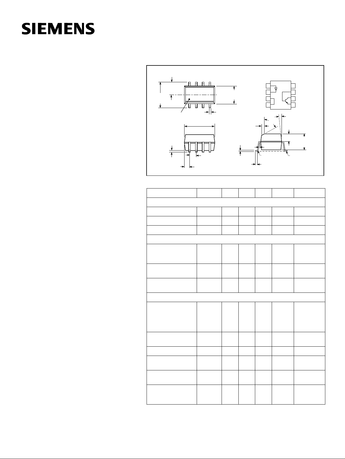
Dimensions in inches (mm)
• High Current Transfer Ratio, IF=1 mA
IL215A—20% Minimum
IL216A—50% Minimum
IL217A—100% Minimum
• Isolation V oltage, 2500 VA C
RMS
• Electrical Specifications Similar to
Standard 6 Pin Coupler
• Industry Standard SOIC-8 Surface
Mountable Package
• Standard Lead Spacing, .05"
• Available in Tape and Reel Option
(Conforms to EIA Standard RS481A)
• Compatible with Dual Wave, Vapor Phase
and IR Reflow Soldering
• Underwriters Lab File #E52744
(Code Letter P)
DESCRIPTION
The IL215A/216A/217A are optically coupled pairs
with a Gallium Arsenide infrared LED and a silicon
NPN phototransistor. Signal information, including
a DC level, can be transmitted by the device while
maintaining a high degree of electrical isolation
between input and output. The IL215A//216A/217A
comes in a standard SOIC-8 small outline package
for surface mounting which makes it ideally suited
for high density applications with limited space. In
addition to eliminating through-holes requirements,
this package conforms to standards for surface
mounted devices.
The high CTR at low input current is designed for
low power consumption requirements such as
CMOS microprocessor interfaces.
Maximum Ratings
Emitter
Peak Reverse Voltage.....................................6.0 V
Continuous Forward Current........................ 60 mA
Power Dissipation at 25
Derate Linearly from 25
°
C............................90 mW
°
C......................1.2 mW/°C
Detector
Collector-Emitter Breakdown Voltage...............30 V
Emitter-Collector Breakdown Voltage.................7 V
Collector-Base Breakdown Voltage..................70 V
Power Dissipation ......................................150 mW
Derate Linearly from 25
°
C......................2.0 mW/°C
Package
Total Package Dissipation at 25°C Ambient
(LED + Detector).....................................280 mW
Derate Linearly from 25
Storage Temperature .................. –55
Operating Temperature .............. –55
Soldering Time at 260
°
C......................3.3 mW/°C
°
C to +150°C
°
C to +100°C
°
C .............................10 sec.
.120±.005
(3.05±.13)
.240
6.10)
Pin One ID
.192±.005
(4.88±.13)
.004 (.10)
.008 (.20)
.021 (.53)
Characteristics
Emitter
Forward Voltage V
Reverse Current I
Capacitance C
Detector
Breakdown Voltage
Collector-Emitter
Emitter-Collector
Dark Current,
Collector-Emitter
Capacitance,
Collector-Emitter
Package
DC Current Transfer
Ratio
IL215A
IL216A
IL217A
Saturation Voltage,
Collector-Emitter
Isolation Test Voltage V
Capacitance,
Input to Output
Resistance,
Input to Output R
Switching Time ton,t
(T
A
=25°C)
.154±.005
C
L
(3.91±.13)
.016 (.41)
.015±.002
.008 (.20)
.050 (1.27)
typ.
Symbol Min. Typ. Max. Unit Condition
F
R
O
B
VCEO
B
VECO
I
CEOdark
C
CE
CTR
DC
V
CEsat
IO
C
IO
IO
off
.020±.004
(.15±.10)
20
50
100
2500 VAC
Anode
1
Cathode
(.38±.05)
2 plcs.
1.0 1.5 V IF=1 mA
0.1 100
25 pF VR=0
30
7
550nA VCE=10 V
10 pF VCE=0
50
80
130
0.5 pF
100 G
3.0
2
NC
3
NC
4
40°
5° max.
R.010
(.25) max.
0.5 IF=1 mA,
8
NC
7
Base
6
Collector
5
Emitter
7°
.058±.005
(1.49±.13)
.125±.005
(3.18±.13)
Lead
Coplanarity
±.0015 (.04)
max.
µ
AV
V
V
%I
Ω
µ
sI
IC=10 µA
IE=10 µA
IF=0
VCE=5 V
IC=0.1 mA
RMS
RE=100 Ω,
VCE=10 V
=6.0 V
R
=10 mA,
F
=2 mA,
C
5–1
This document was created with FrameMaker 4.0.4
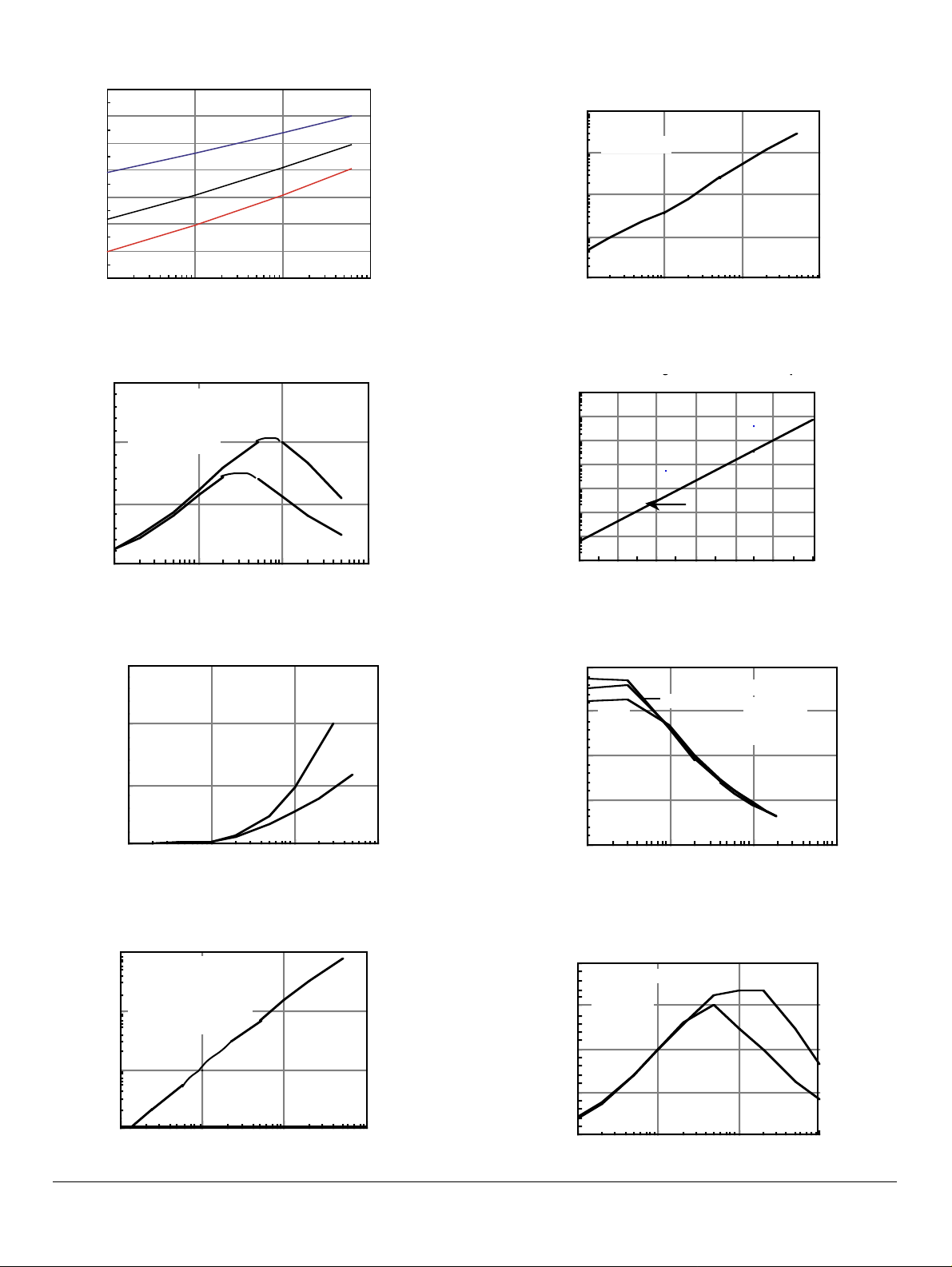
Figure 1. Forward voltage versus forward current
V
C
Collector emitter leakage current versus temperature
C
C
C
V
V
V
1.4
1.3
1.2
1.1
1.0
0.9
Vf-Forward Voltage - V
0.8
0.7
.1 1 10 100
Ta = -55°C
Ta = 25°C
Ta = 100°C
If- Forward Current - mA
Figure 5. Collector-base photocurrent versus
LED current
1000
Ta = 2 5°C
Vcb = 9.3 V
100
10
1
.1
.1 1 10 100
Icb - Collector-base Curr ent - µA
IF - LED Current - mA
Figure 2. Normalized non-saturated and saturated
CTRce versus LED current
1.5
Normalized to:
Vce = 10 V
I F = 10 mA
1.0
Ta = 25°C
V c e = 5 V
0.5
NCTRc e - Normalized CTRce
0.0
.1110100
Vce = 0.4 V
IF - L ED C u r re n t - mA
Figure 3. Collector-emitter current versus LED current
150
Ta = 25°
Vce = 10
100
50
Current - mA
Ice - Collector-emitter
0
.1 1 10 100
IF - LED Current - mA
Vce = 0.4 V
Figure 6. Collector-emitter leakage current versus
temperature
5
10
4
10
3
10
2
10
1
10
0
10
-1
10
Iceo - Collector-Emitter - nA
-2
10
Ta - Ambient Temperature - °C
Vce = 10V
TYPICAL
100806040200-20
Figure 7. Normalized saturated HFE versus base
current and temperature
2.0
1.5
1.0
0.5
Saturated HFE
NHFE(sat) - Normalized
0.0
1 10 100 1000
70°
25°
Vce = 0.4 V
50°
Ib - Base Current - µA
Normalized to:
Ib = 20µA
Vce = 10
Ta = 25 °C
Figure 4. Normalized collector-base photocurrent
versus LED current
100
Normalized to:
Vcb = 9.3 V
IF = 1 mA
10
Ta = 25 °C
1
NIcb - Normalized Icb
.1
.1110100
IF - LED Curr ent - mA
5–2
Figure 8. Normalized non-saturated and saturated
CTRce versus LED current
2.0
Normalized to:
Ta = 25 °C
1.5
Vce = 5 V
IF = 1 mA
1.0
0.5
0.0
NCTRce - Normalized CTRce
.1 1 10 100
IF - LED Current - mA
Vce = 5
Vce = .4
IL215A/216A/217A
 Loading...