

Siemens HYS64V4120GU-10, HYS72V4120GU-10 Datasheet
3.3V 4M x 64-Bit 2 BANK SDRAM Module
3.3V 4M x 72-Bit 2 BANK SDRAM Module
HYS64V4120GU-10
HYS72V4120GU-10
168 pin unbuffered DIMM Modules
• 168 Pin JEDEC Standard, Unbuffered 8 Byte Dual-In-Line SDRAM Module
for PC main memory applications
• 2 bank 4M x 64, 4M x 72 organisation
• Optimized for byte-write non-parity or ECC applications
• Fully PC66 layout compatible
• JEDEC standard Synchronous DRAMs (SDRAM)
• Performance:
-10
f
CK
t
AC
Max. Clock frequency 66 MHz @ CL=2
100 MHz @ CL=3
Max. access time from clock 9 ns @ CL=2
8 ns @ CL=3
• Single +3.3V(± 0.3V ) power supply
• Programmable CAS Latency, Burst Length and Wrap Sequence
(Sequential & Interleave)
• Auto Refresh (CBR) and Self Refresh
• Decoupling capacitors mounted on substrate
• All inputs, outputs are LVTTL compatible
• Serial Presence Detect with E
• Utilizes 16 / 18 2M x 8 SDRAMs in TSOPII-44 packages
• 4096 refresh cycles every 64 ms
• Gold contact pad
• Card Size: 133,35 mm x 29.21 mm x 4,00 mm for HYS64(72)V4120GU
2
PROM
Semiconductor Group 1
1 2.98
HYS64(72)V4120GU-10
4M x 64/72 SDRAM-Module
The HYS64(72)V4120GU-10 are industry standard 168-pin 8-byte Dual in-line Memory Modules
(DIMMs) which are organised as 4M x 64 and 4M x 72 in two banks high speed memory arrays
designed with Synchronous DRAMs (SDRAMs) for non-parity and ECC applications. The DIMMs
use 16 2M x 8 SDRAMs for the 4M x 64 organisation and additional two SDRAMs for the 4M x 72
organisation. Decoupling capacitors are mounted on the PC board.
2
The DIMMs have a serial presence detect, implemented with a serial E
protocol. The first 128 bytes are utilized by the DIMM manufacturer and the second 128 bytes are
available to the end user.
All SIEMENS 168-pin DIMMs provide a high performance, flexible 8-byte interface in a 133,35 mm
long footprint. This SDRAM module is available with a board-height of 1,15“.
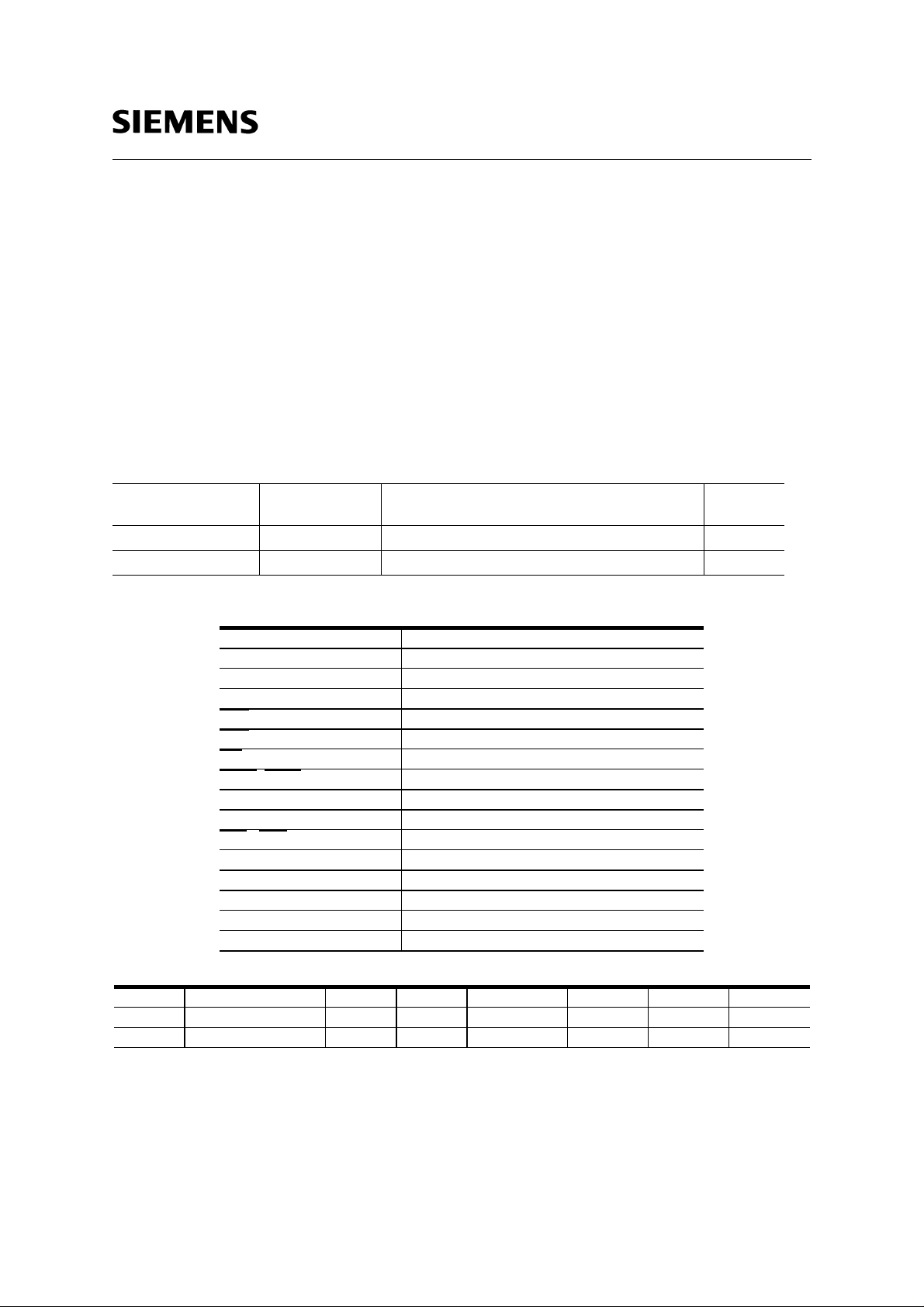
Ordering Information
Type Package Descriptions Module
HYS 64V4120GU-10 L-DIM-168-25 PC66 4M x 64 2 bank SDRAM module 1,15“
HYS 72V4120GU-10 L-DIM-168-25 PC66 4M x 72 2 bank SDRAM module 1,15“
PROM using the two pin I2C
Height
Pin Names
A0-A10 Address Inputs( RA0 ~ RA10 / CA0 ~ CA8)
BS (A11) Bank Select
DQ0 - DQ63 Data Input/Output
CB0-CB7 Check Bits (x72 organisation only)
RAS
CAS
WE
, CKE1 Clock Enable
CKE0
CLK0 - CLK3 Clock Input
DQMB0 - DQMB7 Data Mask
- CS3 Chip Select
CS0
Vcc Power (+3.3 Volt)
Vss Ground
SCL Clock for Presence Detect
SDA Serial Data Out for Presence Detect
N.C. No Connection
Row Address Strobe
Column Address Strobe
Read / Write Input
Address Format:
Part Number Rows Columns Bank Select Refresh Period Interval
4M x 64 HYS 64V4120GU 11 9 1 4k 64 ms 15,6 µs
4M x 72 HYS 72V4120GU 11 9 1 4k 64 ms 15,6 µs
Semiconductor Group 2
HYS64(72)V4120GU-10
4M x 64/72 SDRAM-Module
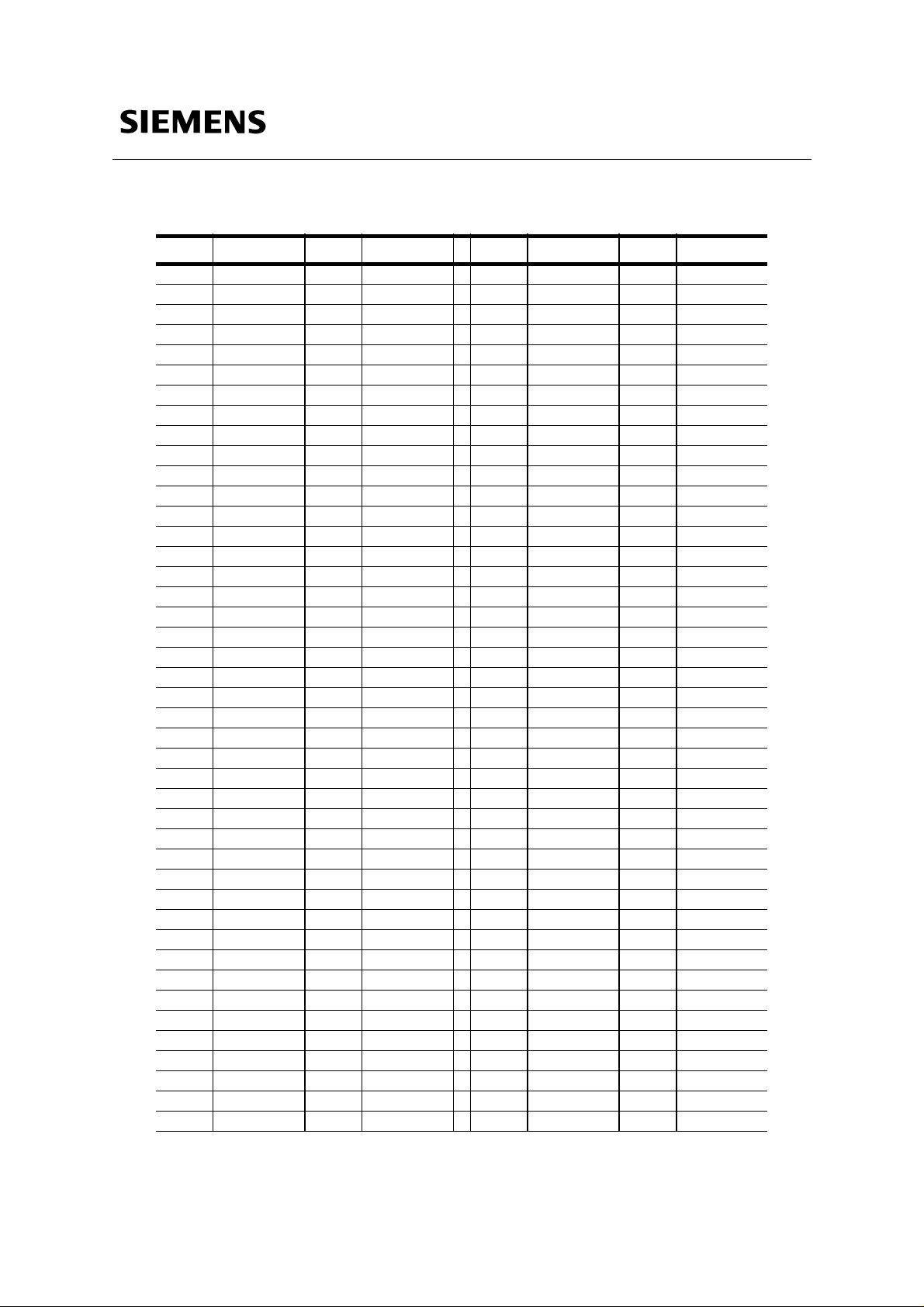
Pin Configuration
PIN # Symbol PIN # Symbol PIN # Symbol PIN # Symbol
1 VSS 43 VSS 85 VSS 127 VSS
2 DQ0 44 DU 86 DQ32 128 CKE0
3 DQ1 45 CS2 87 DQ33 129 CS3
4 DQ2 46 DQMB2 88 DQ34 130 DQMB6
5 DQ3 47 DQMB3 89 DQ35 131 DQMB7
6 VCC 48 DU 90 VCC 132 NC
7 DQ4 49 VCC 91 DQ36 133 VCC
8 DQ5 50 NC 92 DQ37 134 NC
9 DQ6 51 NC 93 DQ38 135 NC
10 DQ7 52 NC (CB2) 94 DQ39 136 CB6
11 DQ8 53 NC (CB3) 95 DQ40 137 CB7
12 VSS 54 VSS 96 VSS 138 VSS
13 DQ9 55 DQ16 97 DQ41 139 DQ48
14 DQ10 56 DQ17 98 DQ42 140 DQ49
15 DQ11 57 DQ18 99 DQ43 141 DQ50
16 DQ12 58 DQ19 100 DQ44 142 DQ51
17 DQ13 59 VCC 101 DQ45 143 VCC
18 VCC 60 DQ20 102 VCC 144 DQ52
19 DQ14 61 NC 103 DQ46 145 NC
20 DQ15 62 DU 104 DQ47 146 DU
21 NC (CB0) 63 CKE1 105 NC (CB4) 147 NC
22 NC (CB1) 64 VSS 106 NC (CB5) 148 VSS
23 VSS 65 DQ21 107 VSS 149 DQ53
24 NC 66 DQ22 108 NC 150 DQ54
25 NC 67 DQ23 109 NC 151 DQ55
26 VCC 68 VSS 110 VCC 152 VSS
27 WE 69 DQ24 111 CAS 153 DQ56
28 DQMB0 70 DQ25 112 DQMB4 154 DQ57
29 DQMB1 71 DQ26 113 DQMB5 155 DQ58
30 CS0 72 DQ27 114 CS1 156 DQ59
31 DU 73 VCC 115 RAS 157 VCC
32 VSS 74 DQ28 116 VSS 158 DQ60
33 A0 75 DQ29 117 A1 159 DQ61
34 A2 76 DQ30 118 A3 160 DQ62
35 A4 77 DQ31 119 A5 161 DQ63
36 A6 78 VSS 120 A7 162 VSS
37 A8 79 CLK2 121 A9 163 CLK3
38 A10 80 NC 122 A11=BS 164 NC
39 NC 81 NC 123 NC 165 SA0
40 VCC 82 SDA 124 VCC 166 SA1
41 VCC 83 SCL 125 CLK1 167 SA2
42 CLK0 84 VCC 126 NC 168 VCC
Note : Pinnames in brackets are for the x72 ECC versions
Semiconductor Group 3
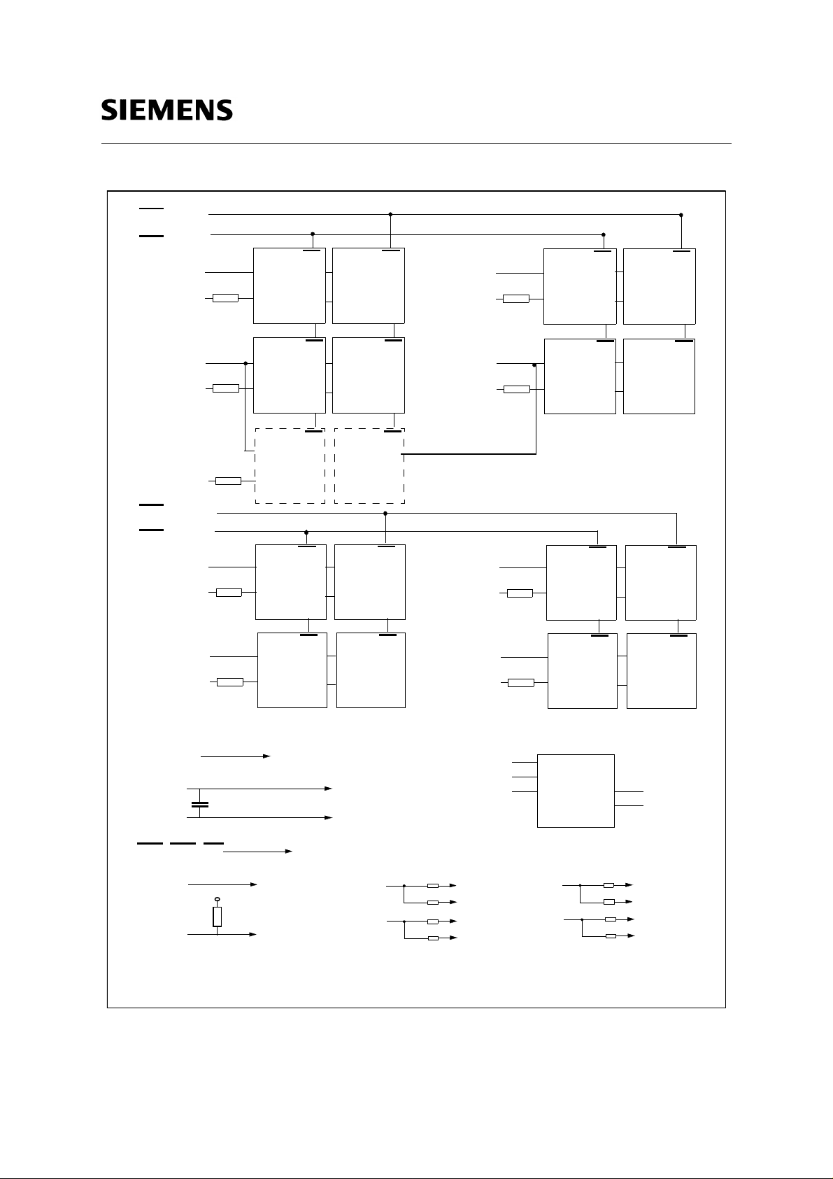
CS1
CS0
DQMB0
DQM
CS
DQM
CS
DQMB4
HYS64(72)V4120GU-10
4M x 64/72 SDRAM-Module
DQM
CS
DQM
CS
DQ0-DQ7
DQMB1
DQ8-DQ15
CB0-CB7
CS3
CS2
DQMB2
DQ16-DQ23
DQMB3
DQ24-DQ31
DQ0-DQ7
DQM
DQ0-DQ7
DQM
DQ0-DQ7
D16
CS
DQM
DQ0-DQ7
CS
DQM
DQ0-DQ7
D0
CS
D1
CS
D2
D3
DQ0-DQ7
DQM
DQ0-DQ7
DQM
DQ0-DQ7
D17
CS
DQM
DQ0-DQ7
D10
CS
DQM
DQ0-DQ7
D11
D8
CS
D9
CS
DQ32-DQ39
DQMB5
DQ40-DQ47
DQMB6
DQ48-DQ55
DQMB7
DQ56-DQ63
DQ0-DQ7
DQM
DQ0-DQ7
DQM
DQ0-DQ7
DQM
DQ0-DQ7
E2PROM (256wordx8bit)
DQ0-DQ7
D4
CS
DQM
DQ0-DQ7
D5
CS
DQM
DQ0-DQ7
D6
CS
DQM
DQ0-DQ7
D7
D12
CS
D13
CS
D14
CS
D15
A0-A10,BS
VDD
VSS
, CAS, WE
RAS
CKE0
CKE1
Note: D16 & D17 is only used in the x72 ECC version and all resistor values are 10 Ohms except otherwise noted.
C1-C15,(C16,C17)
VDD
10k
D0 - D15,(D16,D17)
D0 - D15,(D16,D17)
D0 - D7,(D8)
D0 - D15,(D16,D17)
D0 - D7,(D16)
D9 - D15,(D17)
CLK0
CLK2
SA0
SA1
SA2
2 SDRAMs
2 SDRAMs
2 SDRAMs
2 SDRAMs
SA0
SA1
SA2
CLK1
CLK3
SCL
SDA
Block Diagram for 4M x 64/72 SDRAM DIMM modules (HYS64/72V4120GU)
Semiconductor Group 4
2 (3) SDRAMs
2 SDRAMs
2 (3) SDRAMs
2 SDRAMs
 Loading...