

Siemens HYM72V8030GS-50, HYM72V8030GS-60, HYM72V8020GS-50, HYM72V8020GS-60 Datasheet
8M × 72-Bit Dynamic RAM Module
(ECC - Module)
HYM 72V8020GS-50/-60
HYM 72V8030GS-50/-60
168 pin buffered DIMM Module
• 168 pin JEDEC Standard, Buffered 8 Byte Dual In-Line Memory Module
for PC main memory applications
• 1 bank 8 M x 72 organisation
• Optimized for ECC applications
• Fast Page Mode Operation
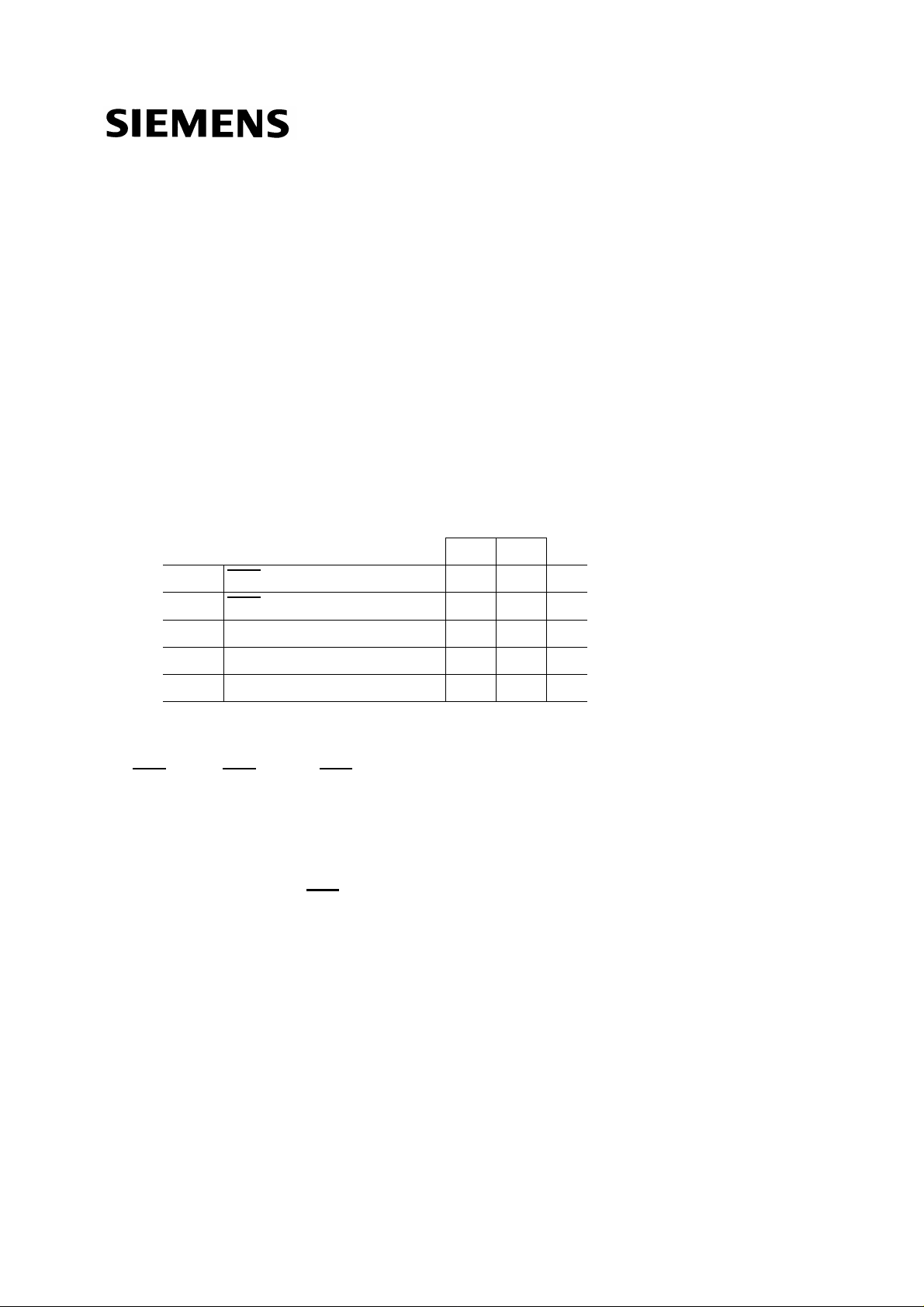
• Performance:
-50 -60
t
RAC
t
CAC
t
AA
t
RC
t
PC
RAS access time 50 60 ns
CAS access time 18 20 ns
Access time from address 30 35 ns
Read/Write cycle time 90 110 ns
Fast page mode cycle time 35 40 ns
• Single + 3.3V ± 0.3 V supply
• CAS-before-RAS refresh, RAS-only refresh
• Decoupling capacitors mounted on substrate
• All inputs, outputs and clock fully LVTTL & LVCMOS compatible
• 4 Byte interleave enabled, Dual Address inputs (A0/B0)
• Buffered inputs excepts RAS and DQ
• Parallel Presence Detects
• Utilizes nine 8M × 8 -DRAMs and BiCMOS buffers/line drivers VT244A
• Two versions: HYM 72V8030GS with SOJ-components ( 9 mm module thickness)
HYM 72V8020GS with TSOPII-components ( 4 mm module thickness)
• 4048 refresh cycles / 64 ms with 12 / 11 addressing
• Gold contact pad
• Double sided module with 25.35 mm (1000 mil) height
Semiconductor Group 1
1 6.96
HYM72V8020/30GS-50/-60
8M x 72-ECC Module
The HYM 72V8020/30GS-50/-60 is a 64 MByte DRAM module organized as 8 388 608 words by 72bit in a 168-pin, dual read-out, single-in-line package comprising nine HYB3165800AJ/AT 8M × 8
DRAMs in 400 mil wide SOJ or TSOPII - packages mounted together with ceramic decoupling
capacitors on a PC board. All inputs except RAS
line drivers.
Each HYB3165800AJ/AT is described in the data sheet and is fully electrically tested and
processed according to Siemens standard quality procedure prior to module assembly. After
assembly onto the board, a further set of electrical tests is performed.
The density and speed of the module can be detected by the use of presence detect pins.
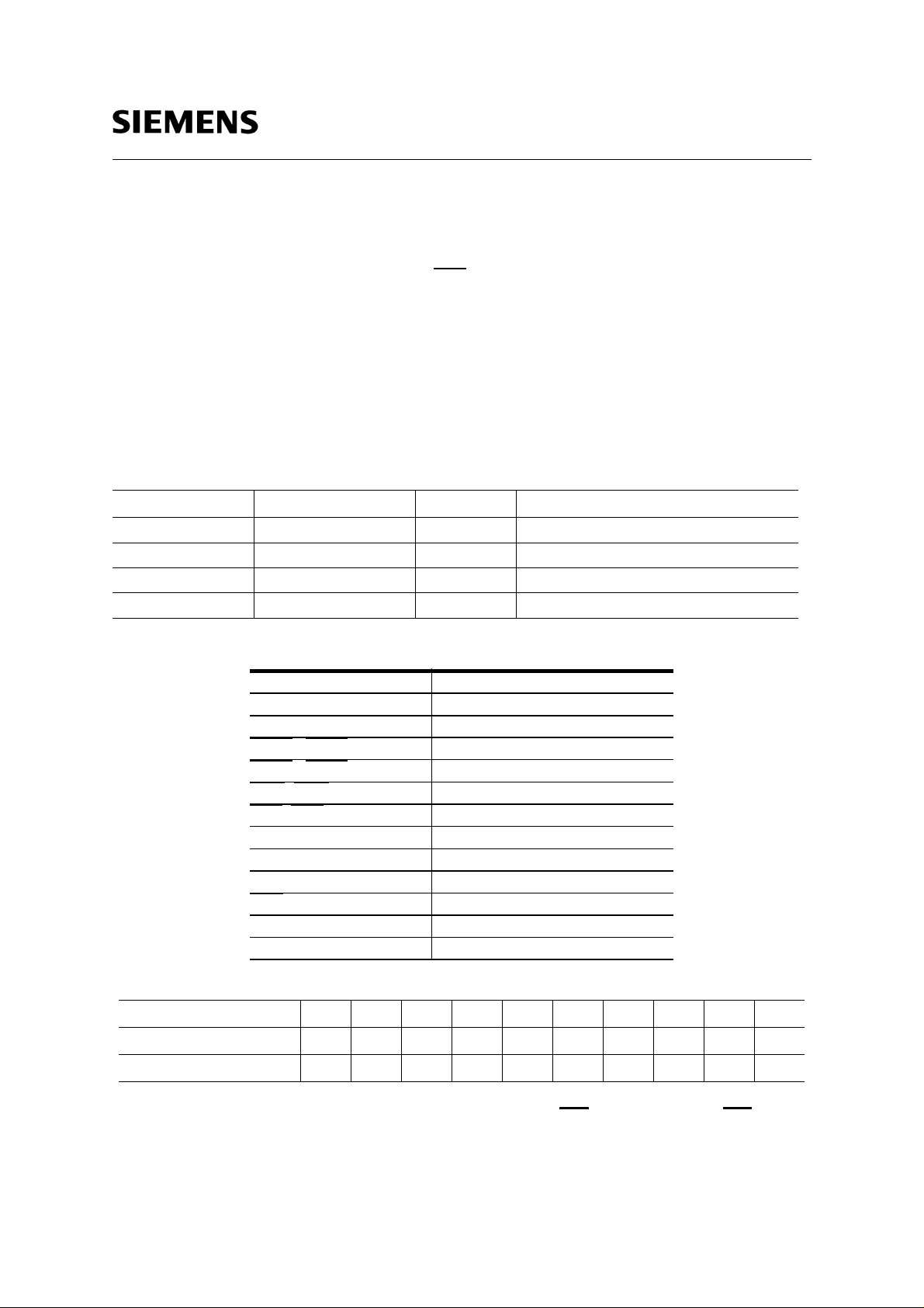
Ordering Information
Type Ordering Code Package Descriptions
HYM 72V8020GS-50 L-DIM-168-3 DRAM module (access time 50 ns)
HYM 72V8020GS-60 L-DIM-168-3 DRAM module (access time 60 ns)
HYM 72V8030GS-50 L-DIM-168-3 DRAM module (access time 50 ns)
HYM 72V8030GS-60 L-DIM-168-3 DRAM module (access time 60 ns)
and DQ are buffered by using BiCMOS buffers/
Pin Names
A0-A12,B0 Row Address Inputs
A0-A11,B0 Column Address Inputs
DQ0 - DQ71 Data Input/Output
, RAS2 Row Address Strobe
RAS0
, CAS2 Column Address Strobe
CAS0
, WE2 Read / Write Input
WE0
, OE2 Output Enable
OE0
Vcc Power (+3.3 Volt)
Vss Ground
PD1 - PD8 Presence Detect Pins
PDE
Presence Detect Enable
ID0 , ID1 ID indentification bit
N.C. No Connection
Presence-Detect and ID-pin Truth Table:
Module ID0 ID1 PD1 PD2 PD3 PD4 PD5 PD6 PD7 PD8
HYM 728020/30GS-50 Vss Vss 1 0 1 1 0 0 0 0
HYM 728020/30GS-60 Vss Vss 1 0 1 1 0 1 1 0
Note: 1 = High Level ( Driver Output) , 0 = Low Level (Driver Output) for PDE active ( ground) . For PDE at a high
level all PD terminal are in tri-state.
Semiconductor Group 2
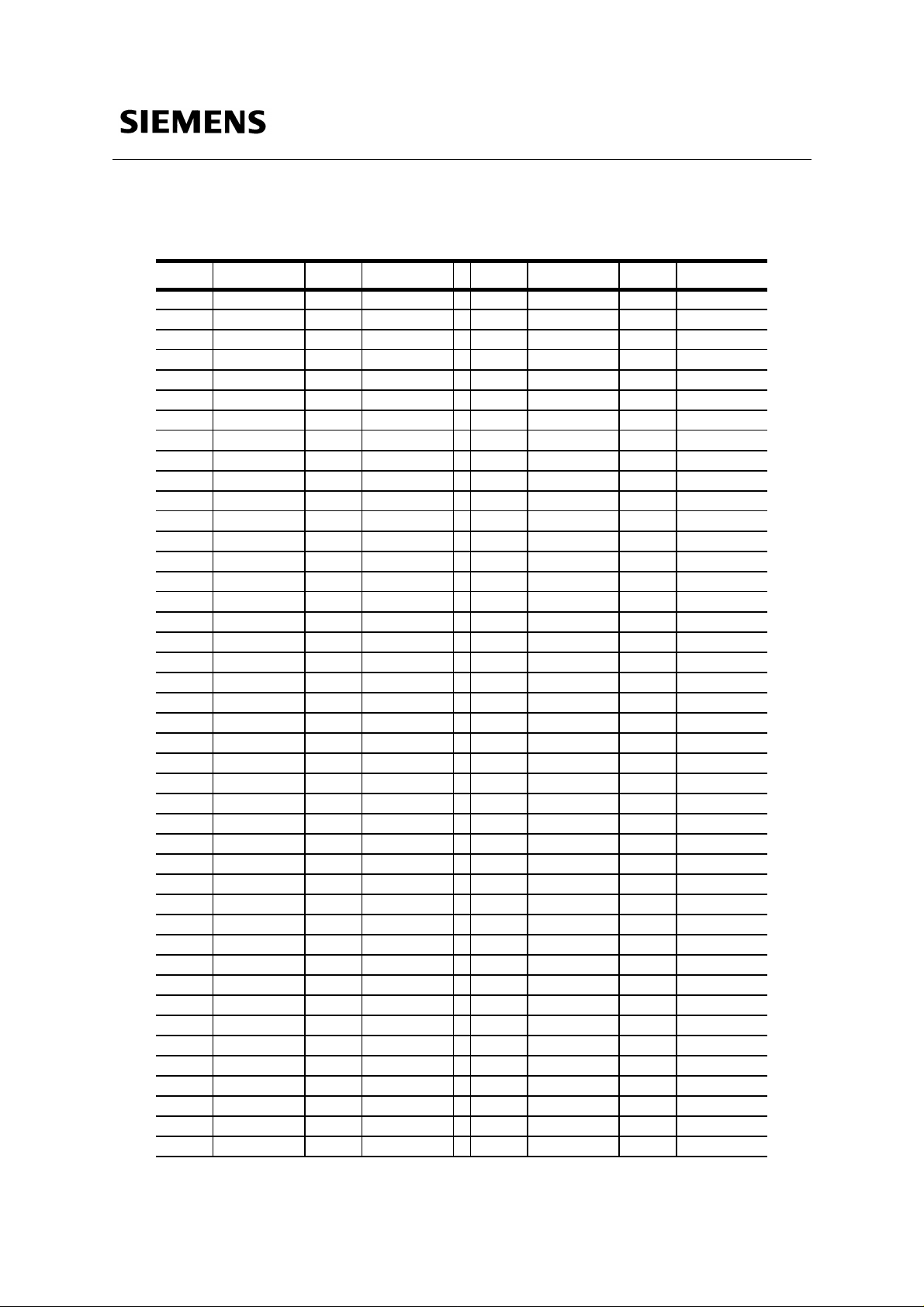
Pin Configuration
PIN # Symbol PIN # Symbol PIN # Symbol PIN # Symbol
1 VSS 43 VSS 85 VSS 127 VSS
2 DQ0 44 OE2 86 DQ36 128 NC
3 DQ1 45 RAS2 87 DQ37 129 NC
4 DQ2 46 CAS4 88 DQ38 130 NC
5 DQ3 47 NC 89 DQ39 131 NC
6 VCC 48 WE2 90 VCC 132 PDE
7 DQ4 49 VCC 91 DQ40 133 VCC
8 DQ5 50 NC 92 DQ41 134 NC
9 DQ6 51 NC 93 DQ42 135 NC
10 DQ7 52 DQ18 94 DQ43 136 DQ54
11 DQ8 53 DQ19 95 DQ44 137 DQ55
12 VSS 54 VSS 96 VSS 138 VSS
13 DQ9 55 DQ20 97 DQ45 139 DQ56
14 DQ10 56 DQ21 98 DQ46 140 DQ57
15 DQ11 57 DQ22 99 DQ47 141 DQ58
16 DQ12 58 DQ23 100 DQ48 142 DQ59
17 DQ13 59 VCC 101 DQ49 143 VCC
18 VCC 60 DQ24 102 VCC 144 DQ60
19 DQ14 61 NC 103 DQ50 145 NC
20 DQ15 62 NC 104 DQ51 146 NC
21 DQ16 63 NC 105 DQ52 147 NC
22 DQ17 64 NC 106 DQ53 148 NC
23 VSS 65 DQ25 107 VSS 149 DQ61
24 NC 66 DQ26 108 NC 150 DQ62
25 NC 67 DQ27 109 NC 151 DQ63
26 VCC 68 VSS 110 VCC 152 VSS
27 WE0 69 DQ28 111 NC 153 DQ64
28 CAS0 70 DQ29 112 NC 154 DQ65
29 NC 71 DQ30 113 NC 155 DQ66
30 RAS0 72 DQ31 114 NC 156 DQ67
31 OE0 73 VCC 115 NC 157 VCC
32 VSS 74 DQ32 116 VSS 158 DQ68
33 A0 75 DQ33 117 A1 159 DQ69
34 A2 76 DQ34 118 A3 160 DQ70
35 A4 77 DQ35 119 A5 161 DQ71
36 A6 78 VSS 120 A7 162 VSS
37 A8 79 PD1 121 A9 163 PD2
38 A10 80 PD3 122 A11 164 PD4
39 NC 81 PD5 123 NC 165 PD6
40 VCC 82 PD7 124 VCC 166 PD8
41 NC 83 ID0 (VSS) 125 NC 167 ID1 (VSS)
42 NC 84 VCC 126 B0 168 VCC
HYM72V8020/30GS-50/-60
8M x 72-ECC Module
Semiconductor Group 3
HYM72V8020/30GS-50/-60
8M x 72-ECC Module
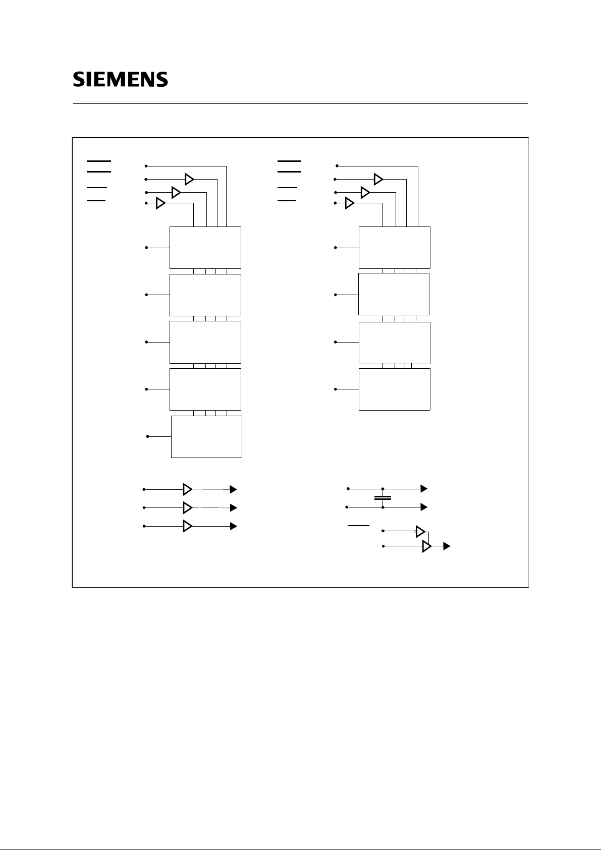
RAS0
CAS0
WE0
OE0
DQ0-DQ7
DQ8-DQ15
DQ16-DQ23
DQ24-DQ31
DQ32-DQ39
I/O1-I/O8
I/O1-I/O8
I/O1-I/O8
I/O1-I/O8
I/O1-I/O8
D0
D1
D2
D3
D4
RAS2
CAS4
WE2
OE2
DQ40-DQ47
DQ48-DQ55
DQ56-DQ63
DQ64-DQ71
I/O1-I/O8
D5
I/O1-I/O8
D6
I/O1-I/O8
D7
I/O1-I/O8
D8
A0
B0
A1-A11
Block Diagram
D0 - D4
D5 - D8
D0 - D8
Vcc
Vss
PDE
Vcc or Vss
D0-D8, buffers
PD1-PD8
Semiconductor Group 4
 Loading...