GaAs MMIC CGY 60
________________________________________________________________________________________________________
D a t a s h e e t
*Low noise preamplifier for mobile communication
(PCN, DECT, GSM) in 2.7V to 6V systems
*Biased monolithic microwave IC (MMIC)
Matched to 50Ω for 1.7 to 2GHz
*Easily matchable to 50Ω for lower frequencies
(i.e. GSM-application)
*No bias coil needed
*Low noise figure and high gain
(typ. NF=1.9dB, G=12.5dB @ 3V, 1.85GHz)
*Low power consumption
*Frequency range 200 MHz ... 2.5 GHz
ESD: Electrostatic discharge sensitive device,
observe handling precautions!
RF-GND
Vd
6
RF-out
5
4
1
DC-GND
2
RF-GND
3
RF-in
Type Marking Ordering code
(taped)
Package 1)
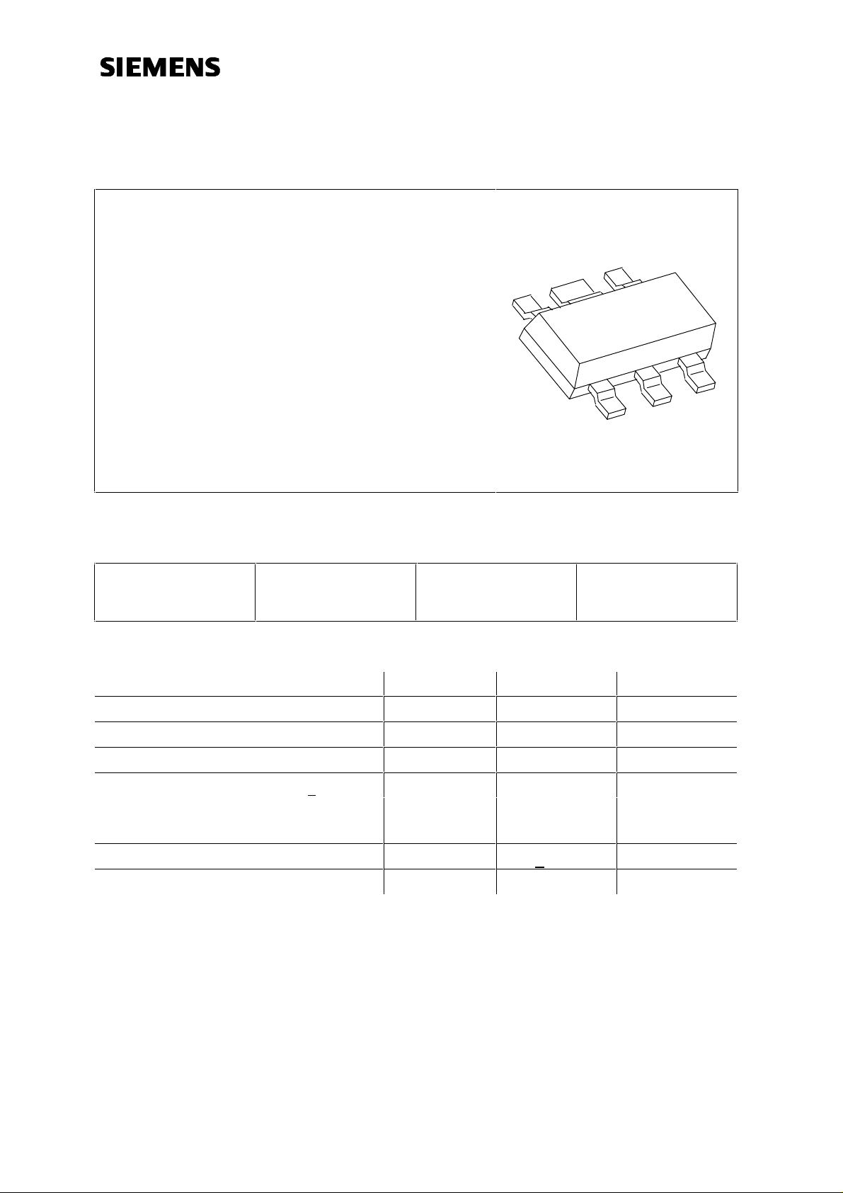
CGY 60 Y7s Q62702G-39 MW-6
Maximum ratings Symbol Unit
Drain voltage
Channel temperature
Storage temperature range
Total power dissipation (TS < 132°C)
Thermal resistance
Channel-soldering point (GND)
Channel-ambient
3)
2)
R
R
V
T
T
P
8V
150 °C
-55...+150 °C
80 mW
< 220 K/W
< 300 K/W
1) Dimensions see chapter Package Outlines
2) Please care for sufficient heat dissipation on the pcb!
3) Package mounted on alumina 15 mm x 16.7 mm x 0.7 mm
Siemens Aktiengesellschaft pg. 1/7 12.01.96
HL EH PD 21

GaAs MMIC CGY 60
________________________________________________________________________________________________________
Electrical characteristics of CGY60 in GSM application circuit
T
= 25°C f=950MHz RS = RL = 50 Ω
A
unless otherwise specified
Characteristics Symbol min typ max Unit
Drain current
Power Gain
Ud = 3V
Ud = 5V
Noise figure
Ud = 3V
Ud = 5V
Input return loss
Ud = 3V
Ud = 5V
Output return loss
Ud = 3V
Ud = 5V
Third order input intercept point
two-tone intermodulation test
f1 = 950MHz, f2 = 951MHz
Pin = -20dBm (both carriers)
Ud = 3V
Ud = 5V
RL
RL
IP
I
mA
-69
G
F
-
-
-
-
15.5
17
1.35
1.30
-
-
-
-
dB
dB
dB
-
-
10
10
-
dB
-
-
11
11
-
-
dBm
-
-
-3
-1
-
-
Input power at
P
-
dBm
1dB gain compression
Ud = 3V
Ud = 5V
Siemens Aktiengesellschaft pg. 2/7 12.01.96
-
-
-10
-8
-
-
HL EH PD 21

GaAs MMIC CGY 60
________________________________________________________________________________________________________
Electrical characteristics in PCN-, DECT-application circuit
T
= 25°C f=1850MHz RS = RL = 50 Ω
A
unless otherwise specified
Characteristics Symbol min typ max Unit
Drain current
Power Gain
Ud = 3V
Ud = 5V
Noise figure
Ud = 3V
Ud = 5V
Input return loss
Ud = 3V
Ud = 5V
Output return loss
Ud = 3V
Ud = 5V
Third order input intercept point
two-tone intermodulation test
f1 = 1850MHz, f2 = 1851MHz
Pin = -20dBm (both carriers)
Ud = 3V
Ud = 5V
RL
RL
IP
I
mA
-69
G
F
-
-
-
-
12.5
13.5
1.90
1.85
-
-
-
-
dB
dB
dB
-
-
14.5
14.5
-
dB
-
-
14
14
-
-
dBm
-
-
0
2
-
-
Input power at
P
-
dBm
1dB gain compression
Ud = 3V
Ud = 5V
Siemens Aktiengesellschaft pg. 3/7 12.01.96
-
-
-7
-5
-
-
HL EH PD 21
