Siemens CGY52 Datasheet

GaAs MMIC CGY 52
________________________________________________________________________________________________________
D a t a s h e e t
* Two stages monolithic microwave IC (MMIC Amplifier)
*All gold metallisation
*Chip fully passivated
*Operating voltage range: 2.7 to 5 V
*50 Ω input / output
ESD: Electrostatic discharge sensitive device,
observe handling precautions!
Type Marking Ordering code
(taped)
Package 1)
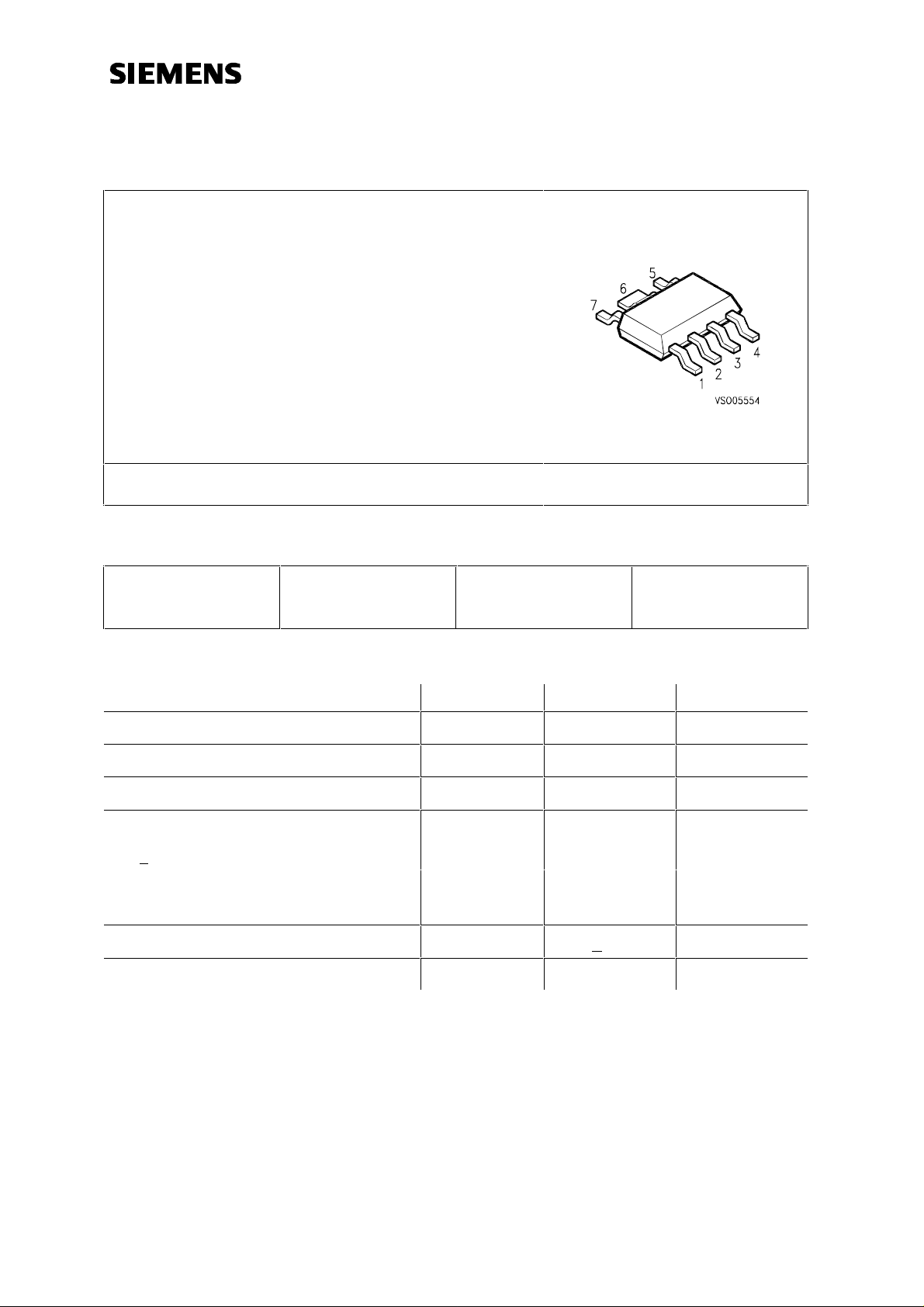
CGY 52 CGY52 Q68000-A8615 MW-7
Maximum ratings Symbol Unit
Drain voltage
Channel temperature
Storage temperature range
Total power dissipation
(TS < 55°C)
2) 3)
Thermal resistance
Channel-soldering point (GND)
Junction-ambient
4)
2)
V
T
T
P
R
thChS
R
thJA
D
Ch
stg
tot
6V
150 °C
-55...+150 °C
1000 mW
< 95 K/W
< 175 K/W
1) Dimensions see chapter Package Outlines
2) TS is measured on the source 2 lead at the soldering point of the pcb.
3) Please care for sufficient heat dissipation on the pcb!
4) Package mounted on alumina 15mm x16.7 mm x0.7 mm
Siemens Aktiengesellschaft pg. 1/4 12.02.96
HL EH PD 21

GaAs MMIC CGY 52
________________________________________________________________________________________________________
Electrical characteristics
T
= 25°C VD = 4.5 V RS = RL = 50Ω
A
unless otherwise specified
Characteristics Symbol min typ max Unit
Drain current
Power Gain
f = 200 MHz
f = 900 MHz
f = 1800 MHz
Gain flatness
f = 200 MHz to 1800 MHz
Noise figure
f = 900 MHz to 1800 MHz
Input return loss
f = 200 MHz to 300 MHz
f = 300 MHz to 1800 MHz
f = 200 MHz
f = 900 MHz
f = 1800 MHz
Output return loss
f = 200 MHz to 1800 MHz
f = 200 MHz
f = 900 MHz
f = 1800 MHz
∆
RL
RL
I
D
G
F
G
in
out
- 160 220 mA
13
14.5
12.5
14
15.5
13.5
-
dB
-
-
-34dB
- 4.8 - dB
6.5
7.5
-
-
-
9.5
-
-
-
7.5
8.5
7.5
12.5
9
10.5
10.5
12.5
11.5
-
dB
-
-
-
-
-
dB
-
-
-
Third order input intercept point
two-tone intermodulation test
f1 = 806 MHz, f2 = 810 MHz
= 10 dBm (both carriers)
P
=
1dB gain compression
f = 200 MHz to 1800 MHz
Siemens Aktiengesellschaft pg. 2/4 12.02.96
P
IP
-1
3
dB
- 32 - dBm
-19-
dBm
HL EH PD 21
 Loading...