Siemens CGY40 Datasheet

GaAs MMIC CGY 40
________________________________________________________________________________________________________
D a t a s h e e t
* Single-stage monolithic microwave IC ( MMIC amplifier )
* Application range: 100 MHz to 3 GHz
* Gain: 9 dB typ. @ 1.6 GHz
* Low noise figure: 2.7 dB typ. @ 1.6 GHz
* Bandwidth: 3 GHz typ. @ -3 dB, VSWR < 2 : 1
* Operating voltage range: 3 to 5.5 V
* Individual current control with neg. gate bias
* Hermetically sealed ceramic stripline package
Cerec-X
ESD: Electrostatic discharge sensitive device,
observe handling precautions!
Type Marking Ordering code
(tape and reel)
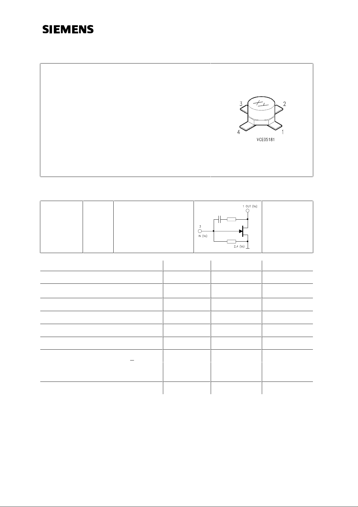
Circuit Diagram
(Pin Configuration)
Package 1)
CGY 40 40 Q68000-A4444 Cerec-X
Maximum ratings Symbol Value Unit
Drain-voltage
Current control gate voltage
Drain-gate voltage
Input power
Channel temperature
Storage temperature range
Total power dissipation (TS < 82°C)
2)
V
T
T
V
V
P
P
D
G
DG
IN
Ch
stg
tot
5.5 V
-3 ... 0 V
8.5 V
16 dBm
150 °C
-55...+150 °C
440 mW
Thermal resistance
Channel-soldering point
Note: Exceeding any of the max. ratings may cause permanent damage to the device. Appropriate handling is
required to protect the electrostatic sensitive MMIC against degradation due to excess voltage or current spikes.
Proper ground connection of leads 2 and 4 ( with min. inductance ) is required to achieve the guaranteed RF
performance, stable operating conditions and adequate cooling.
1) Dimensions see chapter Package Outlines
2) Ts is measured on the source lead at the soldering point to the PCB.
Siemens Aktiengesellschaft pg. 1/5 11.01.1996
2)
R
thChS
155 K/W
HL EH PD 21

GaAs MMIC CGY 40
________________________________________________________________________________________________________
Electrical Characteristics
TA = 25 °C, VG = 0 V, VD = 4.5 V, RS = RL = 50 Ω, unless otherwise specified
( for application circuit see next page )
Characteristics Symbol min typ max Unit
Drain current
Power gain
f = 200 MHz
f = 1800 MHz
Gain flatness
f = 200 to 1000 MHz
f = 800 to 1800 MHz
Noise figure
f = 200 to 1000 MHz
f = 800 to 1800 MHz
Input return loss
f = 200 to 1000 MHz
f = 800 to 1800 MHz
Output return loss
f = 200 to 1000 MHz
f = 800 to 1800 MHz
∆
RL
RL
I
G
F
G
-6080
9.5
8
-
-
-
-
-
-
-
-
10.5
9
0.4
1.1
2.5
2.8
13
12
12
12
12
10.5
-
2
-
4.0
-
9.5
-
9.5
mA
dB
dB
dB
dB
dB
Third order intercept point
Two tone intermodulation test
= 806 MHz, f
f
P
= 10 dBm ( both carriers )
0
= 810 MHz
1dB gain compression
f = 200 to 1800 MHz
Gain control dynamic range
f = 200 to 1000 MHz
f = 800 to 1800 MHz
Siemens Aktiengesellschaft pg. 2/5 11.01.1996
IP3
P
∆
G
31 32 -
-18-
-
-
30
20
-
-
HL EH PD 21
dBm
dBm
dB
 Loading...