

GaAs MMIC
Preliminary Data
l
Broadband Power Amplifier [ 800..3500 Mhz ]
l
DECT,PHS,PCS,GSM,AMPS,WLAN,WLL
l
Single Voltage Supply
l
Operating voltage range: 2.0to 6 V
l
Pout = 25.5dBm at Vd=2.4V
l
Pout = 27.0dBm at Vd=3.0V
l
Pout = 30.0dBm at Vd=5.0V
l
Overall power added efficiency up to 50 %
l
Easy external matching
ESD: Electrostatic discharge sensitive device,
observe handling precautions!
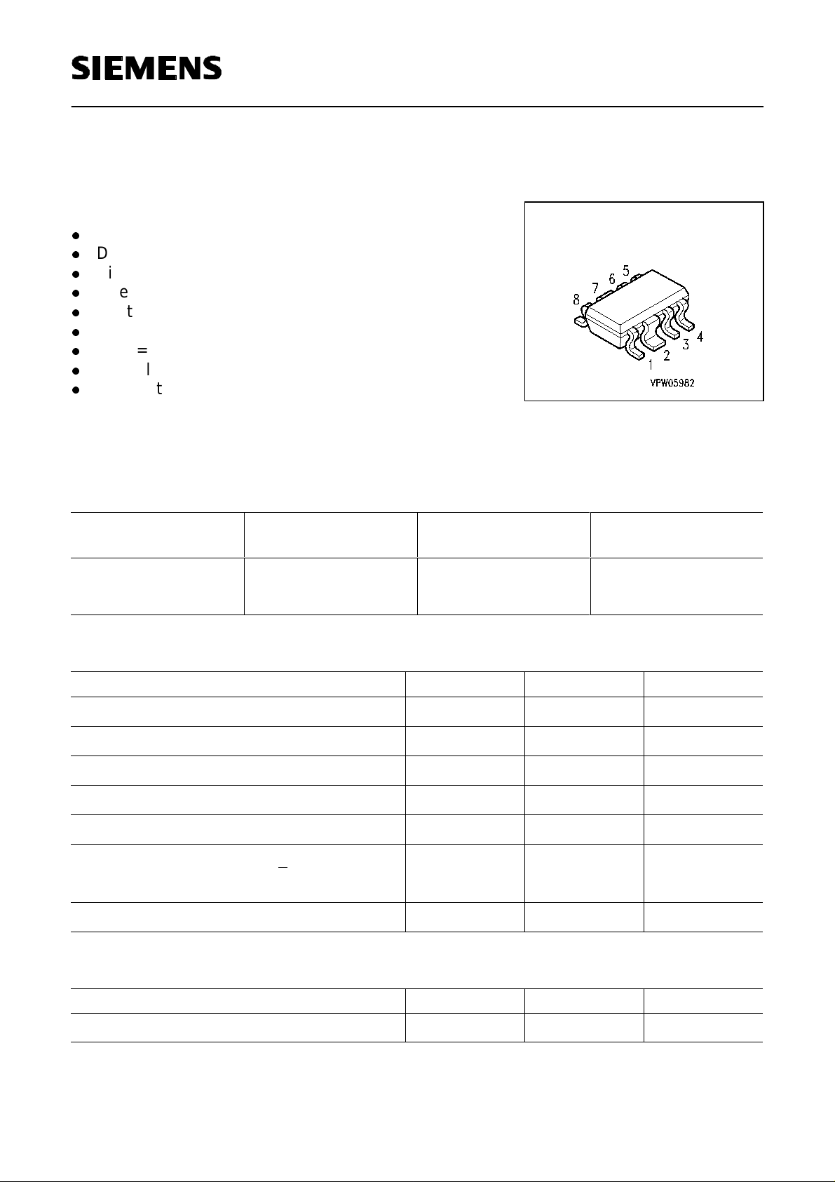
CGY 196
Type Marking Ordering code
Package
(taped)
CGY 196 t.b.d. t.b.d. SCT598
Maximum ratings
Characteristics Symbol max. Value Unit
Positive supply voltage V
Supply current
Maximum input power
Channel temperature
Storage temperature
Total power dissipation
(Ts < 81 °C)
Pinmax
T
T
P
Ts: Temperature at soldering point
Pulse peak power
P
Pulse
D
I
D
Ch
stg
tot
6V
1.0 A
20 dBm
150 °C
-55...+150 °C
1.0 W
2.0 W
Thermal Resistance
Characteristics Symbol max. Value Unit
Channel-soldering point
Siemens Aktiengesellschaft 1 16.6.1998
Semiconductor Group 1 1998-11-01
HL HF PE GaAs
R
thChS
70 K/W
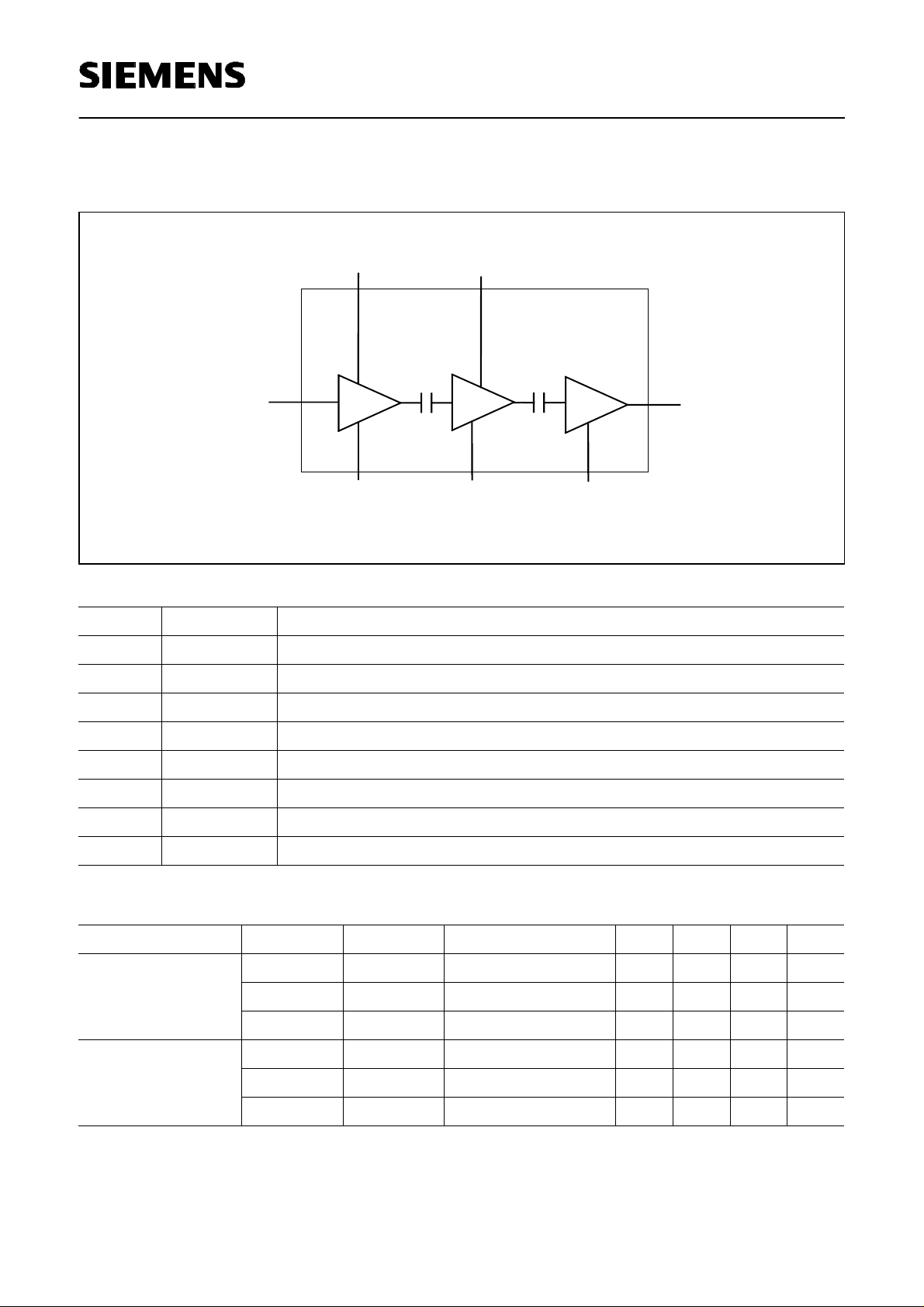
Functional Block Diagram
CGY 196
Pin #
Name
VD1
RFin/Vg
GND
Configuration
VD2
GND
GND
1 RFin/Vg RF input power + Gate voltage [0V internal]
2 GND RF and DC ground
3 VD2 Pos. drain voltage of the 2nd stage
RFout/Vd3
4 n.c. not connected
5 n.c. not connected
6 RFout/VD3 RF output power / Pos. drain voltage of the 3rd stage
7 GND RF and DC ground
8 VD1 Pos. drain voltage of the 1st stage
DC characteristics
Characteristics Symbol Conditions min typ max Unit
Drain current
Transconductance
stage 1
stage 2
stage 3
stage 1
stage 2
stage 3
IDSS1
IDSS2
IDSS2
gfs1
gfs2
gfs3
VD1=3V 45 mA
VD2=3V 65 mA
VD2=3V 340 mA
VD=3V, ID=50mA 110 mS
VD=3V, ID=300mA 650 mS
VD=3V, ID=300mA 650 mS
Siemens Aktiengesellschaft 2 16.6.1998
Semiconductor Group 2 1998-11-01
HL HF PE GaAs
CGY 196
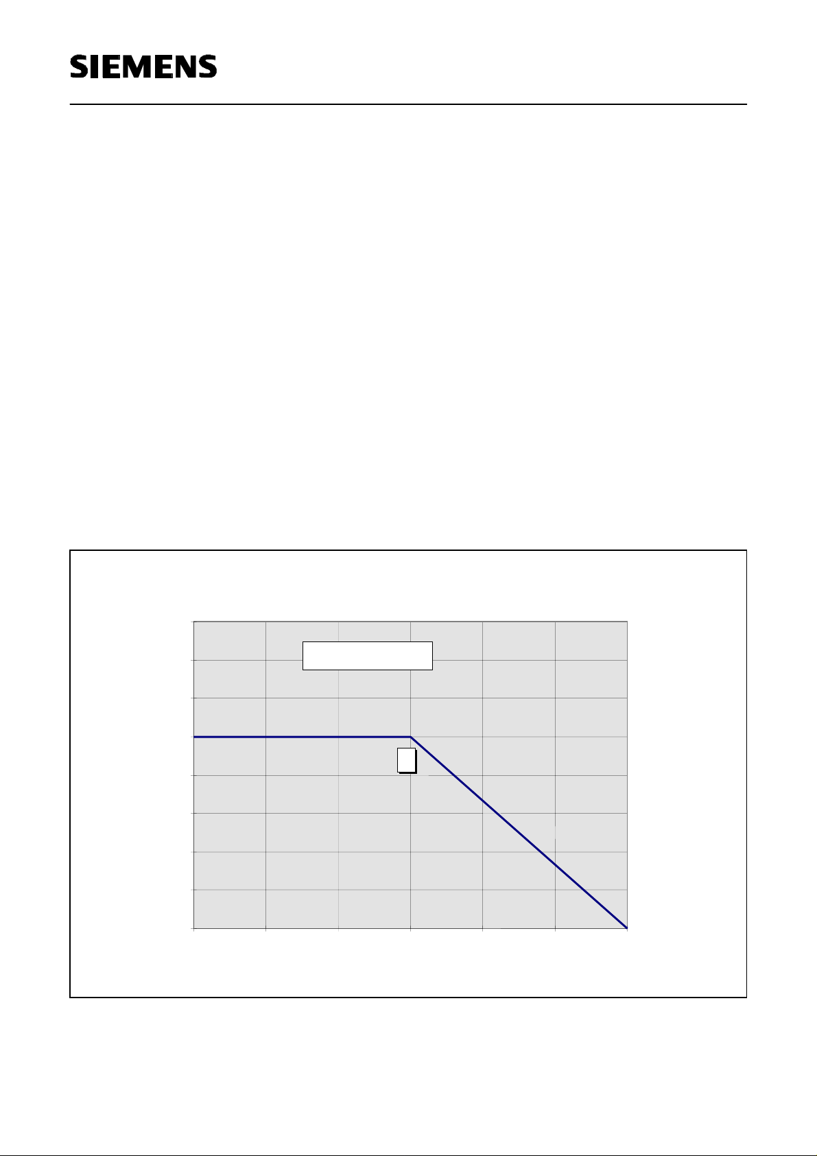
Determination of Permissible Total Power Dissipation for Continuous and Pulse
Operation
The dissipated power is the power which remains in the chip and heats the device. It does
not contain RF signals which are coupled out consistently.
a) Continuous Wave / DC Operation
For the determination of the permissible total power dissipation P
from the diagram
tot-DC
below it is necessary to obtain the temperature of the soldering point TS first. There are two
cases:
• When R
(soldering point to ambient) is not known: Measure TS with a temperature
thSA
sensor at the leads were the heat is transferred from the device to the board ( normally at
the widest source or ground lead for GaAs ). Use a small sensor of low heat transport,
for example a thermoelement ( < 1mm ) with thin wires or a temperature indicating paper
while the device is operating.
• When R
is already known: TS = P
thSA
mW
1600
1400
1200
Permissible Total Power Dissipation in DC Operation
P
tot DC
= f (Ts)
diss
x R
thSA
+ T
A
1000
75
800
600
400
200
0
0 25 50 75 100 125 150
Temperature of soldering point, Ts °C
Siemens Aktiengesellschaft 3 16.6.1998
Semiconductor Group 3 1998-11-01
HL HF PE GaAs
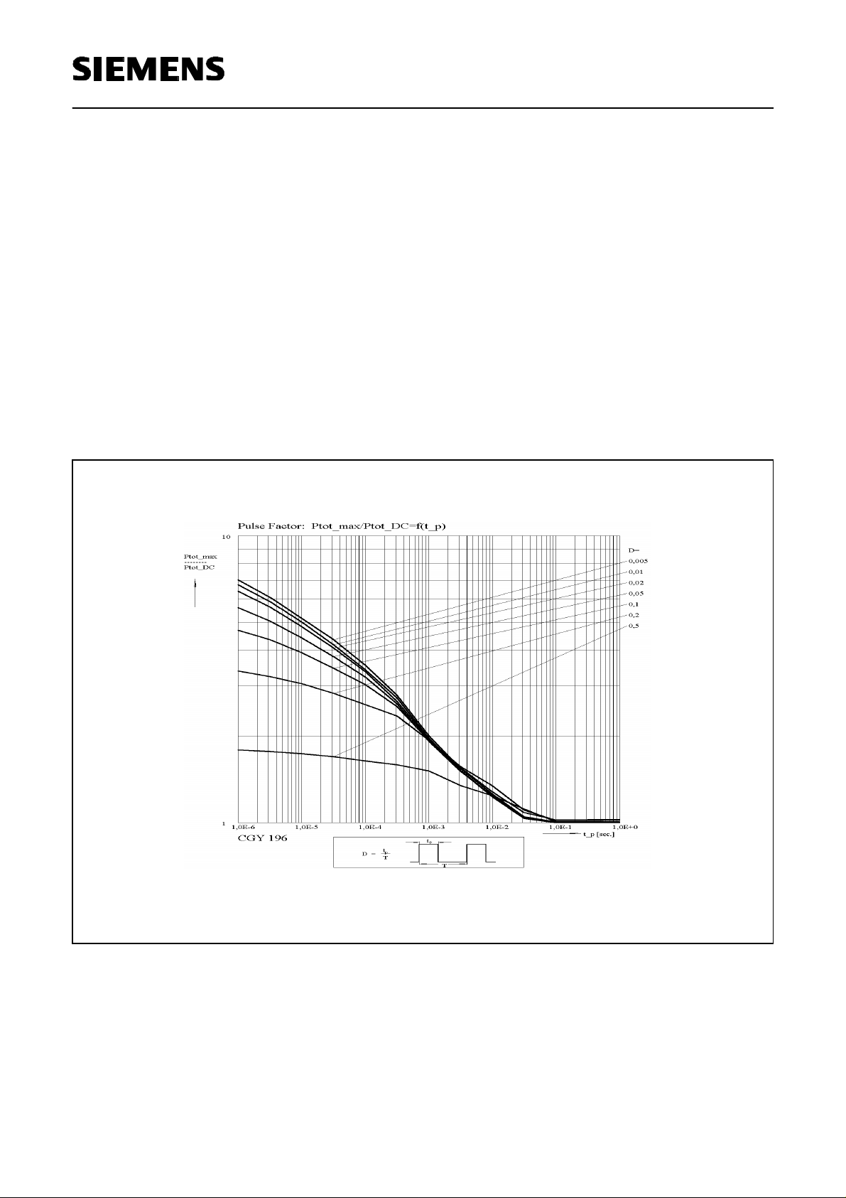
b) Pulsed Operation
For the calculation of the permissible pulse load P
P
tot-max
Use the values for P
from the following diagram to get a specific value.
as derived from the above diagram and for the
tot-DC
pulse factor = P
= P
= P
tot-DC
tot-DC
x ( P
tot-max
tot-max
Pulse factor:
the following formula is applicable:
tot-max
x Pulse factor
/ P
/ P
tot-DC
tot-DC
)
CGY 196
P
P
Siemens Aktiengesellschaft 4 16.6.1998
Semiconductor Group 4 1998-11-01
HL HF PE GaAs
should not exceed the absolute maximum rating for the dissipated power
tot-max
= ” Pulse peak power ” = 2 W
Pulse
CGY 196
c) Reliability Considerations
This procedure yields the upper limit for the power dissipation for continuous wave (cw) and
pulse applications which corresponds to the maximum allowed channel temperature. For
best reliability keep the channel temperature low. The following formula allows to track the
individual contributions which determine the channel temperature.
T
= ( P
ch
Channel temperature (=
junction temperature)
diss
Power dissipated in the chip. I t
does not contain decoupled RFpower
x R
) +
thChS
Rth of device from channel to
soldering point
T
S
Temperature of soldering point,
measured or calculated
Siemens Aktiengesellschaft 5 16.6.1998
Semiconductor Group 5 1998-11-01
HL HF PE GaAs
 Loading...