

GaAs MMIC
Preliminary Data
l
Power amplifier for PCN applications
l
2.5 W (34dBm) output power at 3.5 V
l
Overall power added efficiency 43 %
l
Fully integrated 4 stage amplifier
l
Power ramp control
l
Input matched to 50 ohms, simple output match
ESD: Electrostatic discharge sensitive device,
observe handling precautions!
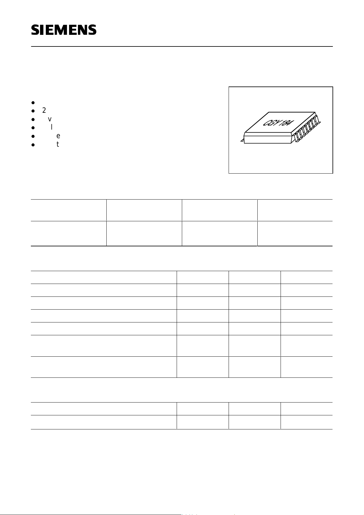
CGY 184
Type Marking Ordering code
Package
1)
(taped)
CGY 184 CGY 184 Q62702G62 MW 16
Maximum ratings
Characteristics Symbol max. Value Unit
Positive supply voltage V
Supply current
Channel temperature
Storage temperature
Pulse peak power dissipation
T
T
P
Pulse
duty cycle 12.5%, ton=0.577ms
Total power dissipation (Tc &
P
Tc: Temperature on case
D
I
D
Ch
stg
tot
9V
4A
150 °C
-55...+150 °C
tbd W
8.5 W
Thermal Resistance
Characteristics Symbol max. Value Unit
Junction-Case
1)
Dimensions see page 14
2)
see also page 9
Siemens Aktiengesellschaft 1 23.07.97
Semiconductor Group 1 1998-11-01
2)
R
thJC
≤8.5
K/W
HL HF PE GaAs
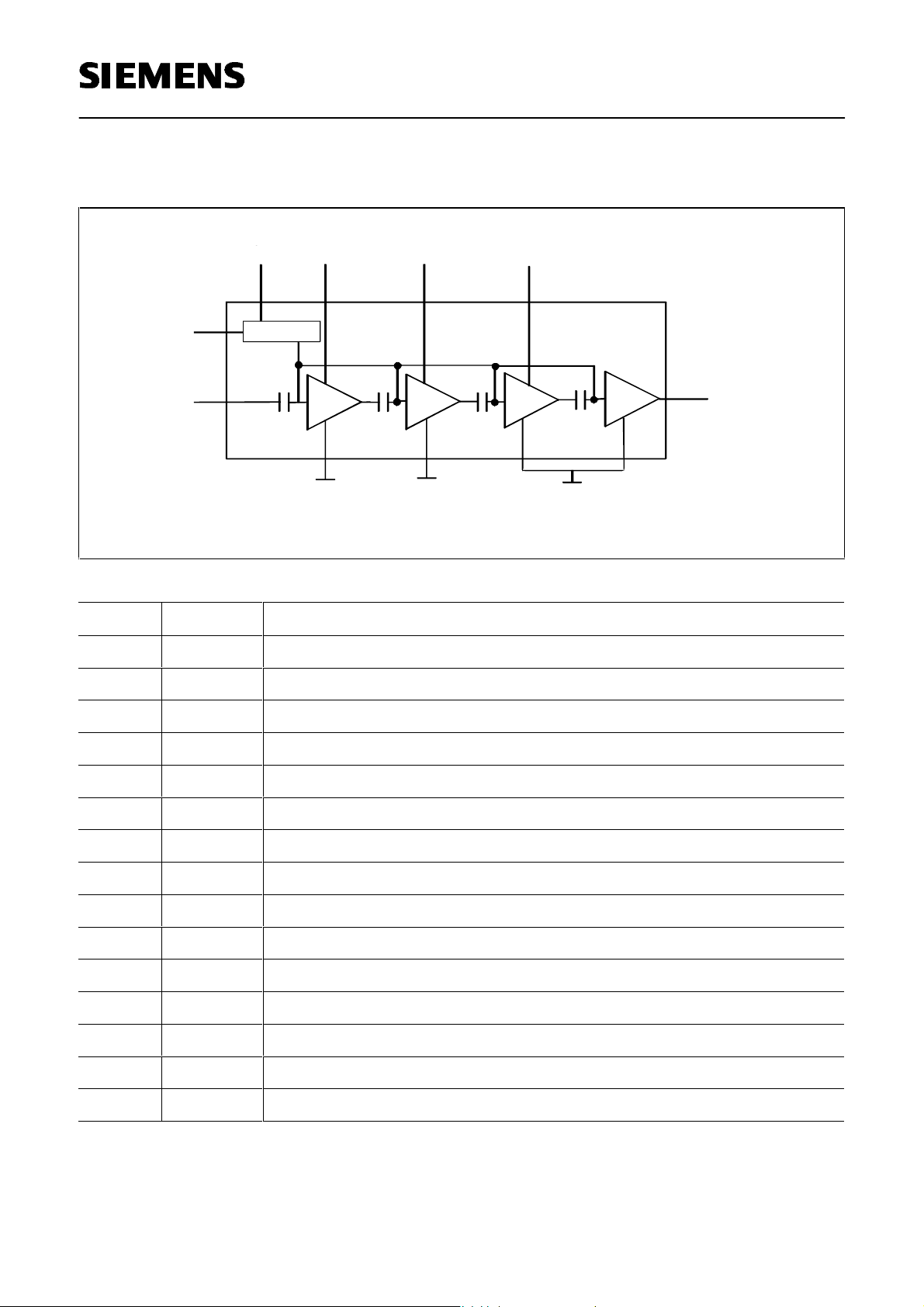
Functional block diagram
V
V
Vc
V
V
on
(2
)
D1(4)
D2(7)
CGY 184
D3(8)
neg(15)
Pin(3)
control circuit
GND1(5)
GND2(6)
Pin # Configuration
1n. c.
2 Vcon Control voltage for power ramping
3PINRF-input
4VD1Drain voltage 1st stage
Pout/VD4 (9,10,11
GND3(17)
5 Gnd1 Ground pin 1st stage
6 Gnd2 Ground pin 2nd stage
7VD2Drain voltage 2nd stage
8VD3Drain voltage 3rd stage
9,10,11 P
OUT/VD4
Drain voltage 4th stage and RF-output
12 n. c.
13 n. c.
14 n. c.
15 V
neg
Block capacitor negativ voltage generator
16 n. c.
(17) GND3 Ground (backside of MW16 housing)
Siemens Aktiengesellschaft 2 23.07.97
Semiconductor Group 2 1998-11-01
HL HF PE GaAs

CGY 184
Electrical characteristics
(TA = 25°C , f=1.75 GHz, ZS=ZL=50 Ohm, VD=3.5V, Vaux=3.5V, Vcontrol=2.5V, unless
otherwise specified; pulsed with a duty cycle of 12.5%, ton=577usec)
Characteristics Symbol min typ max Unit
Supply current
VD=3.5V; Pin=0dBm
Supply current neg. voltage gener.
V
=3.5V
aux
Control Current
Shut-off current
( Vc=0V, VD=3.5V, no RF- drive )
Small signal gain
Pin =-10dBm
Power gain
VD=3.5V; Pin=0dBm
Output Power
VD=3.5V; Pin=0dBm
Power gain
VD=3.5V; Pin=0dBm, T=85°C
Output Power
VD=3.5V; Pin=0dBm, T=85°C
I
DD
I
aux
I
I
G
G
P
G
P
-1.67- A
-10-mA
C
D
23mA
40
µA
-40-dB
-34-dB
o
-34-dBm
- 33.7 - dB
o
- 33.7 - dBm
Overall Power added Efficiency
VD=3.5V; ; VC=2.5V; Pin=0dBm
Dynamic range (P
out,max-Pout,min
)
VC= 0.5....2.5V
Harmonics 2f
VC=2.2V, Pin=0dBm
3f
RX-Noise Power
VC=2.2V; Pin=0dBm ;
fRX=1.805....1.88GHz
Input VSWR
VD=3.5V
-43-%
-80-dB
0
0
-
-
-60
-40
-
dBc
-
--80-dBm/
100kHz
- - 1.8 : 1 - -
Siemens Aktiengesellschaft 3 23.07.97
Semiconductor Group 3 1998-11-01
HL HF PE GaAs
CGY 184
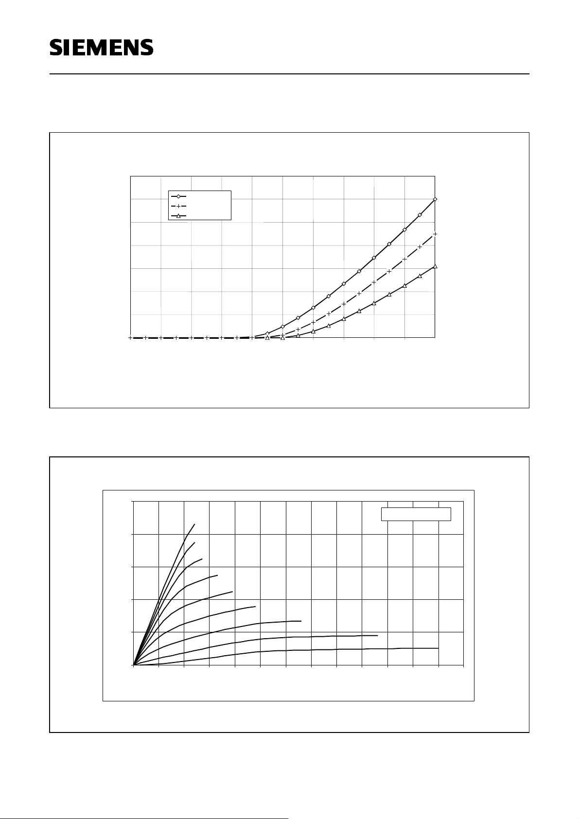
DC-ID(Vneg) characteristics – typical values of stage 1 and 2, V
High current
Medium current
Low current
-5 -4,5 -4 -3,5 -3 -2,5 -2 -1,5 -1 -0,5 0
Vneg [V]
=3V
D
0,35
0,3
0,25
0,2
0,15
0,1
0,05
0
ID
[A]
DC-Output characteristics – typical values of stage 1 and 2
0,25
Vneg=-0.25
0,2
0,15
ID [A]
0,1
0,05
0
00,511,522,5 33,5 44,555,5 66,5
-0.50 V
-0.75 V
-1.00 V
-1.25 V
-1.50 V
-1.75 V
VD [V]
Ptot=223.7m W
-2.00 V
-2.25 V
Pin 2( Vcon ) has to be open during measuring DC-characteristics
Siemens Aktiengesellschaft 4 23.07.97
Semiconductor Group 4 1998-11-01
HL HF PE GaAs
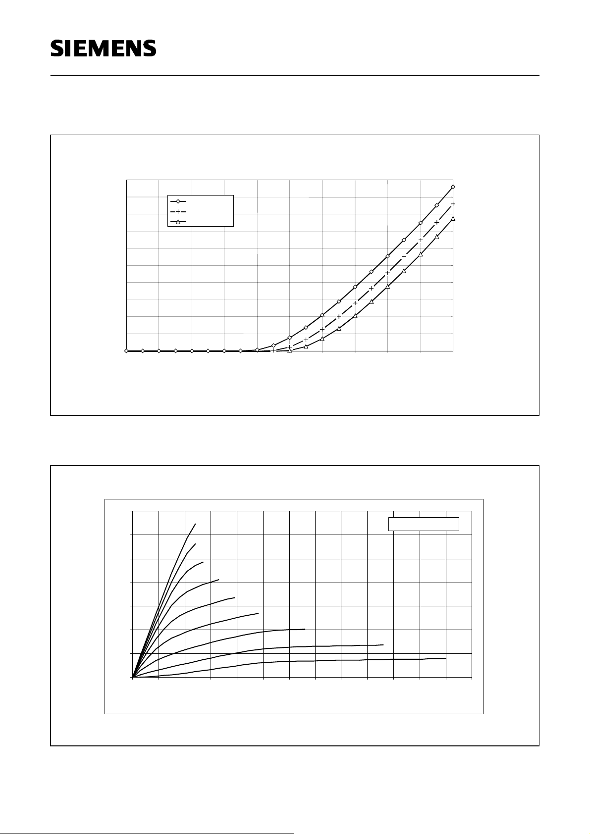
DC-ID(Vneg) characteristics – typical values of stage 3, VD=3V
CGY 184
2
High current
Medium current
Low current
-5 -4,5 -4 -3,5 -3 -2,5 -2 -1,5 -1 -0,5 0
Vneg [V]
DC-Output characteristics – typical values of stage 3
1,8
1,6
1,4
1,2
1
0,8
0,6
0,4
0,2
0
ID
[A]
1,4
Vneg=-0.25
1,2
1
0,8
ID [A]
0,6
0,4
0,2
0
0 0,5 1 1,5 2 2,5 3 3,5 4 4,5 5 5,5 6 6,5
-0.50 V
-0.75 V
-1.00 V
-1.25 V
-1.50 V
-1.75 V
VD [V]
Ptot=1.34 W
-2.00 V
-2.25 V
Pin 2( Vcon ) has to be open during measuring DC-characteristics
Siemens Aktiengesellschaft 5 23.07.97
Semiconductor Group 5 1998-11-01
HL HF PE GaAs
 Loading...