

Siemens CGY180 Datasheet
GaAs MMIC CGY 180
_________________________________________________________________________________________________________
Datasheet
* Power amplifier for DECT and PCS application
* Fully integrated 3 stage amplifier
* Operating voltage range: 2.7 to 6 V
* Overall power added efficiency 35 %
* Input matched to 50 Ω, simple output match
ESD: Electrostatic discharge sensitive device,
observe handling precautions!
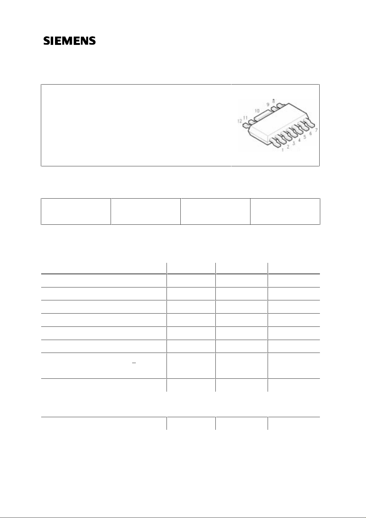
Type Marking Ordering code
(taped)
Package 1)
CGY 180 CGY 180 Q68000-A8882 MW 12
Maximum ratings
Characteristics Symbol max. Value Unit
Positive supply voltage V
Negative supply voltage 2)V
Supply current
Maximum input power
Channel temperature
Storage temperature
Total power dissipation
Ts: Temperature at soldering point
(Ts < 81 °C)
D
G
I
D
P
in,max
T
Ch
T
stg
P
tot
8V
-8 V
1.2 A
10 dBm
150 °C
-55...+150 °C
2.3 W
Pulse peak power
P
Pulse
9.5 W
Thermal Resistance
Channel-soldering point
1) Plastic body identical to SOT 223, dimensions see chapter Package Outlines
2) VG = -8V only in combination with V
Siemens Aktiengesellschaft pg. 1/15 21.02.96
HL EH PD 21
= 0V; VG = -6V while V
TR
R
thChS
TR
≠ 0V
≤30
K/W
GaAs MMIC CGY 180
_________________________________________________________________________________________________________
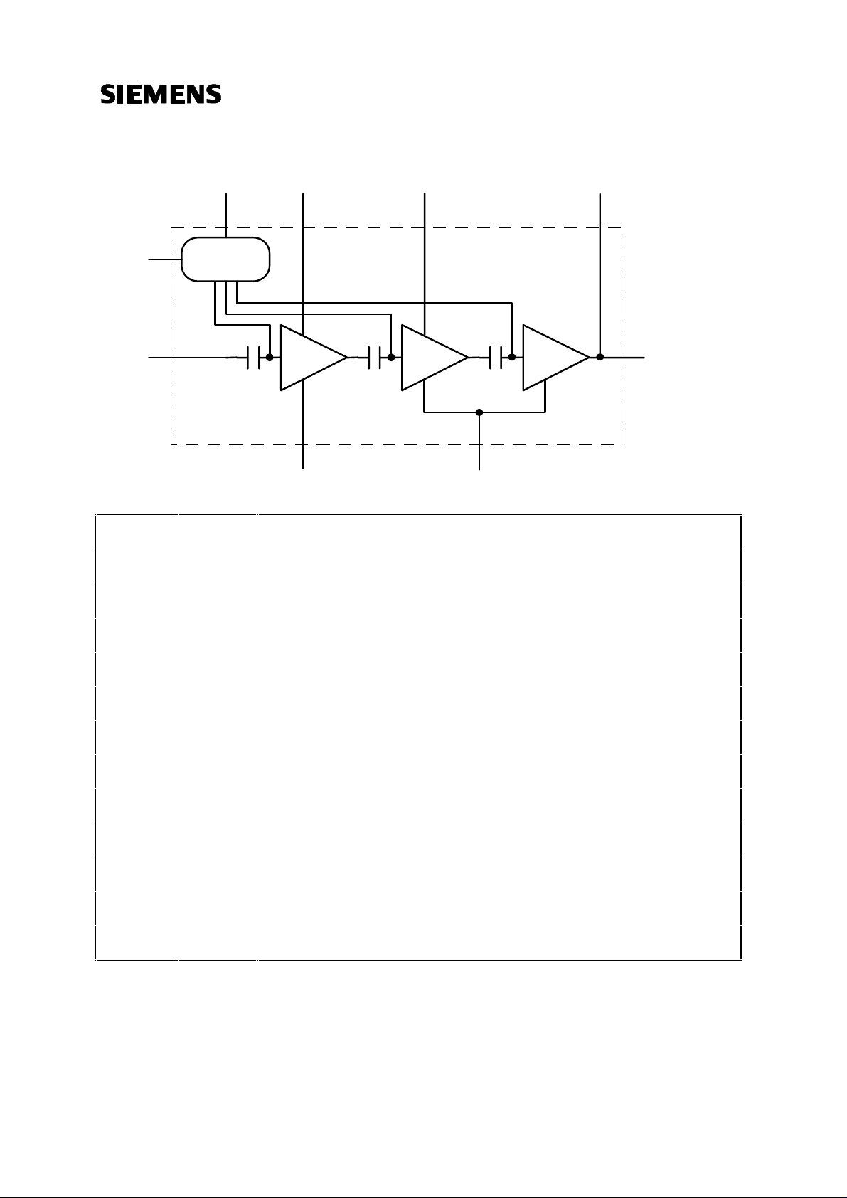
Functional Block Diagram:
VD1 VD2 VD3VG
GND1
VTR
Pin
(7)
(1)
Control
circuit
(2)
Pin # Configuration
1
2
VTR
VG
Control voltage for transmit (0V) / receive (open) mode
Negative voltage at control circuit (-4V...-8V)
(8) (9)
(6)
GND2
(3,4,5,10)
(11)
Pout
(11)
10
11
12
3
4
5
6
7
8
9
GND2
GND2
GND2
GND1
RFin
VD1
VD2
GND2
VD3, Pout
RF and DC ground of the 2nd and 3rd stage
RF and DC ground of the 2nd and 3rd stage
RF and DC ground of the 2nd and 3rd stage
RF and DC ground of the 1st stage
RF input power
Pos. drain voltage of the 1st stage
Pos. drain voltage of the 2nd stage
RF and DC ground of the 2nd and 3rd stage
Pos. drain voltage of the 3rd stage, RF output power
n.c.
Siemens Aktiengesellschaft pg. 2/15 21.02.96
HL EH PD 21
GaAs MMIC CGY 180
_________________________________________________________________________________________________________
Control circuit:
VG supply: Negative voltage (stabilization is not necessary) in the range of -4V...-8V.
VTR supply: During transmit operation: 0V., negative supply current 1mA...2.5mA.
During receive operation: not connected (shut off mode)
The operation current ID of CGY 180 is adjusted by the internal control circuit.
DC characteristics
Characteristics Symbol Conditions min typ max Unit
Drain current stage 1
stage 2
stage 3
Drain current with
active current control
Transconductance
(stage 1 - 3)
Pinch off voltage
IDSS1
IDSS2
IDSS3
ID
gfs1
gfs2
gfs3
Vp
VD=3V, VG=0V, VTR n.c. 150 220 320 mA
150 220 320 mA
675 1000 1440 mA
VD=3V, VG=-4V, VTR=0V
VD=3V, ID=90mA 80 100 140 mS
VD=3V, ID=90mA 80 100 140 mS
VD=3V, ID=400mA 360 500 630 mS
VD=3V, ID<170µA
(all stages)
290 450 650 mA
-3.8 -2.8 -1.8 V
Siemens Aktiengesellschaft pg. 3/15 21.02.96
HL EH PD 21
GaAs MMIC CGY 180
_________________________________________________________________________________________________________
Electrical characteristics
(TA = 25°C , f=1.89 GHz, ZS=ZL=50 Ohm, VD=3.0V, VG=-4V, VTR pin connected to
ground, unless otherwise specified)
Characteristics Symbol min typ max Unit
Supply current
Pin = 0 dBm
Negative supply current
(transmit operation)
Shut-off current
VTR n.c.
Negative supply current
(shut off mode, VTR pin n.c.)
Gain
P
= -20dBm
Output Power
P
= 0 dBm
Output Power
VD=5V; P
= 0 dBm
Overall Power added Efficiency
P
= 0 dBm
Harmonics
VD=3V; (P
Harmonics
VD=5V; (P
Input VSWR V
(P
=0dBm)
=27dBm)
(P
=0dBm)
=30dBm)
D=3V;
2f
3f
2f
3f
0
0
0
0
Third order intercept point
VD=3V; pulsed with a duty cycle of 10%;
f
=1.8900GHz; f2=1.891728GHz;
1
Third order intercept point
VD=4.8V; pulsed with a duty cycle of 10%;
f
=1.8900GHz; f2=1.891728GHz;
1
Load mismatch
Pin=0dBm, VD≤6V, Z
Load VSWR = 20:1 for all phase,
VTR=0V, VG=-4V
=50 Ohm,
I
DD
I
I
I
G
P
P
η
G
D
G
o
o
-
-
-
-
- 450 - mA
- 1 2.5 mA
- 50 180 µA
-1050µA
28 30 - dB
25.5 27 - dBm
- 30 - dBm
30 35 - %
-
-
-
-
-
-
-
-
-28
-25
-25
-22
- - 2 : 1 2.5 : 1 -
IP
IP
3
3
-
- 33.5 - dBm
- 38.5 - dBm
No module damage
for 10 sec.
dBc
dBc
-
Stability
Pin=0dBm, VD=2-7V, Z
Load VSWR = 3:1 for all phase,
VTR=0V, VG=-4V
Siemens Aktiengesellschaft pg. 4/15 21.02.96
HL EH PD 21
=50 Ohm,
-
All spurious output
-
more than 60 dB below
desired signal level
GaAs MMIC CGY 180
_________________________________________________________________________________________________________
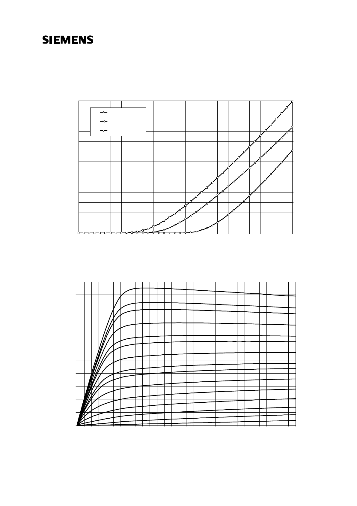
DC - characteristics
Input characteristics - typical measured values of stage 1 and 2 , VD1 or VD2=3V
0,26
low current
medium current
high current
0,24
0,22
0,2
0,18
0,16
0,14
0,12
0,1
0,08
0,06
0,04
ID[A]
-4 -3,8 -3,6 -3,4 -3,2 -3 -2,8 -2,6 -2,4 -2,2 -2 -1,8 -1,6 -1,4 -1,2 -1 -0,8 -0,6 -0,4 -0,2 0
VG[V]
Output characteristics - typical measured values of stage 1 and 2
0,22
0,2
0,18
0,16
0,14
0,12
ID[A]
0,1
0,08
0,06
0,04
0,02
0
0 0,2 0,4 0,6 0,8 1 1,2 1,4 1,6 1,8 2 2,2 2,4 2,6 2,8 3 3,2 3,4 3,6 3,8 4 4,2 4,4 4,6 4,8 5 5,2 5,4 5,6 5,8 6
VD[V]
0,02
0
0V
-0.2V
-0.3V
-0.5V
-0.7V
-0.8V
-1.0V
-1.2V
-1.3V
-1.5V
-1.7V
-1.9V
-2.1V
-2.3V
-2.5V
Siemens Aktiengesellschaft pg. 5/15 21.02.96
HL EH PD 21
 Loading...