

Siemens CGY121B Datasheet
GaAs MMIC
CGY 121 B
Preliminary Data
l
Variable gain amplifier
(MMIC-Amplifier) fo r mobile commun ication
l
Gain Control range over 50dB
l
Positive Control Voltage
l
50Ω input and output matched
l
Low power consumption
l
Operating voltage range: 2.7 to 6 V
l
Frequency range 800 MHz ... 2.5 GHz
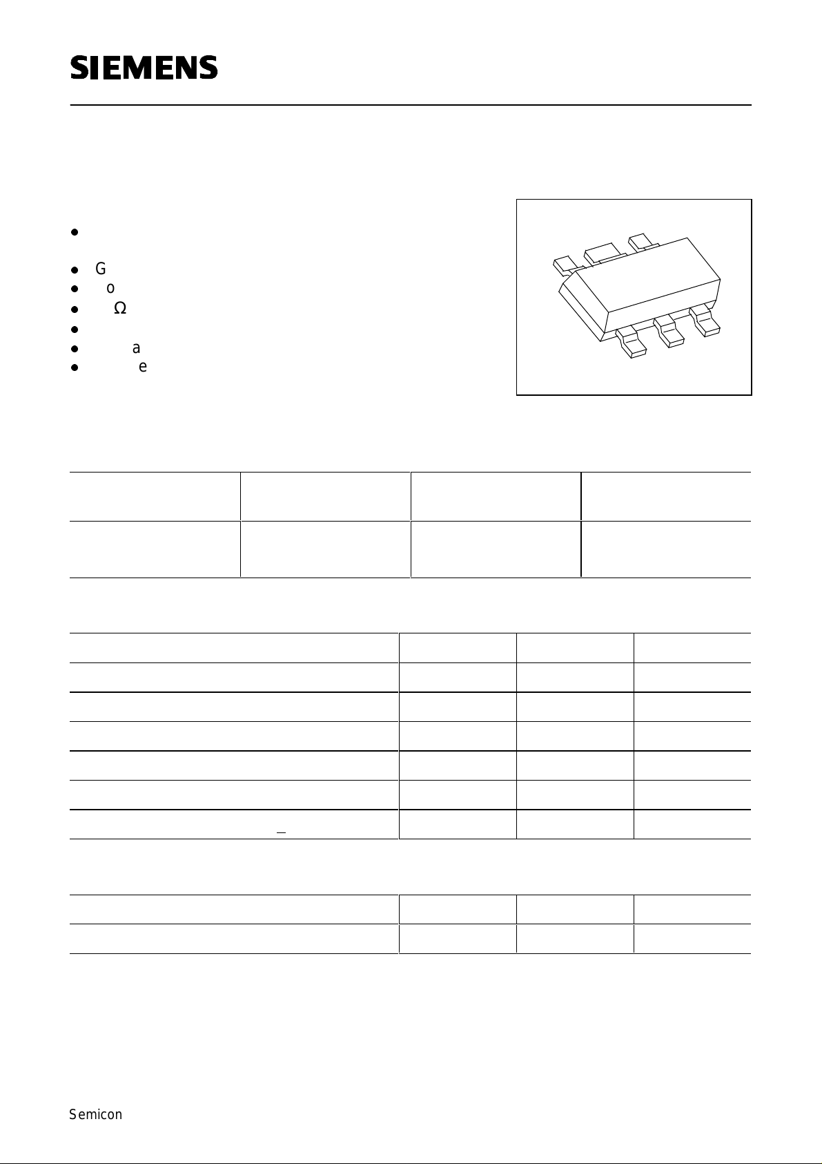
Vcontrol
6
RF-GND
5
RF-in; -Vg
4
Vd2; RF-out
3
2
1
RF-GND
Vd1
ESD: Electrostatic discharge sensitive device, *
observe handling precautions!
Type Marking Ordering code
Package
1)
(taped)
CGY 121 B Y0S Q62702-G0071 MW-6
)
Maximum ratings
Characteristics Symbol Unit
Drain voltage
Neg. supply voltage
Pos. control voltage
Channel temperature
Storage temperature range
Total power dissipation (TS < 81°C)
2)
V
D
V
G
Vcon
T
Ch
T
stg
P
tot
8V
-8 V
4V
150 °C
-55...+150 °C
550 mW
Thermal resistance
Characteristics Symbol Unit
Channel-soldering point (GND)
1)
Dimensions see page 9.
2)
Please care for sufficient heat dissipation on the pcb!
R
thChS
125 K/W
*) Pin-out changed compared to CGY120: 180° rotation
Siemens Aktiengesellschaft 1 04.08.98
HL HF PE GaAs/HB
Semiconductor Group 1 1998-11-01Semiconductor Group 1 1998-11-01
CGY 121 B
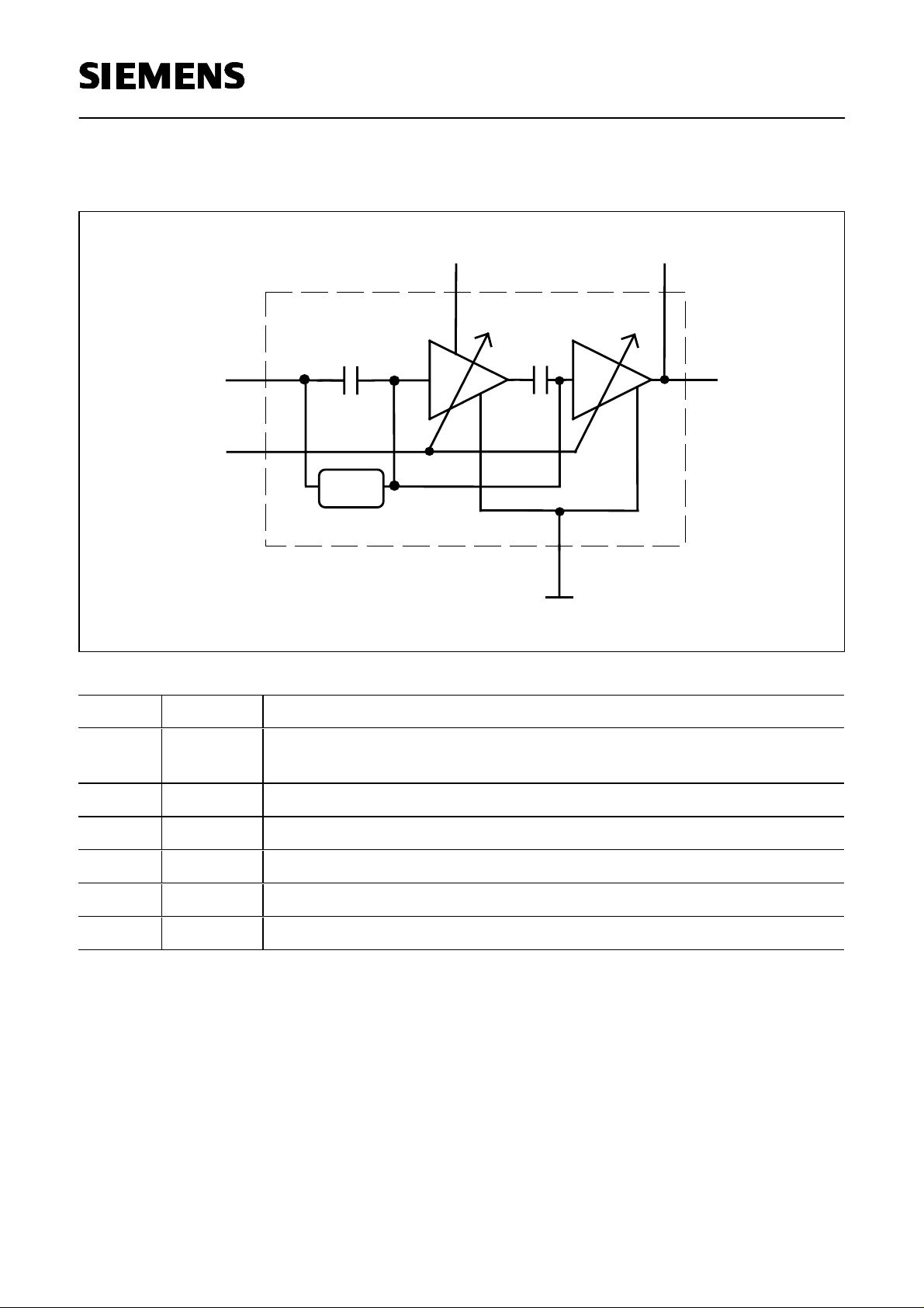
Functional block diagram:
Pin / -VG(4)
Vcon (6)
Control
Circuit
Pin # Configuration
VD1 (3)
GND (2, 5)
VD2 (1)
Pout (1)
1
VD2 /
Drain voltage 2nd stage / RF-0utput
Pout
2
3
4
5
6
RF-Gnd
VD1
VG / Pin
RF-Gnd
Vcontrol
Drain voltage 1st stage
Negative voltage at current control circuit (-4V) / RF-Input
Positive voltage for gain control (0V....3V)
Siemens Aktiengesellschaft 2 04.08.98
HL HF PE GaAs/HB
Semiconductor Group 2 1998-11-01Semiconductor Group 2 1998-11-01
CGY 121 B
Electrical characteristics
(
T
= 25°C, f = 900 MHz, Vg = -4V, RS = RL = 50 Ω unless otherwise specified)
A
Characteristics Symbol min typ max Unit
Power Gain
G
- 21.5 - dB
Vd=5V; I=70mA; Vcon=3V
Input return loss
RL
in
-15-dB
Vd=5V; I=70mA; Vcon=3V
Output return loss
RL
out
-11-dB
Vd=5V; I=70mA; Vcon=3V
Gain Control Range
dG
-55-dB
Vcon=3 V ... 0V; Vd=5V; I=70mA
1dB gain compression
P
1
dB
-16-dBm
Vd=5V; I=70mA; Vcon=3V
Electrical characteristics
(
T
= 25°C, f = 1800 MHz, Vg=-4V, RS = RL = 50 Ω unless otherwise specified)
A
Characteristics Symbol min typ max Unit
Power Gain
G
- 19.5 - dB
Vd=5V; I=70mA; Vcon=3V
Input return loss
RL
in
-10-dB
Vd=5V; I=70mA; Vcon=3V
Output return loss
RL
out
-8-dB
Vd=5V; I=70mA; Vcon=3V
Gain Control Range
dG
-55-dB
Vcon=3 V ... 0V; Vd=5V; I=70mA
1dB gain compression
P
1
dB
-16-dBm
Vd=5V; I=70mA; Vcon=3V
DC characteristics
Characteristics Symbol min typ max Unit
Gate current (Pin 4)
Ig - 1.0 - mA
Vg=-4V
Control current (Pin 6)
Ic - 0.5 - mA
Vg=-4V; Vcon=0V...3V
Supply current
Id - 70 - mA
Vg = -4V; Vcon = 3V
Siemens Aktiengesellschaft 3 04.08.98
HL HF PE GaAs/HB
Semiconductor Group 3 1998-11-01Semiconductor Group 3 1998-11-01
 Loading...