

Siemens CGY0918 Datasheet
GaAs MMIC
l
Dual band GSM/PCN power amplifier
l
35dBm / 34dBm output power at 3.5 V
l
Two amplifiers in a single package
l
Power ramp control
ESD: Electrostatic discharge sensitive device,
observe handling precautions!
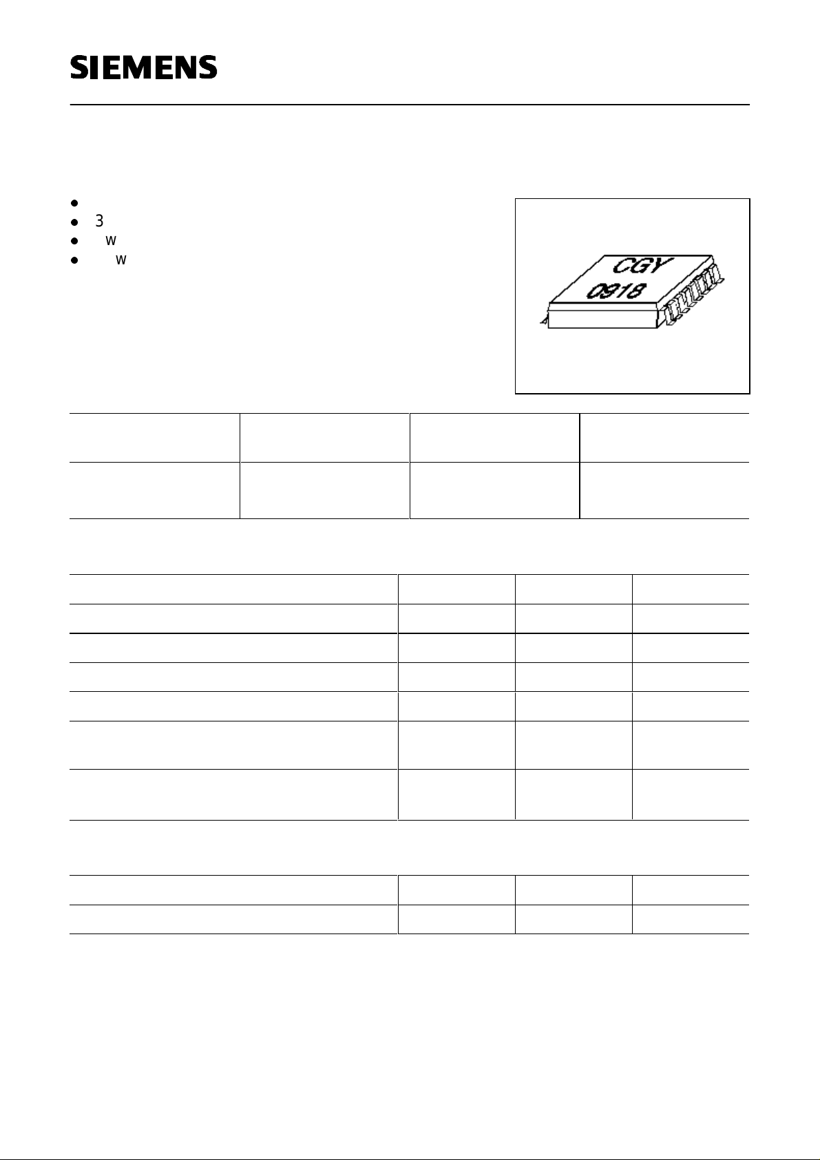
CGY 0918
Type Marking Ordering code
Package
(taped)
CGY 0918 CGY 0918 Q62702G0077 MW 16
Maximum ratings
Characteristics Symbol max. Value Unit
Positive supply voltage V
Supply current
Channel temperature
Storage temperature
Pulse peak power dissipation
T
T
P
Pulse
duty cycle 12.5%, ton=0.577ms
Total power dissipation
(Ts ≤ 80 °C)
P
Ts: Temperature at soldering point
D
I
D
Ch
stg
tot
9V
4A
150 °C
-55...+150 °C
tbd W
tbd W
Thermal Resistance
Characteristics Symbol max. Value Unit
Channel-soldering point
Siemens Aktiengesellschaft 1 23.07.98
Semiconductor Group 1 1998-11-01
R
thChS
tbd K/W
HL HF PE GaAs
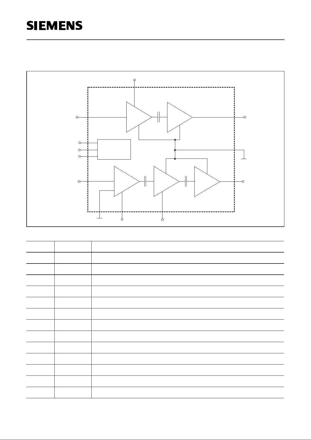
Functional block diagramm:
CGY 0918
G_VD1
CGY0918
G_IN
G_Control
P_Control
Vneg
P_IN
current
control circuit
P_GND1
Pin # Name Configuration
1
P_IN
RF input PCN
G_OUT
GND
P_OUT
2
3
4
5,6,7,8
9
10
11
12
13
14
15,16
(17)
Siemens Aktiengesellschaft 2 23.07.98
Semiconductor Group 2 1998-11-01
P_GND1
P_VD1
P_VD2
P_OUT
G_IN
G_Control
P_Control
Vneg
n.c.
G_VD1
G_OUT
GND2
Ground 1st stage PCN
Drain 1st stage PCN
Drain 2nd stage
RF output PCN and drain 3rd stage
RF input GSM
Power control GSM
Power control PCN
Negative voltage for current control circuit
Drain 1st stage GSM
RF output GSM and drain 2nd stage
Ground (backside of MW16 package)
HL HF PE GaAs
 Loading...