

Siemens CFY30 Datasheet
GaAs FET CFY 30
________________________________________________________________________________________________________
D a t a s h e e t
* Low noise ( F
= 1.4 dB @ 4 GHz )
*High gain ( 11.5 dB typ. @ 4 GHz )
*For oscillators up to 12 GHz
*For amplifiers up to 6 GHz
*Ion implanted planar structure
* Chip all gold metallization
* Chip nitride passivation
ESD: Electrostatic discharge sensitive device,
observe handling precautions!
Type Marking Ordering code
(tape and reel)
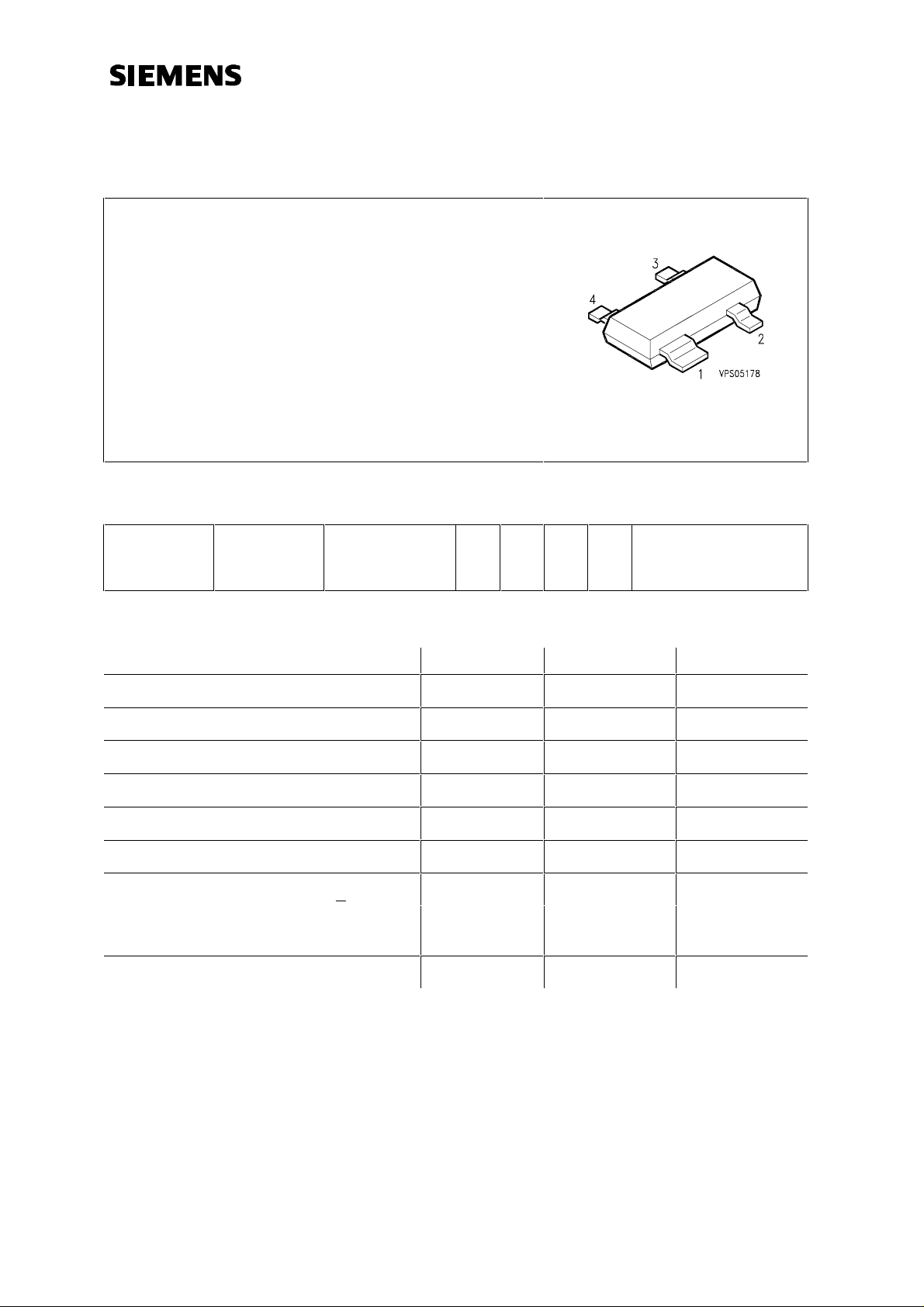
Pin Configuration
1 2 3 4
Package 1)
CFY 30 A2 Q62703-F97 S D S G SOT-143
Maximum ratings Symbol Value Unit
Drain-source voltage
Drain-gate voltage
Gate-source voltage
Drain current
Channel temperature
Storage temperature range
Total power dissipation (TS < 70°C)
2)
V
V
V
T
T
P
DS
DG
GS
I
D
Ch
stg
tot
-4 ... +0.5 V
80 mA
150 °C
-40...+150 °C
250 mW
Thermal resistance
Channel-soldering point
1) Dimensions see chapter Package Outlines
2) TS is measured on the source 1 lead at the soldering point to the PCB.
2)
R
thChS
<320 K/W
5V
7V
Siemens Aktiengesellschaft pg. 1/6 11.01.1996
HL EH PD 21
GaAs FET CFY 30
________________________________________________________________________________________________________
Electrical characteristics at
T
= 25°C, unless otherwise specified
A
Characteristics Symbol min typ max Unit
Drain-source saturation current
VDS = 3.5 V, VGS = 0 V
Pinch-off voltage
VDS = 3.5 V ID = 1 mA
Transconductance
VDS = 3.5 V I
= 15 mA
D
Gate leakage current
VDS = 3.5 V ID = 15 mA
Noise figure
V
= 3.5 V I
f = 6 GHz
= 15 mA f = 4 GHz
V
I
mA
20 50 80
V
-0.5 -1.3 -4.0
g
mS
20 30 -
I
µA
- 0.1 2
F
-
-
1.4
2.0
1.6
-
dB
Associated gain
V
= 3.5 V I
f = 6 GHz
= 15 mA f = 4 GHz
Maximum available gain
VDS = 3.5 V ID = 15 mA f = 6 GHz
Maximum stable gain
VDS = 3.5 V ID = 15 mA f = 4 GHz
Power output at 1 dB compression
VDS = 4 V ID = 30 mA f = 6 GHz
G
MAG
MSG
P
10
-
11.5
8.9
-
-
- 11.2 -
- 14.4 -
-16-
dB
dB
dB
dBm
Siemens Aktiengesellschaft pg. 2/6 11.01.1996
HL EH PD 21
 Loading...