

Siemens BUP213 Datasheet
IGBT
Preliminary data
• Low forward voltage drop
• High switching speed
• Low tail current
• Latch-up free
• Avalanche rated
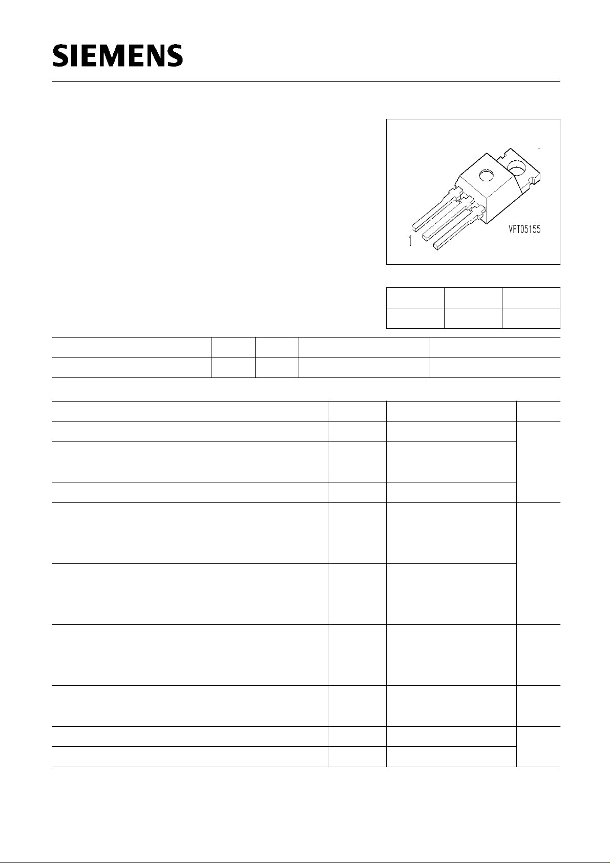
BUP 213
Pin 1 Pin 2 Pin 3
G C E
Type
V
CE
I
C
Package Ordering Code
BUP 213 1200V 32A TO-220 AB Q67040-A4407-A2
Maximum Ratings
Parameter Symbol Values Unit
Collector-emitter voltage
Collector-gate voltage
R
= 20 k
GE
Ω
Gate-emitter voltage
DC collector current
T
= 25 °C
C
T
= 90 °C
C
Pulsed collector current,
T
= 25 °C
C
T
= 90 °C
C
t
= 1 ms
p
Avalanche energy, single pulse
V
CE
V
CGR
V
GE
I
C
I
Cpuls
E
AS
1200 V
1200
± 20
A
32
20
64
40
mJ
I
= 15 A,
C
L
= 200 µH,
V
CC
T
= 50 V,
= 25 °C
j
R
GE
= 25
Power dissipation
T
= 25 °C
C
Chip or operating temperature
Storage temperature
Semiconductor Group
Ω
22
P
tot
W
200
T
j
T
stg
-55 ... + 150 °C
-55 ... + 150
1 Nov-30-1995
BUP 213
Maximum Ratings
Parameter Symbol Values Unit
DIN humidity category, DIN 40 040 - E IEC climatic category, DIN IEC 68-1 - 55 / 150 / 56
Thermal Resistance
IGBT thermal resistance, chip case
R
thJC
≤
0.63 K/W
Electrical Characteristics, at Tj = 25 °C, unless otherwise specified
Parameter Symbol Values Unit
min. typ. max.
Static Characteristics
Gate threshold voltage
V
=
GE
V
CE, IC
= 0.35 mA
Collector-emitter saturation voltage
V
V
V
V
GE
GE
GE
GE
= 15 V,
= 15 V,
= 15 V,
= 15 V,
I
= 15 A,
C
I
= 15 A,
C
I
= 30 A,
C
I
= 30 A,
C
T
= 25 °C
j
T
= 125 °C
j
T
= 25 °C
j
T
= 125 °C
j
Zero gate voltage collector current
V
GE(th)
V
CE(sat)
I
CES
4.5 5.5 6.5
-
-
-
-
2.7
3.3
3.4
4.3
3.2
3.9
-
-
V
mA
V
= 1200 V,
CE
V
GE
= 0 V,
T
Gate-emitter leakage current
V
= 25 V,
GE
V
CE
= 0 V
AC Characteristics
Transconductance
V
= 20 V,
CE
I
= 15 A
C
Input capacitance
V
= 25 V,
CE
V
= 0 V, f = 1 MHz
GE
Output capacitance
V
= 25 V,
CE
V
= 0 V, f = 1 MHz
GE
Reverse transfer capacitance
V
= 25 V,
CE
Semiconductor Group
V
= 0 V, f = 1 MHz
GE
= 25 °C
j
- - 0.8
I
GES
nA
- - 100
g
fs
S
- 12 -
C
iss
pF
- 1000 1350
C
oss
- 150 225
C
rss
- 70 100
2 Nov-30-1995

BUP 213
Electrical Characteristics, at Tj = 25 °C, unless otherwise specified
Parameter Symbol Values Unit
min. typ. max.
Switching Characteristics, Inductive Load at
Turn-on delay time
V
R
CC
Gon
= 600 V,
= 82
Ω
V
GE
Rise time
V
R
CC
Gon
= 600 V,
= 82 Ω
V
GE
Turn-off delay time
V
R
CC
Goff
= 600 V,
= 82 Ω
V
GE
Fall time
V
R
CC
Goff
= 600 V,
= 82 Ω
V
GE
= 15 V,
= 15 V,
= -15 V,
= -15 V,
I
= 15 A
C
I
= 15 A
C
I
= 15 A
C
I
= 15 A
C
t
d(on)
t
r
t
d(off)
t
f
T
= 125 °C
j
- 70 100
- 45 70
- 400 530
- 70 95
ns
Semiconductor Group
3 Nov-30-1995
 Loading...