

Siemens BSP78 Datasheet
Preliminary data
Smart Lowside Power Switch
HITFETBSP 78
Features
• Logic Level Input
• Input Protection (ESD)
•
Thermal shutdown with
auto restart
•
Overload protection
Product Summary
Drain source voltage
V
On-state resistance R
Nominal load current I
Clamping energy mJE
DS
DS(on)
D(Nom)
AS
• Short circuit protection
• Overvoltage protection
•
Current limitation
• Analog driving possible
Application
• All kinds of resistive, inductive and capacitive loads in switching or linear
applications
• µC compatible power switch for 12 V and 24 V DC applications
• Replaces electromechanical relays and discrete circuits
V40
50 mΩ
3 A
500
General Description
N channel vertical power FET in Smart SIPMOS technology. Fully protected by embedded
protection functions.
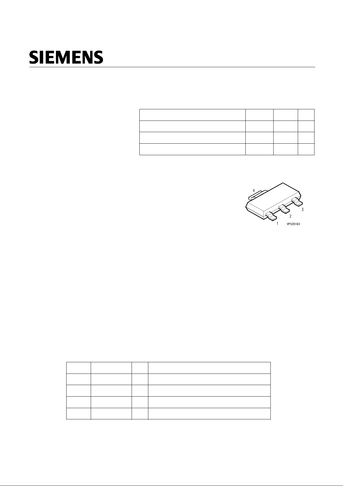
Pin Symbol Function
1 IN Input
2 DRAIN Output to the load
3 SOURCE Ground
TAB DRAIN Output to the load
Semiconductor Group
Jan-15-1998Page 1
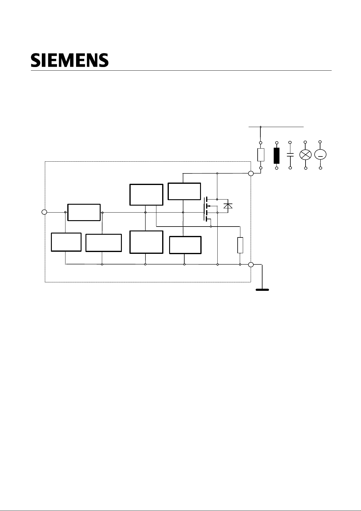
Block Diagram
Preliminary data
BSP 78
V
bb
+
IN
Gate-Driving
ESD
Unit
protection
Overload
Current
limitation
Over-
temperature
protection
Overvoltage
protection
Short circuit
Short circuit
protection
protection
Drain
Source
HITFET
LOAD
M
Semiconductor Group
Jan-15-1998Page 2
Preliminary data
Maximum Ratings at Tj = 25°C, unless otherwise specified
Parameter Value UnitSymbol
BSP 78
Drain source voltage
Drain source voltage for
V
DS
DS(SC)
40V
short circuit protection
Continuous input voltage V
Peak input voltage (I
Operating temperature T
Storage temperature T
Power dissipation,
Unclamped single pulse inductive energy
lectrostatic discharge voltage (Human Body Model)
E
≤ 2 mA) V
IN
T
= 85 °C
C
F)
IN
IN(peak)
j
stg
P
tot
E
AS
ESD
-0.2 ... +10
-0.2 ...
V
DS
-40 ...+150
-55 ...+150
500 mJ
2000V
according to MIL STD 883D, method 3015.7 and
EOS/ESD assn. standard S5.1 - 1993
DIN humidity category, DIN 40 040
E
IEC climatic category; DIN IEC 68-1 40/150/56
V40
°C
W1.7
kV
Thermal resistance
junction - ambient:
@ min. footprint
@ 6 cm2 cooling area
F)
junction-soldering point: R
1
not tested, specified by design
2
Device on 50mm+50mm*1.5mm epoxy PCB FR4 with 6 cm2 (one layer, 70µm thick) copper area for Drain
connection. PCB is vertical without blown air.
Semiconductor Group
R
thJA
thJS
125
72
17 K/W
Jan-15-1998Page 3
K/W
 Loading...