

Siemens BSP75A Datasheet
Smart Lowside Power Switch
)
)
)
Preliminary data sheet HITFET® BSP 75A
Features
•
Logic Level Input
•
Input protection (ESD)
•
Thermal shutdown (with restart)
•
Overload protection
•
Short circuit protection
•
Overvoltage protection
•
Current limitation
Product Summary
Continuous drain source voltage V
On-state resistance
Current limitation
Load current (ISO)
Clamping energy
R
I
I
E
DS
DS(ON
D(lim
D(ISO
AS
55 V
550
mΩ
1A
0.7 A
550 mJ
Application
•
All kinds of resistive, inductive and capacitive loads in switching applications
•
µC compatible power switch for 12 V and 24 V DC applications
•
Replaces electromechanical relays and discrete circuits
General Description
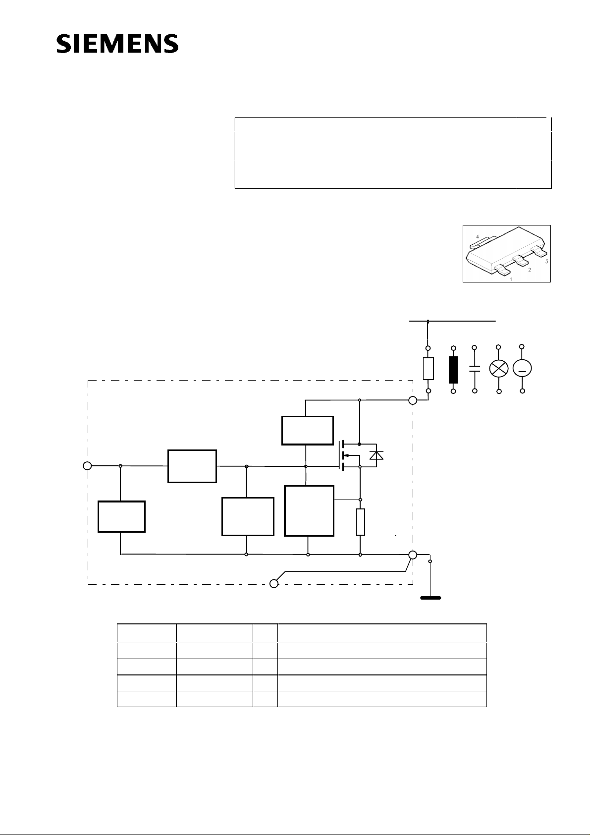
N channel vertical power FET in Smart Power Technology. Fully protected by embedded protection functions.
V
bb
+
LOAD
M
Drain
Overvoltage
protection
1
IN
ESD
HITFET
Pin Symbol Function
1 IN Input
2 DRAIN Output to the load
3 SOURCE Ground
TAB SUBSTRATE Internally connected to source (pin 3)
dv/dt
limitation
Over-
temperature
protection
4
Short circuit
protection
Short circuit
Current
protection
limitation
Source
2
3
Semiconductor Group Page 1 of 9 1998-02-04
Preliminary data sheet HITFET® BSP 75A
)
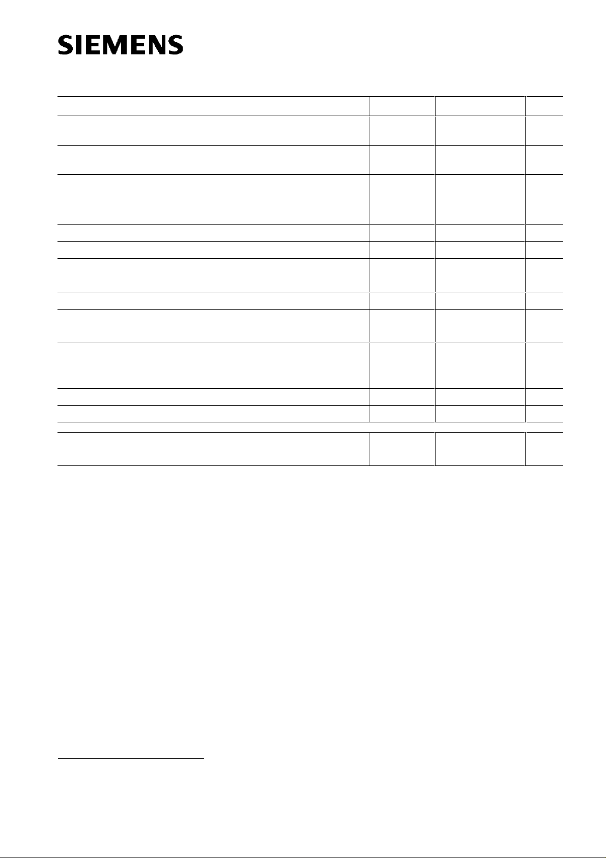
Maximum Ratings at Tj=25°C unless otherwise specified
Parameter Symbol Values Unit
Continuous drain source voltage
(overvoltage protection see page 4)
Drain source voltage for
short circuit protection
Load dump protection
1
)
R
I
R
=2 Ω;
I
=2 Ω;
t
=400ms; IN=low or high (8V)
d
t
=400ms; IN=high (8V)
d
V
LoadDump
=
U
+
U
;
U
S
=13.5 V
P
R
R
L
L
=50 Ω
=22 Ω
P
Continuous input voltage
Peak input voltage
Operating temperature range
Storage temperature range
Power dissipation (DC)
Unclamped single pulse inductive energy
I
D(ISO
= 0.7 A
Electrostatic discharge voltage (Human Body Model)
according to MIL STD 883D, method 3015.7 and
EOS/ESD assn. standard S5.1 - 1993
DIN humidity category, DIN 40 040 E
IEC climatic category, DIN IEC 68-1 40/150/56
V
DS
V
DS
V
LoadDump
V
IN
V
IN
T
j
T
stg
P
tot
E
AS
V
ESD
55 V
32 V
2
)
V
80
47
-0.2 ... +10 V
-0.2 ... +20 V
-40 ...+150
°C
-55 ...+150
1.8 W
550 mJ
4000 V
Thermal resistance junction soldering point:
junction - ambient
3
R
thJS
)
:
R
thJA
≤10
≤70
K/W
1
)
R
=internal resistance of the load dump test pulse generator LD200
I
2
)
V
LoadDump
3
)
Device on epoxy pcb 40mm x 40 mm x 1.5mm with 6cm
is setup without DUT connected to the generator per ISO 7637-1 and DIN 40 839.
2
copper area for pin 4 connection
Semiconductor Group Page 2 1998-02-04
Preliminary data sheet HITFET® BSP 75A
V
V
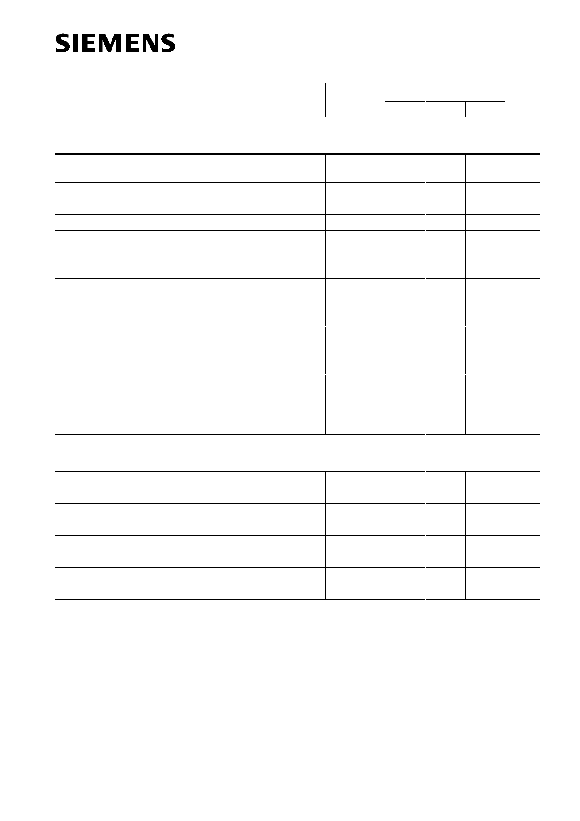
Electrical Characteristics
Parameter and Conditions Symbol Values Unit
at Tj = 25 °C, unless otherwise specified
Static Characteristics
min typ max
Drain source clamp voltage
I
= 10 mA
D
T
=-40...+150°C:
j
Off state drain current
V
= 0 V,
IN
Input threshold voltage
Input current normal operation,
V
IN = 5 V current limitation mode, ID=ID(lim):
V
DS
= 32 V
I
= 10 mA
D
T
=-40...+150°C:
j
I
D<ID(lim):
after thermal shutdown,
On-state resistance
ID = 0.7 A, V
IN
= 5 V
T
j
T
=150°C:
j
On-state resistance
ID = 0.7 A, V
= 10 V
IN
T
j
T
=150°C:
j
Nominal load current(ISO 10483)
V
IN = 10 V,
V
= 0.5 V,
DS
T
= 85°C
S
Current limit
= 10 V,
IN
= 12 V
DS
I
D=0 A:
=25°C:
=25°C:
V
DS(AZ)
I
DSS
V
IN(th)
I
IN(1)
I
IN(2)
I
IN(3)
R
DS(on)
R
DS(on)
I
D(ISO)
I
D(lim)
55 -- 70 V
-- -- 5 µA
2 2.5 3 V
--
--
1000
--
--
--
--
100
200
1500
550
850
475
750
200
300
2000
675
1350
550
1000
0.7 -- -- A
1 1.5 1.9 A
µA
mΩ
mΩ
Dynamic characteristics
Turn-on time
R
= 22 Ω, VIN= 0 to 10 V, Vbb= 12 V
L
Turn-off time
R
= 22 Ω, VIN= 10 to 0 V, Vbb= 12 V
L
V
to 90%
IN
V
to 10%
IN
I
D
I
D
Slew rate on 70 to 50% Vbb:
R
= 22 Ω, V
L
= 0 to 10 V, V
IN
bb
= 12 V
Slew rate off 50 to 70% Vbb:
R
= 22 Ω, VIN= 10 to 0 V, Vbb= 12 V
L
:
t
on
:
t
off
-d
V
/dt
DS
on
d
V
/dt
DS
off
-- 10 20 µs
-- 10 20 µs
-- 4 10 V/µs
-- 4 10 V/µs
Semiconductor Group Page 3 1998-02-04
 Loading...