

Siemens BSP350 Datasheet
Mini PROFET® BSP 350
)
MiniPROFET
•
High-side switch
•
Short-circuit protection
•
Overtemperature protection with hysteresis
•
Overload protection
•
Overvoltage protection
•
Reverse battery protection
•
Switching inductive load
•
Clamp of negative output voltage with inductive loads
•
Maximum current internally limited
Package: SOT 223
Type
BSP 350
)
1
Ordering code
Q67000-S227
Pins:
Maximum Ratings
Parameter Symbol Values Unit
Supply voltage
Load current self-limited
Maximum current through input pin (DC)
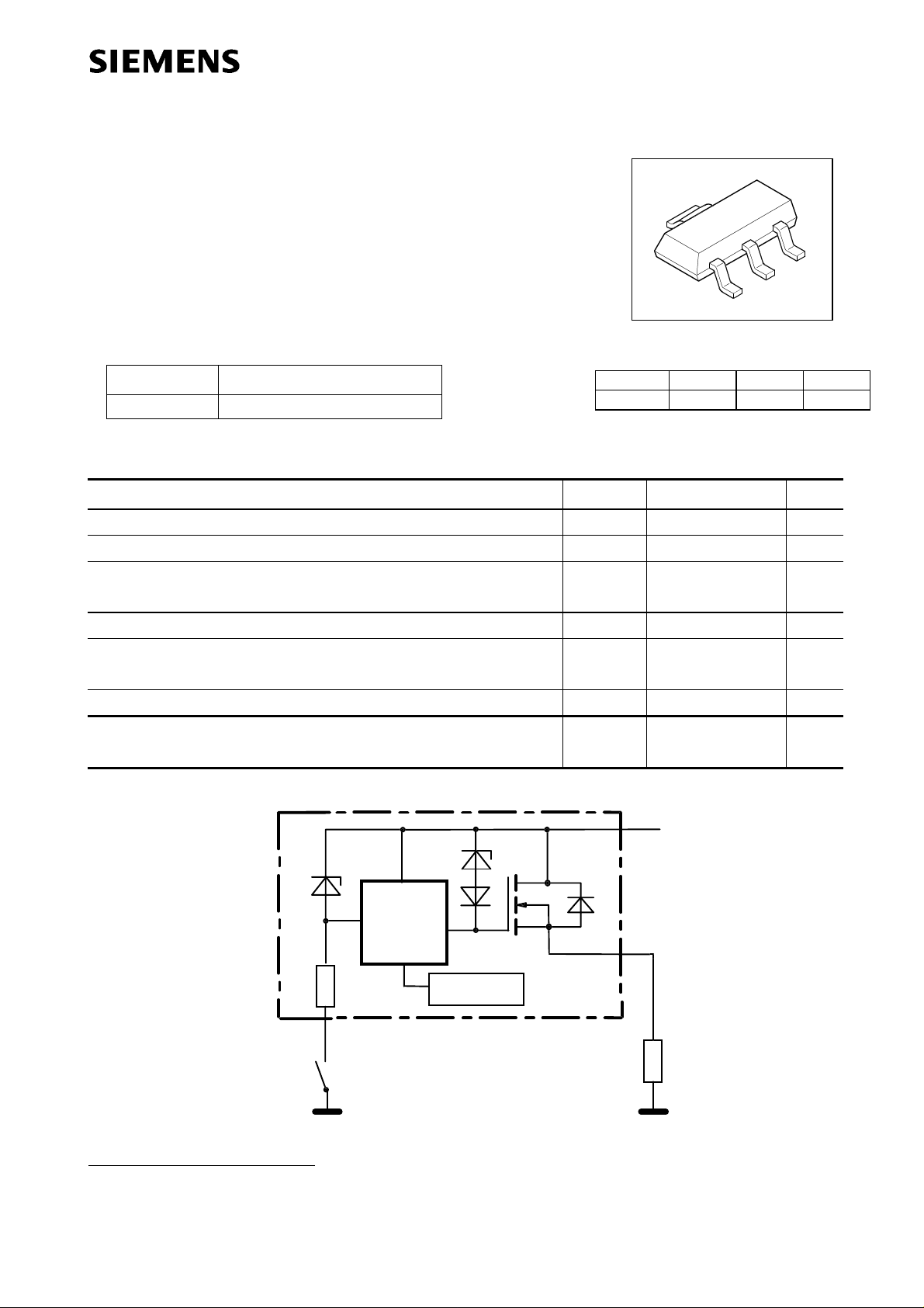
see internal circuit diagram
Inductive load switch-off energy dissipation
Operating temperature range
Storage temperature range
Max. power dissipation (DC)
2)
T
= 25 °C
A
Thermal resistance chip - soldering point:
chip - ambient:
V
bb
I
L
I
IN
E
AS
T
j
T
stg
P
tot
R
thJS
)
2
R
thJA
4
3
2
1
123
IN V
bb
OUT V
50 V
I
L(SC
±15 mA
5mJ
-40 ...+150
°C
-55 ...+150
1.7 W
1772K/W
4
bb
A
+ V
bb
2/4
Control
Circuit
R
IN
1
IN
GND
)
1
For 12 V applications only. Reverse load current only limited by connected load.
2)
BSP 350 on epoxy pcb 40 mm x 40 mm x 1.5 mm with 6 cm2 copper area for Vbb connection
Temperature
Sensor
OUT
3
R
L
Semiconductor Group 1 04.97

BSP 350
Electrical Characteristics
Parameter and Conditions Symbol Values Unit
T
at
= 25 °C,
j
Load Switching Capabilities and Characteristics
On-state resistance (pin 2 to 3)
I
= 0.07 A, pin 1 = GND
L
Nominal load current (pin 2 to 3)
ISO Standard:
T
= 85 °C
S
Turn-on time to 90%
Turn-off time to 10%
R
= 270 Ω
L
Slew rate on
10 to 30%
Slew rate off
70 to 40%
V
= 13.5V unless otherwise specified
bb
V
= 6 V,
bb
V
V
OUT
OUT
VON = V
R
= 270 Ω
,
L
R
,
= 270 Ω
L
bb
-
V
OUT
= 0.5 V
T
= 25°C
j
T
= 150°C
j
T
= 25°C
j
V
V
OUT
OUT
R
ON
I
L(ISO)
t
on
t
off
dV /dt
-dV/dt
on
off
min typ max
--
--
--
0.07 -- -- A
--
--
60
70
4
8
5
10
10
100
5
µs
140
-- 4 6 V/µs
-- 2 6
Ω
Input
OFF state input current
R
= 270 Ω,
L
V
OUT
≤ 0,1V
T
= - 40...+150°C
j
ON state input current, (pin 1 grounded)
T
= - 40...+150°C
j
Operating Parameters
)
Operating voltage (pin 1 grounded)
T
= - 40...+150°C
j
4
Leakage current (pin 2 to 3, pin 1 open)
)
3
T
= 25°C
j
T
=150°C
j
I
IN(off)
I
IN(on)
V
bb(on)
I
bb(off)
-- -- 0.05 mA
-- 0.3 1 mA
4.9 -- 45 V
--
--
1.2
1
10
10
A
µ
)
3
Driver circuit must be capable to drive currents >1mA.
)
4
Below Vbb=4.5 V typ. without chargepump, V
≈ Vbb - 2 V
out
Semiconductor Group 2
 Loading...