

Siemens BSP320S Datasheet
BSP 320 S
SIPMOS
Small-Signal Transistor
®
• N channel
• Enhancement mode
• Avalanche rated
• V
Type
= 2.1 ... 4.0 V
GS(th)
V
DS
I
D
R
DS(on)
BSP 320 S 60 V 2.9 A 0.12
Ω
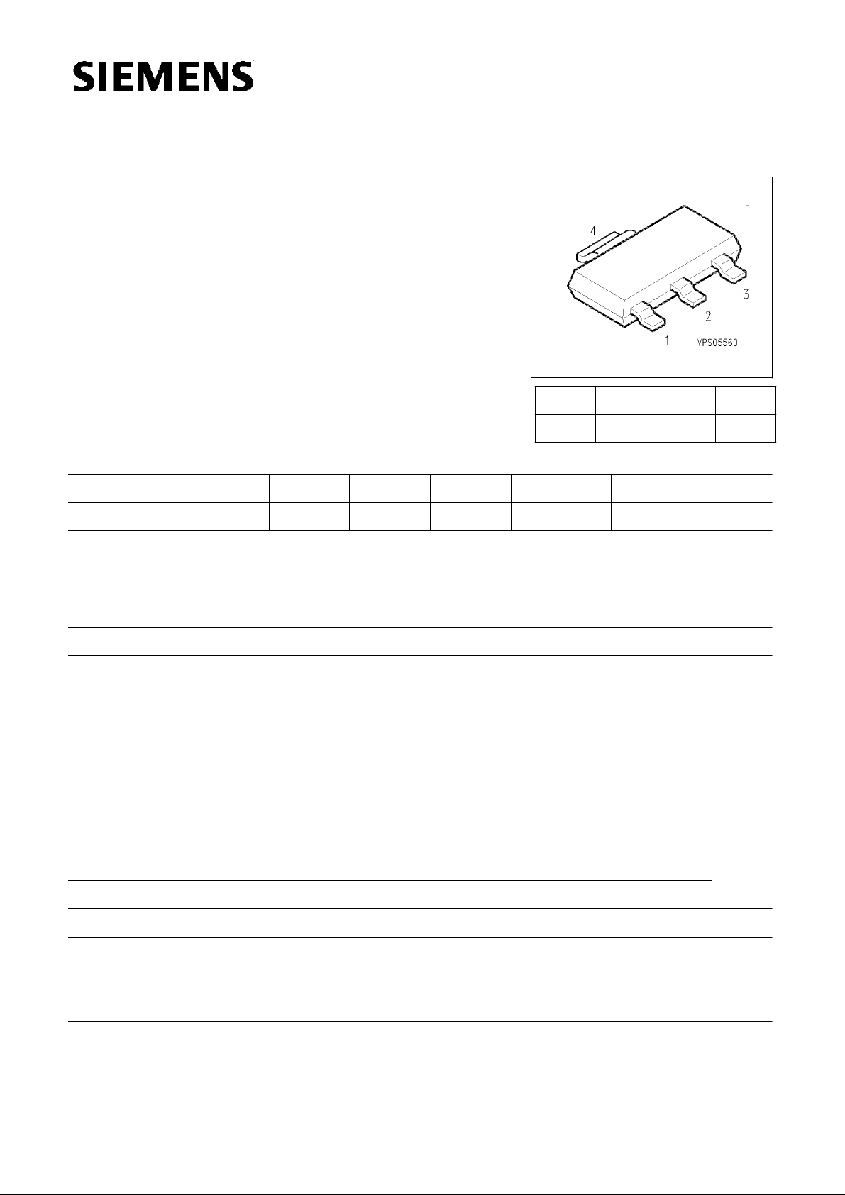
Pin 1 Pin 2 Pin 3 Pin 4
G D S D
Package Marking Ordering Code
SOT-223 Q67000-S4001
Maximum Ratings
Parameter Symbol Values Unit
Continuous drain current
T
= 25 °C
A
T
= 100 °C
A
DC drain current, pulsed
T
= 25 °C
A
Avalanche energy, single pulse
I
= 2.9 A, VDD = 25 V, RGS = 25
D
L = 14.3 mH, T
= 25 °C
j
Avalanche energy, periodic limited by T
Avalanche current, repetitive,limited by T
Ω
j(max)
j(max)
Reverse diode dv/dt
I
= 2.9 A, VDS = 40 V, di/dt = 200 A/µs
S
T
= 150 °C
jmax
Gate source voltage V
Power dissipation
T
= 25 °C
A
I
D
I
Dpuls
E
AS
E
AR
I
AR
dv/dt
GS
P
tot
2.9
1.85
11.6
60
0.18
2.9 A
6
±
20 V
1.8
A
mJ
KV/µs
W
Semiconductor Group 1 29/01/1998
BSP 320 S
Maximum Ratings
Parameter Symbol Values Unit
Chip or operating temperature T
Storage temperature T
Thermal resistance, chip to ambient air
Thermal resistance, junction-soldering point
1)
1)
R
R
j
stg
thJA
thJS
-55 ... + 150 °C
-55 ... + 150
≤
70 K/W
17
IEC climatic category, DIN IEC 68-1 55 / 150 / 56
1) Transistor on epoxy pcb 40 mm x 40 mm x 1,5 mm with 6 cm2 copper area for drain connection
*) MIL STD 883, Method 3015, Class 2
Electrical Characteristics,
at Tj = 25°C, unless otherwise specified
Parameter Symbol Values Unit
min. typ. max.
Static Characteristics
Drain- source breakdown voltage
V
= 0 V, ID = 0.25 mA, Tj = 25 °C
GS
Gate threshold voltage
V
GS=VDS, ID
= 20 µA
Zero gate voltage drain current
V
= 60 V, VGS = 0 V, Tj = -40 °C
DS
V
= 60 V, VGS = 0 V, Tj = 25 °C
DS
V
= 60 V, VGS = 0 V, Tj = 125 °C
DS
Gate-source leakage current
V
= 20 V, VDS = 0 V
GS
Drain-Source on-state resistance
V
= 10 V, ID = 2.9 A
GS
V
(BR)DSS
V
GS(th)
I
DSS
I
GSS
R
DS(on)
60 - -
2.1 3 4
-
-
-
-
0.1
-
0.1
1
100
- 10 100
- 0.09 0.12
V
µA
nA
Ω
Semiconductor Group 2 29/01/1998
BSP 320 S
Electrical Characteristics,
at Tj = 25°C, unless otherwise specified
Parameter Symbol Values Unit
min. typ. max.
Dynamic Characteristics
Transconductance
≥
V
2
DS
* ID * RDS(on)max, ID
= 2.9 A
Input capacitance
V
= 0 V, VDS = 25 V, f = 1 MHz
GS
Output capacitance
V
= 0 V, VDS = 25 V, f = 1 MHz
GS
Reverse transfer capacitance
V
= 0 V, VDS = 25 V, f = 1 MHz
GS
Turn-on delay time
V
= 30 V, VGS = 10 V, ID = 2.9 A
DD
= 33
Ω
R
G
Rise time
V
= 30 V, VGS = 10 V, ID = 2.9 A
DD
= 33
Ω
R
G
Turn-off delay time
V
= 30 V, VGS = 10 V, ID = 2.9 A
DD
R
= 33
G
Ω
Fall time
V
= 30 V, VGS = 10 V, ID = 2.9 A
DD
R
= 33
G
Ω
Gate charge at threshold
V
= 40 V, ID = 0.1 A, VGS 0 to 1 V
DD
Gate Charge at 7.0 V
V
= 40 V, ID = 2.9 A, VGS 0 to 7 V
DD
Gate Charge total
V
= 40 V, ID = 2.9 A, VGS 0 to 10 V
DD
Gate plateau voltage
V
= 15 V, ID = 2.9 A
DS
g
fs
C
iss
C
oss
C
rss
t
d(on)
t
r
t
d(off)
t
f
Q
g(th)
Q
g(7)
Q
g(total)
V
(plateau)
S
2.5 - pF
- 275 340
- 90 120
- 50 65
ns
- 11 17
- 25 40
- 25 40
- 35 55
nC
- 0.24 0.3
- 7.4 9.3
- 9.7 12
V
- 4.7 -
Semiconductor Group 3 29/01/1998
 Loading...