

Siemens BPX90F, BPX90 Datasheet
BPX 90
BPX 90 F
Silizium-Fotodiode
Silicon Photodiode
BPX 90
BPX 90 F
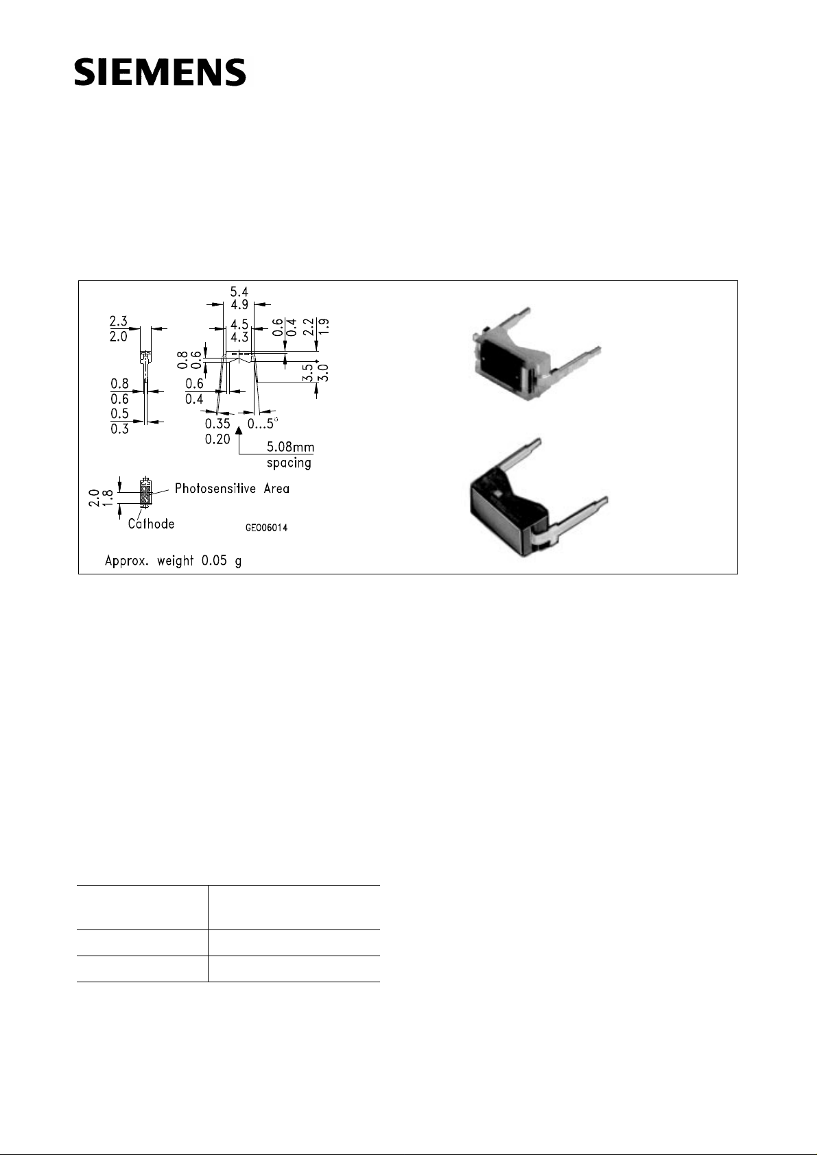
Maße in mm, wenn nicht anders angegeben/Dimensions in mm, unless otherwise specified.
Wesentliche Merkmale
● Speziell geeignet für Anwendungen im
Bereich von 400 nm bis 1100 nm (BPX 90)
und bei 950 nm (BPX 90 F)
● Hohe Fotoempfindlichkeit
● DIL-Plastikbauform mit hoher
Packungsdichte
Anwendungen
● Industrieelektronik
● “Messen/Steuern/Regeln”
Typ
Type
Bestellnummer
Ordering Code
Features
● Especially suitable for applications from
400 nm to 1100 nm (BPX 90) and of 950 nm
(BPX 90 F)
● High photosensitivity
● DIL plastic package with high packing
density
Applications
● Industrial electronics
● For control and drive circuits
BPX 90 Q62702-P47
feof6014 feo06014
BPX 90 F Q62702-P928
Semiconductor Group 1
01.97
Grenzwerte
Maximum Ratings
BPX 90
BPX 90 F
Bezeichnung
Description
Betriebs- und Lagertemperatur
Operating and storage temperature range
Löttemperatur (Lötstelle 2 mm vom
Gehäuse entfernt bei Lötzeit
t ≤ 3 s)
Soldering temperature in 2 mm distance
from case bottom (t ≤ 3 s)
Sperrspannung
Reverse voltage
T
Verlustleistung,
= 25 °C
A
Total power dissipation
Kennwerte
T
= 25 °C
A
Characteristics
Bezeichnung
Description
Symbol
Symbol
T
; T
op
stg
T
S
V
R
P
tot
Symbol
Symbol
Wert
Value
Einheit
Unit
– 40 ... + 80 °C
230 °C
32 V
100 mW
Wert
Value
Einheit
Unit
Fotoempfindlichkeit
Spectral sensitivity
V
= 5 V, Normlicht/standard light A,
R
T = 2856 K,
V
= 5 V, λ = 950 nm, Ee = 1 mW/cm
R
Wellenlänge der max. Fotoempfindlichkeit
Wavelength of max. sensitivity
Spektraler Bereich der Fotoempfindlichkeit
S = 10 % von S
max
Spectral range of sensitivity
S = 10 % of S
max
Bestrahlungsempfindliche Fläche
Radiant sensitive area
Abmessung der bestrahlungsempfindlichen
Fläche
Dimensions of radiant sensitive area
Abstand Chipoberfläche zu Gehäuseoberfläche
Distance chip front to case surface
2
BPX 90 BPX 90 F
S
S
λ
S max
45 (≥ 32)
–
–
26 (≥ 16)
nA/Ix
µA
830 950 nm
λ 400 ... 1150 800 ... 1150 nm
A 5.5 5.5 mm
L × B
× W
L
H
1.75 × 3.15 1.75 × 3.15 mm × mm
0.5 0.5 mm
2
Semiconductor Group 2
 Loading...