

Siemens BPX66, BPX65 Datasheet
BPX 65
BPX 66
Silizium-PIN-Fotodiode
Silicon PIN Photodiode
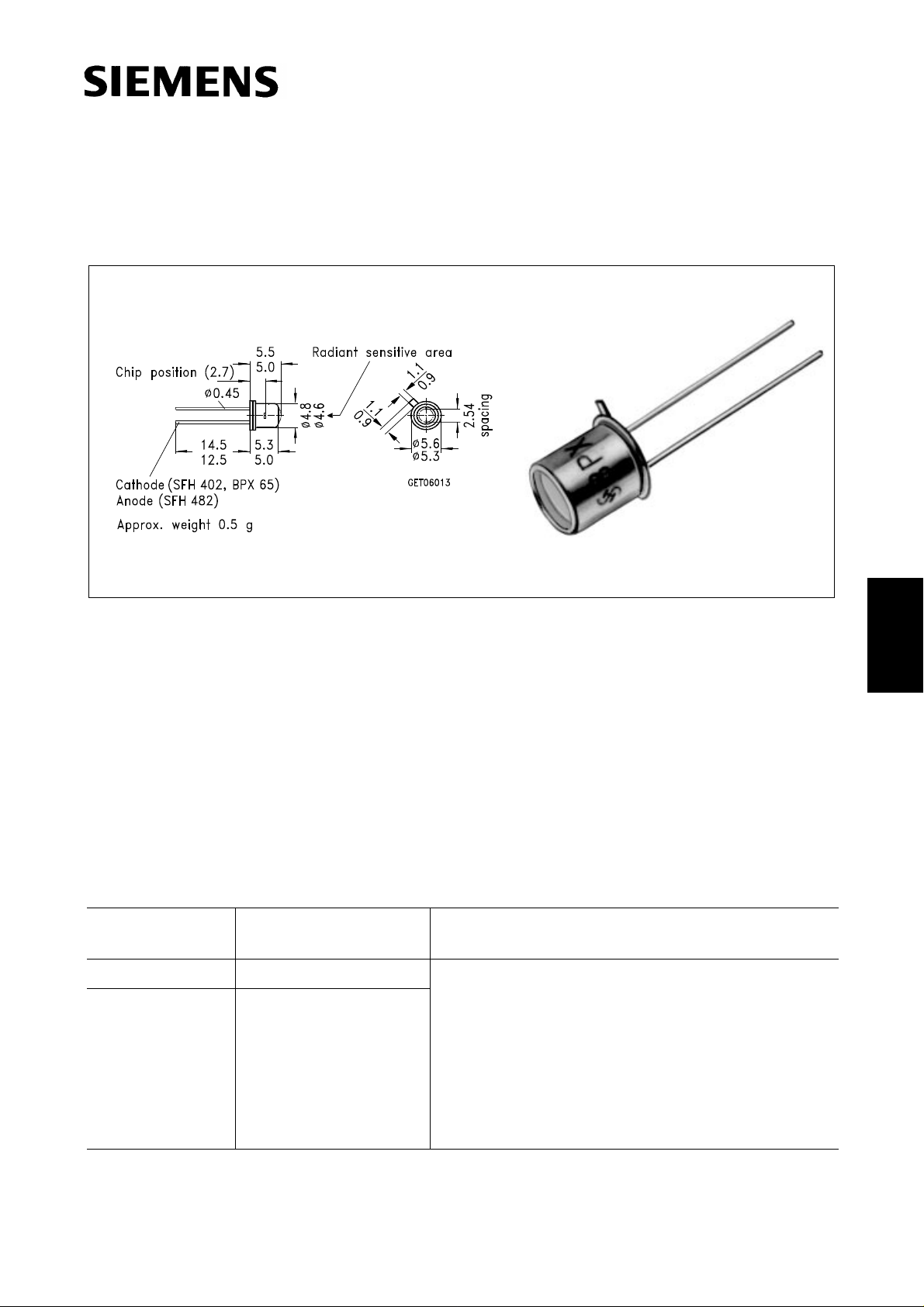
Maβe in mm, wenn nicht anders angegeben/Dimensions in mm, unless otherwise specified.
BPX 65
BPX 66
Wesentliche Merkmale
● Speziell geeignet für Anwendungen im
Bereich von 350 nm bis 1100 nm
● BPX 65: Hohe Fotoempfindlichkeit
● BPX 66: Sperrstromarm (typ. 150 pA)
● Hermetisch dichte Metallbauform (TO-18),
geeignet bis 125oC
1)
Anwendungen
● schneller optischer Empfänger mit groβer
Modulationsbandbreite
Typ
Type
Bestellnummer
Ordering Code
Features
● Especially suitable for applications from
350 nm to 1100 nm
● BPX 65: high photosensitivity
● BPX 66: low reverse current (typ. 150 pA)
● Hermetically sealed metal package (TO-18),
suitable up to 125oC
1)
Applications
● Fast optical sensor of high modulation
bandwidth
Gehäuse
Package
BPX 65 Q62702-P27 18 A3 DIN 41870, planes Glasfenster, hermetisch
BPX 66 Q62702-P80
dichtes Gehäuse, Lötspieβe im 2.54-mm-Raster
2
(
/10”), Anodenkennzeichnung: Nase am Gehäuse-
boden
18 A3 DIN 41870, flat glass lens, hermetically
sealed package, solder tabs 2.54 mm (2/10”) lead
spacing, anode marking: projection at package bottom
1)
Eine Abstimmung der Einsatzbedingungen mit dem Hersteller wird empfohlen bei TA > 85oC
1)
For operating conditions of TA > 85oC please contact us.
Semiconductor Group 342
10.95
Grenzwerte
Maximum Ratings
BPX 65
BPX 66
Bezeichnung
Description
Betriebs- und Lagertemperatur
Symbol
Symbol
T
; T
op
stg
Operating and storage temperature range
Löttemperatur (Lötstelle 2 mm vom
T
S
Gehäuse entfernt bei Lötzeit t ≤ 3s)
Soldering temperature in 2 mm distance
from case bottom (t ≤ 3s)
Sperrspannung
V
R
Reverse voltage
Verlustleistung, T
= 25oC
A
P
tot
Total power dissipation
Kennwerte (T
= 25oC, Normlicht A, T = 2856 K)
A
Characteristics (TA = 25oC, standard light A, T = 2856 K)
Bezeichnung
Description
Symbol
Symbol
Wert
Value
–40 ... +80
230
Einheit
Unit
o
C
o
C
50 V
250 mW
Wert
Value
Einheit
Unit
Fotoempfindlichkeit, V
= 5 V
R
Spectral sensitivity
Wellenlänge der max. Fotoempfindlichkeit
Wavelength of max. sensitivity
Spektraler Bereich der Fotoempfindlichkeit
S = 10% von S
max
Spectral range of sensitivity
S = 10% of S
max
Bestrahlungsempfindliche Fläche
Radiant sensitive area
Abmessung der bestrahlungsempfindlichen
Fläche
Dimensions of radiant sensitive area
Abstand Chipoberfläche zu Gehäuseoberfläche
Distance chip front to case surface
Halbwinkel
Half angle
S 10 (≥ 5.5) nA/Ix
λ
S max
850 nm
λ 350 ... 1100 nm
A 1.00 mm
L x B
1x1 mm
L x W
H 2.25 ... 2.55 mm
ϕ±40 Grad
deg.
2
Semiconductor Group 343
 Loading...