

Siemens BGA420 Datasheet
BGA 420
Semiconductor Group
Jul-13-19981
in SIEGET 25-Technologie
Si-MMIC-Amplifie
r
Preliminary data
• Cascadable 50 Ω-gain block
• Unconditionally stable
• Gain |
S
21
|2 = 13 dB at 1.8 GHz
IP
3out
= +9 dBm at 1.8 GHz
(
V
D
= 3 V,
I
D
= typ. 6.4 mA)
• Noise figure
NF
= 2.2 dB at 1.8 GHz
• Reverse isolation > 28 dB and
return loss
IN
/
OUT
> 12 dB at 1.8 GHz
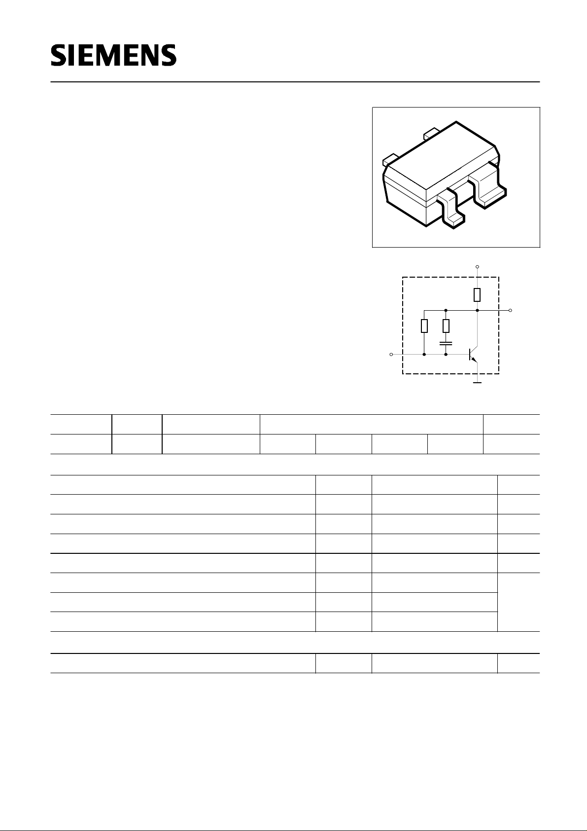
VPS05605
4
2
1
3
EHA07385
D
V
4
2
1
IN
OUT
3
GND
Circuit Diagram
ESD: Electrostatic discharge sensitive device, observe handling precaution!
Type Marking Ordering Code Pin Configuration Package
BGA 420 BLs Q62702-G0057 1, IN 2, GND 3, OUT 4, VD SOT-343
Maximum Ratings
Parameter
Symbol Value Unit
Device current
I
D
15 mA
Device voltage
V
D
V6
Total power dissipation, TS ≤ tbd °C
P
tot
90 mW
R
F
input power
P
RFin
0 dBm
Junction temperature
T
j
150 °C
Ambient temperature
T
A
-65 ...+150
Storage temperature
T
stg
-65 ...+150
Thermal Resistance
≤ tbd
Junction - soldering point
1)
R
thJS
K/W
1)
T
S
is measured on the emitter (GND) lead at the soldering point to the pcb
Semiconductor Group 1 1998-11-01
BGA 420
Semiconductor Group
Jul-13-19982
Electrical Characteristics at
T
A
= 25 °C, unless otherwise specified.
Parameter
ValuesSymbol Unit
typ.min. max.
AC characteristics
6.75.4
I
D
8Device current mA
19
17
13
-
-
-
|
S
21
|
2
17
15
11
Insertion power gain
f
= 0.1 GHz
f
= 1 GHz
f
= 1.8 GHz
dB
28 -
S12
25
Reverse isolation
f
= 1.8 GHz
1.9
2
2.2
Noise figure
f
= 0.1 GHz
f
= 1 GHz
f
= 1.8 GHz
2.2
2.3
2.5
NF
-
-
9
IP
3out
7.5
Intercept point at the output
f
= 1 GHz
- dBm
-1 -
P
-1dB
-2.5
1dB compression point
f
= 1 GHz
Return loss input
f
= 1.8 GHz
8 11 dB-
RL
in
Return loss output
f
= 1.8 GHz
RL
out
12 16 -
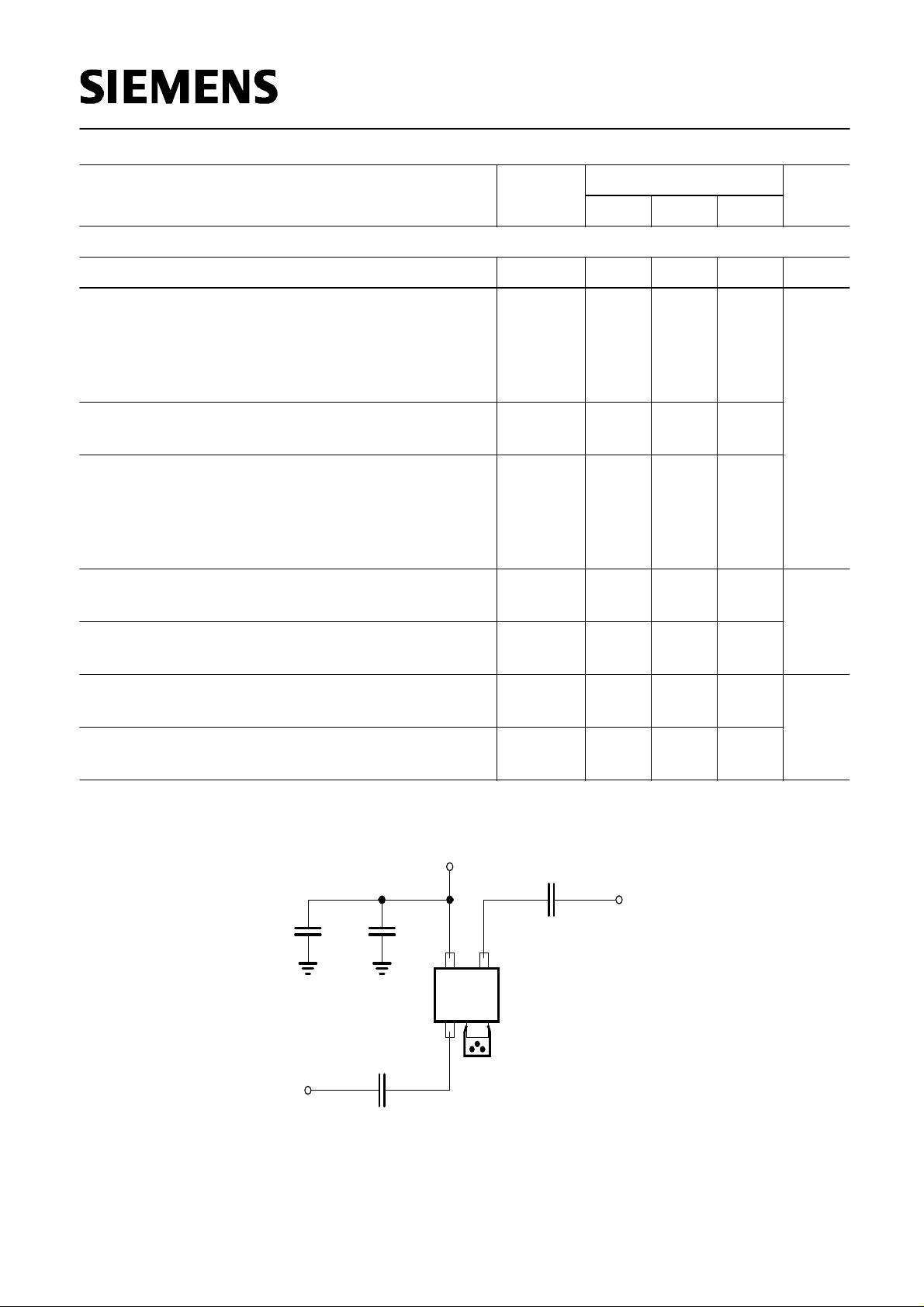
Typical biasing configuration
EHA07386
100 pF
RF IN
100 pF
GND
RF OUT
10 nF100 pF
+
3
12
4
D
V
BGA 420
Note: 1) Large-value capacitors should be connected from pin 4 to ground right at the device
to provide a low impedance path!
2) The use of plated through holes right at pin 2 is essential for pc-board-applications. Thin
boards are recommended to minimize the parasitic inductance to ground!
Semiconductor Group 2 1998-11-01
 Loading...