

Siemens BGA318 Datasheet
BGA 318
Semiconductor Group
Sep-04-19981
Silicon Bipolar MMIC-Amplifier
Preliminary data
• Cascadable 50 Ω-gain block
• 16 dB typical gain at 1.0 GHz
• 12 dBm typical
P
-1dB
at 1.0 GHz
• 3 dB-bandwidth: DC to 1.2 GHz
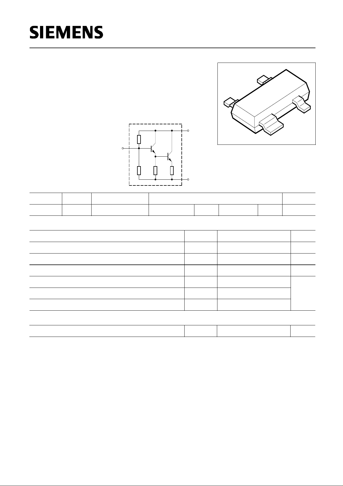
VPS05178
2
1
3
4
EHA07312
3
1
2, 4
RF IN
RF OUT/Bias
GND
Circuit Diagram
Type Marking Ordering Code Pin Configuration Package
BGA 318 BNs Q62702-G0043 1 RFout/bias 2 GND 3 RFinput 4 GND SOT-143
Maximum Ratings
Parameter
ValueSymbol Unit
Device current
I
D
mA60
Total power dissipation,
T
S
≤ 99 °C
250
P
tot
mW
R
F
input power
dBm5
P
RFin
T
j
Junction temperature 150 °C
Ambient temperature
T
A
-65 ...+150
Storage temperature
T
stg
-65 ...+150
Thermal Resistance
Junction - soldering point
1)
R
thJS
≤ 205
K/W
1)
T
S
is measured on the collector lead at the soldering point to the pcb
Semiconductor Group 1 1998-11-01
BGA 318
Semiconductor Group
Sep-04-19982
Electrical Characteristics at
T
A
= 25 °C, unless otherwise specified.
Parameter
ValuesSymbol Unit
max.typ.min.
AC characteristics (
V
D
= 4.7 V,
Z
o
= 50 Ω)
dB
18
16
12
-
-
-
-
-
-
|
S
21
|
2
Insertion power gain
f
= 0.1 GHz
f
= 1 GHz
f
= 1.8 GHz
Insertion point gain flatness
f
= 0.1 GHz to 0.6 GHz
-
∆ |
S
21
|
2
-+-0.7
Noise figure
f
= 0.1 GHz
f
= 1 GHz
f
= 2 GHz
NF
3.5
4
5
-
-
-
-
-
-
1dB compression point
f
= 1 GHz
P
-1dB
- dBm-12
Return loss input
f
= 0.1 GHz to 2 GHz
RL
in
- 14 - dB
Return loss output
f = 0.1 GHz to 3 GHz
RL
out
- 10 -
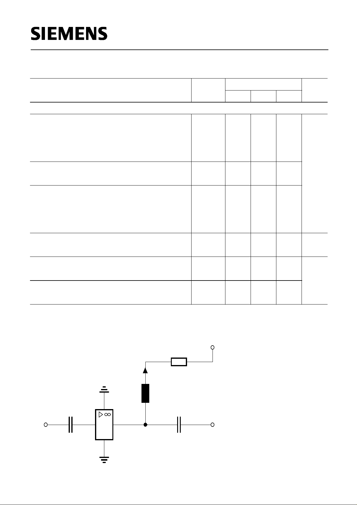
Typical biasing configuration
EHA07313
D
V
RFC (optional)
IN
C
Block Block
C
OUT
Ι
D
Bias
R
min.
CC
V
=7 V
13
2
4
R
Bias
=
V
CC
-
V
D
/
I
D
VD
= 4.7V
Semiconductor Group 2 1998-11-01
 Loading...