

Semiconductor Group 1
PNP Silicon AF Transistors BCW 61
BCX 71
5.91
Type Ordering Code
(tape and reel)
Marking
Package
1)
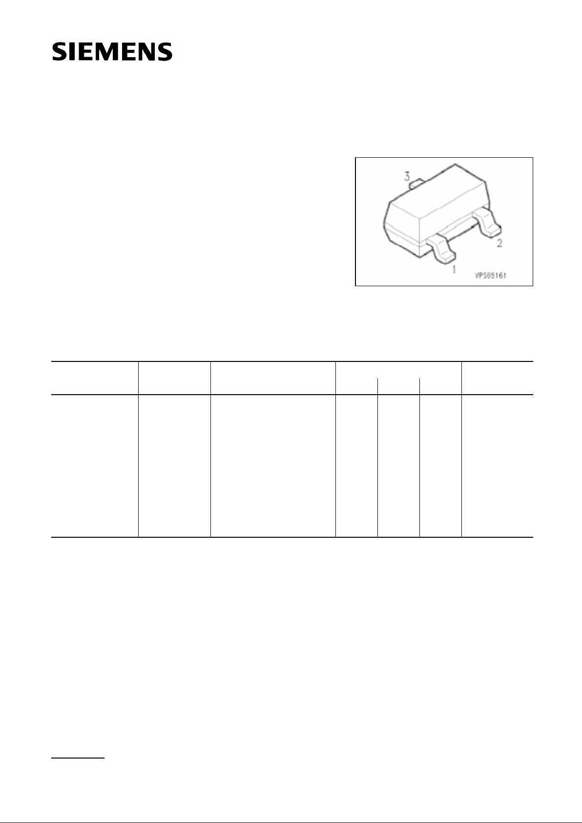
Pin Configuration
BCW 61 A
BCW 61 B
BCW 61 C
BCW 61 D
BCW 61 FF
BCW 61 FN
BCX 71G
BCX 71H
BCX 71J
BCX 71 K
Q62702-C452
Q62702-C1585
Q62702-C1478
Q62702-C1556
Q62702-C1890
Q62702-C1891
Q62702-C1482
Q62702-C1586
Q62702-C1554
Q62702-C1654
BAs
BBs
BCs
BDs
BFs
BNs
BGs
BHs
BJs
BKs
SOT-23
B E C
1 2 3
1)
For detailed information see chapter Package Outlines.
● For AF input stages and driver applications
● High current gain
● Low collector-emitter saturation voltage
● Low noise between 30 Hz and 15 kHz
● Complementary types: BCW 60, BCX 70 (NPN)
BCW 61
BCX 71
Semiconductor Group 2
Maximum Ratings
Parameter Symbol Values Unit
Collector-emitter voltage V
CE0 V
Peak collector current ICM
Collector current IC mA
Junction temperature Tj ˚C
Total power dissipation, T
S = 71 ˚C Ptot mW
Storage temperature range T
stg
Collector-base voltage VCB0
Thermal Resistance
32
100
200
330
150
– 65 … + 150
Emitter-base voltage V
EB0
Peak base current IBM 200
32 45
3232 45
BCW 61
FF
BCW 61 BCX 71
5
Junction - ambient
1)
Rth JA K/W
Junction - soldering point R
th JS
≤ 310
≤ 240
1)
Package mounted on epoxy pcb 40 mm × 40 mm × 1.5 mm/6 cm2 Cu.
BCW 61
BCX 71
Semiconductor Group 3
Electrical Characteristics
at T
A = 25 ˚C, unless otherwise specified.
VCollector-emitter breakdown voltage
I
C = 10 mA BCW 61, BCW 61 FF
BCX 71
V
(BR)CE0
32
45
–
–
–
–
nA
nA
µA
µA
Collector cutoff current
VCB = 32 V BCW 61, BCW 61 FF
V
CB = 45 V BCX 71
V
CB = 32 V, TA = 150 ˚C BCW 61, BCW 61 FF
V
CB = 45 V, TA = 150 ˚C BCX 71
I
CB0
–
–
–
–
–
–
–
–
20
20
20
20
UnitValuesParameter Symbol
min. typ. max.
DC characteristics
Collector-base breakdown voltage
I
C = 10 µA BCW 61, BCW 61 FF
BCX 71
V
(BR)CB0
32
45
–
–
–
–
Emitter-base breakdown voltage
I
E = 1 µA
V
(BR)EB0 5––
–
DC current gain
1)
I
C = 10 µA, VCE = 5 V
BCW 61 A, BCX 71 G
BCW 61 B, BCX 71 H
BCW 61 FF, BCW 61 C, BCX 71 J
BCW 61 FN, BCW 61 D, BCX 71 K
I
C = 2 mA, VCE = 5 V
BCW 61 A, BCX 71 G
BCW 61 B, BCX 71 H
BCW 61 FF, BCW 61 C, BCX 71 J
BCW 61 FN, BCW 61 D, BCX 71 K
I
C = 50 mA, VCE = 1 V
BCW 61 A, BCX 71 G
BCW 61 B, BCX 71 H
BCW 61 FF, BCW 61 C, BCX 71 J
BCW 61 FN, BCW 61 D, BCX 71 K
h
FE
20
30
40
100
120
180
250
380
60
80
100
110
140
200
300
460
170
250
350
500
–
–
–
–
–
–
–
–
220
310
460
630
–
–
–
–
nAEmitter cutoff current
V
EB = 4 V
I
EB0 ––20
1)
Pulse test: t ≤ 300 µs, D ≤ 2%.

BCW 61
BCX 71
Semiconductor Group 4
Electrical Characteristics
at T
A = 25 ˚C, unless otherwise specified.
UnitValuesParameter Symbol
min. typ. max.
V
Collector-emitter saturation voltage
1)
I
C = 10 mA, IB = 0.25 mA
I
C = 50 mA, IB = 1.25 mA
V
CEsat
–
–
0.12
0.20
0.25
0.55
Base-emitter saturation voltage
1)
I
C = 10 mA, IB = 0.25 mA
I
C = 50 mA, IB = 1.25 mA
V
BEsat
–
–
0.70
0.83
0.85
1.05
Base-emitter voltage
1)
I
C = 10 µA, VCE = 5 V
I
C = 2 mA, VCE = 5 V
I
C = 50 mA, VCE = 1 V
V
BE (on)
–
0.55
–
0.52
0.65
0.78
–
0.75
–
DC characteristics
MHzTransition frequency
I
C = 20 mA, VCE = 5 V, f = 100 MHz
f
T – 250 –
AC characteristics
pFOutput capacitance
V
CB = 10 V, f = 1 MHz
C
obo –3–
Input capacitance
V
CB = 0.5 V, f = 1 MHz
C
ibo –8–
kΩShort-circuit input impedance
I
C = 2 mA, VCE = 5 V, f = 1 kHz
BCW 61 A, BCX 71 G
BCW 61 B, BCX 71 H
BCW 61 FF, BCW 61 C, BCX 71 J
BCW 61 FN, BCW 61 D, BCX 71 K
h
11e
–
–
–
–
2.7
3.6
4.5
7.5
–
–
–
–
10
–4
Open-circuit reverse voltage transfer ratio
I
C = 2 mA, VCE = 5 V, f = 1 kHz
BCW 61 A, BCX 71 G
BCW 61 B, BCX 71 H
BCW 61 FF, BCW 61 C, BCX 71 J
BCW 61 FN, BCW 61 D, BCX 71 K
h
12e
–
–
–
1.5
2.0
2.0
3.0
–
–
–
1)
Pulse test: t ≤ 300 µs, D ≤ 2%.

BCW 61
BCX 71
Semiconductor Group 5
Electrical Characteristics
at T
A = 25 ˚C, unless otherwise specified.
dBNoise figure
I
C = 0.2 mA, VCE = 5 V, RS = 2 kΩ
f = 1 kHz,
∆f = 200 Hz
BCW 61 A to BCX 71 K
BCW 61 FF, BCW 61 FN
F
–
–
2
1
–
2
UnitValuesParameter Symbol
min. typ. max.
AC characteristics
–Short-circuit forward current transfer ratio
I
C = 2 mA, VCE = 5 V, f = 1 kHz
BCW 61 A, BCX 71 G
BCW 61 B, BCX 71 H
BCW 61 FF, BCW 61 C, BCX 71 J
BCW 61 FN, BCW 61 D, BCX 71 K
h
21e
–
–
–
–
200
260
330
520
–
–
–
–
µsOpen-circuit output admittance
I
C = 2 mA, VCE = 5 V, f = 1 kHz
BCW 61 A, BCX 71 G
BCW 61 B, BCX 71 H
BCW 61 FF, BCW 61 C, BCX 71 J
BCW 61 FN, BCW 61 D, BCX 71 K
h
22e
–
–
–
–
18
24
30
50
–
–
–
–
µVEquivalent noise voltage
I
C = 0.2 mA, VCE = 5 V, RS = 2 kΩ
f = 10 Hz … 50 Hz
BCW 61 FF, BCW 61 FN
V
n – – 0.11

BCW 61
BCX 71
Semiconductor Group 6
Total power dissipation Ptot = f (TA*; TS)
* Package mounted on epoxy
Permissible pulse load P
tot max/Ptot DC = f (tp)
Collector-base capacitance CCB0 = f (VCB0)
Emitter-base capacitance C
EB0 = f (VEB0)
Transition frequency f
T = f (IC)
V
CE = 5 V

BCW 61
BCX 71
Semiconductor Group 7
Base-emitter saturation voltage
I
C = f (VBEsat)
h
FE = 40
Collector current IC = f (VBE)
V
CE = 5 V
Collector-emitter saturation voltage
I
C = f (VCEsat)
h
FE = 40
DC current gain hFE = f (IC)
V
CE = 5 V

BCW 61
BCX 71
Semiconductor Group 8
Collector cutoff current ICB0 = f (TA)
h parameter h
e = f (VCE)
I
C = 2 mA
h parameter he = f (IC)
V
CE = 5 V
Noise figure F = f (V
CE)
I
C = 0.2 mA, RS = 2 kΩ, f = 1 kHz

BCW 61
BCX 71
Semiconductor Group 9
Noise figure F = f (f)
I
C = 0.2 mA, RS = 2 kΩ,VCE = 5 V
Noise figure F = f (I
C)
V
CE = 5 V, f = 1 kHz
Noise figure F = f (IC)
V
CE = 5 V, f = 120 Hz
Noise figure F = f (I
C)
V
CE = 5 V, f = 10 kHz
 Loading...