

Siemens BC368 Datasheet
NPN Silicon AF Transistor BC 368
● High current gain
● High collector current
● Low collector-emitter saturation voltage
● Complementary type: BC 369 (PNP)
2
3
1
Type Ordering CodeMarking
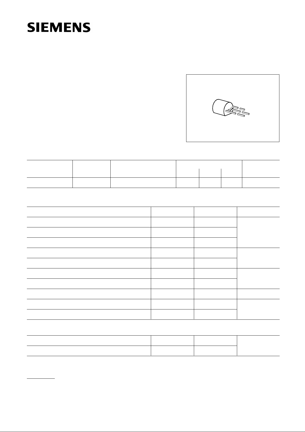
Pin Configuration
Package
1 2 3
BC 368 C62702-C747– TO-92
E C B
Maximum Ratings
Parameter Symbol Values Unit
Collector-emitter voltage V
CE0 20 V
Collector-base voltage VCB0 25
Emitter-base voltage V
Collector current I
EB0 5
C 1A
Peak collector current ICM 2
Base current I
B 100 mA
Peak base current IBM 200
Total power dissipation, T
C = 90 ˚C
2)
Ptot 0.8 (1) W
Junction temperature Tj 150 ˚C
1)
Storage temperature range T
stg – 65 … + 150
Thermal Resistance
Junction - ambient
Junction - case
1)
For detailed information see chapter Package Outlines.
2)
If transistors with max. 4 mm lead length are fixed on PCBs with a min. 10 mm × 10 mm large copper area for
the collector terminal, RthJA = 125 K/W and thus Ptot max = 1 W at TA = 25 ˚C.
3)
Mounted on Al heat sink 15 mm × 25 mm × 0.5 mm.
2)
3)
Semiconductor Group 1
Rth JA ≤ 156 K/W
Rth JC ≤ 75
5.91
Electrical Characteristics
I
I
I
I
I
I
I
I
I
I
A = 25 ˚C, unless otherwise specified.
at T
DC characteristics
BC 368
UnitValuesParameter Symbol
min. typ. max.
V
(BR)CE0 20 – –
C = 30 mA
Collector-base breakdown voltage
C = 10 µA
Emitter-base breakdown voltage
E = 1 µA
Collector cutoff current
CB = 25 V
V
CB = 25 V, TA = 150 ˚C
V
EB = 5 V
V
V
(BR)CB0 25 – –
V
(BR)EB0 5––
CB0
I
–
–
I
EB0 – – 100
–
–
100
10
hFE
C = 5 mA; VCE = 10 V
C = 500 mA; VCE = 1 V
C = 1 A; VCE = 1 V
Collector-emitter saturation voltage
C = 1 A; IB = 100 mA
Base-emitter voltage
C = 5 mA; VCE = 10 V
C = 1 A; VCE = 1 V
1)
1)
1)
1)
VCEsat – – 0.5
V
BE
50
85
60
–
–
–
160
–
0.6
–
–
375
–
–
1
VCollector-emitter breakdown voltage
nA
µA
nAEmitter cutoff current
–DC current gain
V
AC characteristics
C = 100 mA, VCE = 5 V, f = 20 MHz
f
T – 100 –
MHzTransition frequency
1)
Pulse test: t ≤ 300 µs, D ≤ 2%.
Semiconductor Group 2
 Loading...