

Siemens BAR63-02W Datasheet
BAR 63-02W
Semiconductor Group
Sep-07-19981
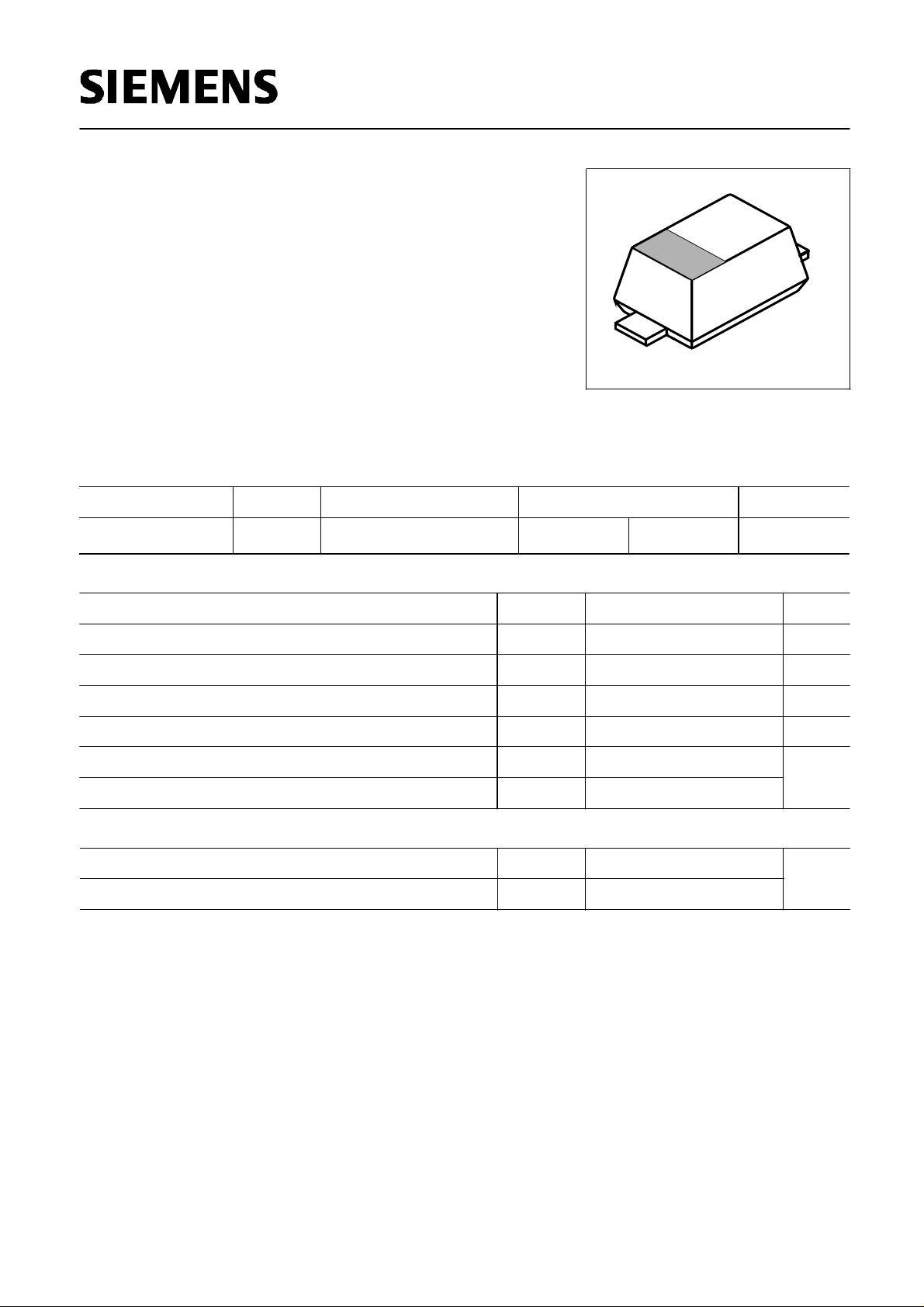
Silicon PIN Diode
• PIN diode for high speed switching
of RF signals
• Low forward resistance, small capacitance
small inductance
• Very low capacitance
• For frequencies up to 3 GHz
1
VES05991
2
Type Marking Ordering Code Pin Configuration Package
BAR 63-02W G Q62702-A1211 1 = C 2 = A SCD-80
Maximum Ratings
Parameter ValueSymbol Unit
Diode reverse voltage V50
V
R
Forward current 100
I
F
mA
Total power dissipation,
T
S
= 115 °C
P
tot
mW250
Junction temperature
T
j
°C150
Operating temperature range
T
op
-55 ...+150 °C
Storage temperature
T
st
g
-55 ...+150
Thermal Resistance
Junction - ambient
1)
R
thJA
≤ 220
K/W
Junction - soldering point
R
thJS
≤ 140
1) Package mounted on alumina 15mm x 16.7mm x 0.7mm
Semiconductor Group 1 1998-11-01
BAR 63-02W
Semiconductor Group
Sep-07-19982
Electrical Characteristics at
T
A
= 25 =C, unless otherwise specified.
Parameter Symbol UnitValues
min. typ. max.
DC characteristics
-
V
(BR)
50Breakdown voltage
I
(BR)
= 5 µA
- V
Reverse current
V
R
= 35 V
µA
I
R
- 10-
Forward voltage
I
F
= 100 mA
V
F
- 0.95 1.2 V
AC characteristics
Diode capacitance
V
R
= 0 V, f = 100 MHz
V
R
= 5 V, f = 1 MHz
C
T
-
-
0.3
0.21
-
0.3
pF
Case capacitance
f
= 1 MHz
C
C
- 0.09 -
Forward resistance
I
F
= 5 mA, f = 100 MHz
I
F
= 10 mA, f = 100 MHz
r
f
-
-
1.2
1
2
-
Ω
Charge carrier life time
I
F
= 10 mA,
I
R
= 6 mA,
I
R
= 3 mA
τ
rr
- 75 - µs
Series inductance
L
s
- 0.6 - nH
Semiconductor Group 2 1998-11-01
 Loading...