

Page 1
Service Manual
UC1
/ UC1L Body-Pack
Characteristics
General
The Shure UC1/UC1L Body-Pack Transmitter is microprocessorcontrolled, operating in the 774 – 862 MHz frequency range. The UC1/
UC1L is used in mid-level installed sound, rental, and concert sound
applications. Six frequency range variations are available.
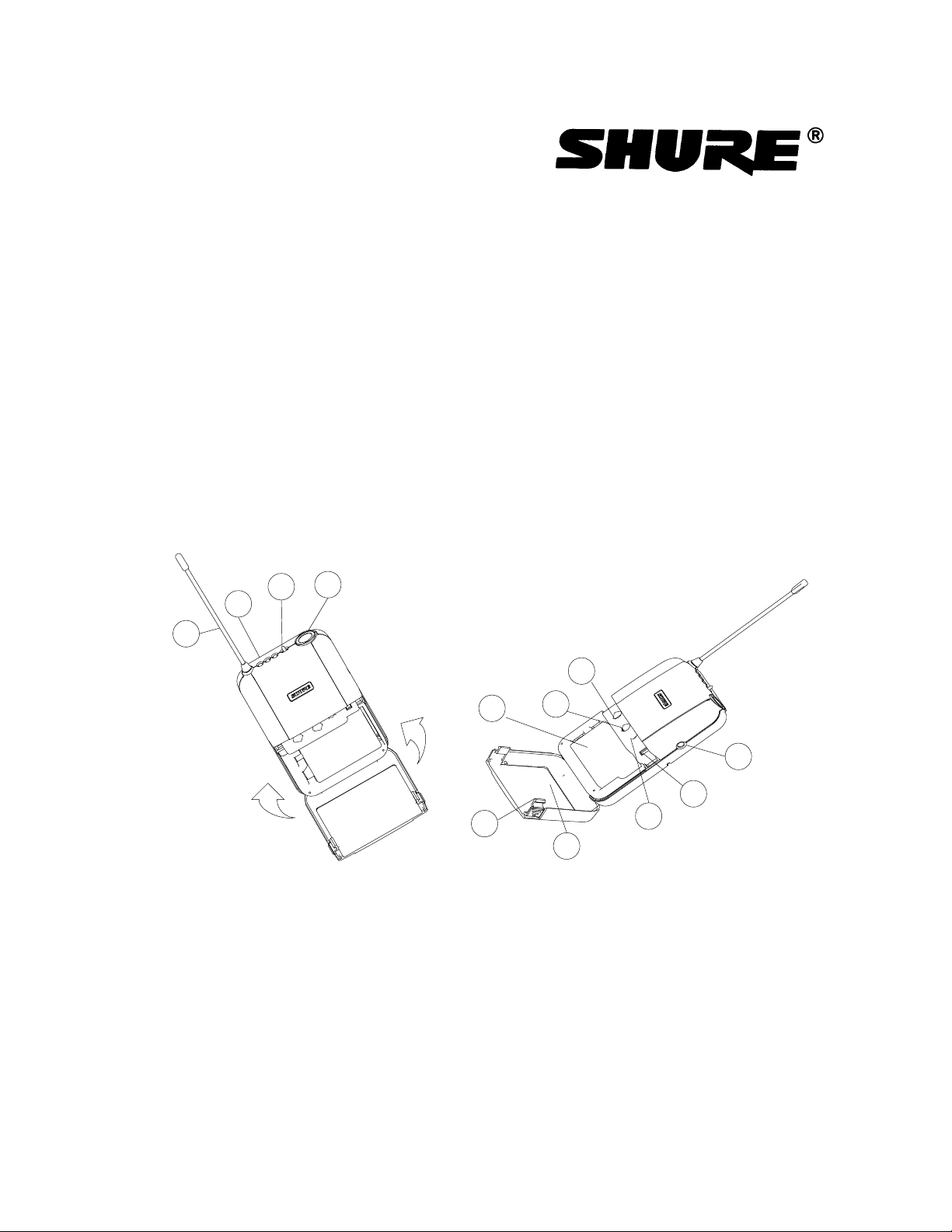
Controls and Connectors
4
3
2
1
UHF Transmitter
8
10
9
5
6
11
12
1. Antenna
2. Power/Battery Fuel Gauge LEDs
3. Power ON/OFF Switch
4. Input Connector
5. Rf/Audio Mute Switch Input Connector
6. Input Attenuation Control
Figure 1. UC1 Controls and Connectors
Service Note:
performed by a Factory-Authorized Service Center or that the
product be returned directly to Shure Brothers Inc.
E1998, Shure Brothers Inc. Printed in U.S.A.
25A1043 (RI)
Shure recommends that all service procedures be
7. Audio Gain Control
8. Group Rotary Switch
9. Channel Rotary Switch
10. Battery Compartment
11. Battery Cover Release Tabs
12. Battery Compartment Cover
7
Page 2
Shure UC1 Body-Pack UHF Transmitter
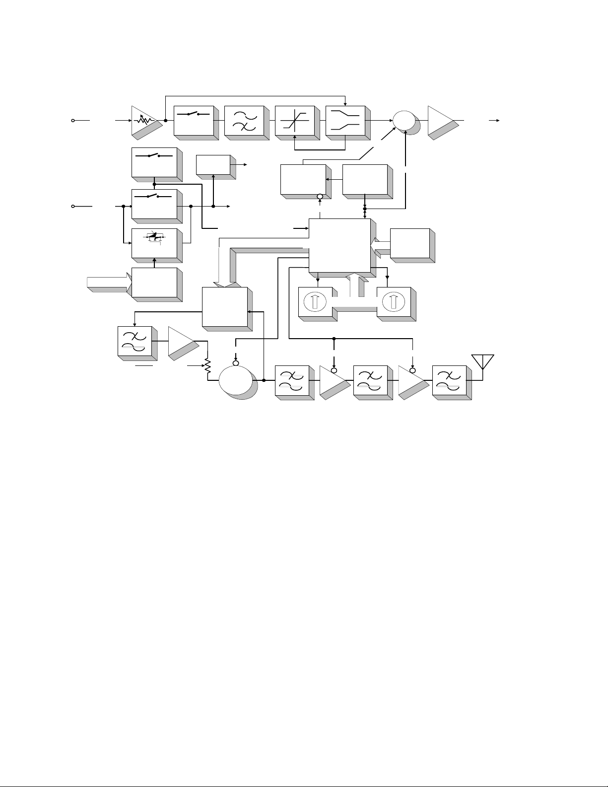
Circuit Description
LIMITER CONTROL INPUT
MIC. /
INSTR.
FROM
BATT.
REMOTE
MUTE
ON / OFF
SWITCH
FET
BYPASS
MIC. /
INSTR.
+5V
REG.
OFF / MUTE DETECT
+5v
UNREG. PWR.
PLL CONTROL
LIMITER
CONTROL OUTPUT
TONE KEY
CIRCUIT
TONE CONTROL
MCU
TONE KEY
BATTERY
MGMT.
& FUEL
GAUGE
Σ
CALL ID
EEPROM
(MEM)
AUDIO
OUT
CONTROL
PWR.
HOLD
CIRCUIT
AUDIO IN
Audio Section
SYNTH.
GROUP CHANNEL
RF POWER
VCO
RF MUTE RF MUTE
Figure 2. UC1 Circuit Block Diagram
Domestic Models
The audio signal enters the audio board at J204, pin 1. The signal
then enters a switchable 20 dB pad made up of SW203, R203, R204,
C204, and C206. The back-to-back diodes, U206, are used to keep
the op-amp from snapping to the rail and reverse-phasing when the
maximum input voltage range is exceeded.
Service Procedures
The signal is ac-coupled through C205 into a 40 dB (30 dB for
J frequencies) user-adjustable gain stage around amplifier U2. This
gain stage is externally accessible to the user. Due to its topology, it is
a unique stage because it is non-inverting and allows for a gain less than
unity. Resistors R205 and R207 set up a half-supply bias, and R206 sets
the ac input impedance.
The amplified audio signal then passes through a pre-emphasis
network before entering the compression stage. R221, R222, C215,
and C216 set up two corners for the pre-emphasis network. The preemphasis network feeds the NE575 compander, U203, which utilizes
2 25A1043 (RI)
Page 3

Shure UC1 Body-Pack UHF Transmitter
an external amplifier, U202B. U203 performs a 2:1 logarithmic compression of the audio signal.
Transistors Q201 and Q202, with crystal Y201, form the tone key
oscillator circuit that provides a stable, continuous 32.768 kHz sine
wave. Q204 buffers the tone key signal before it is added to the audio
signal. The tone key signal is used in the receiver to provide audio output only when the tone key signal is present in the transmitted signal.
If the tone key or the transmitter is turned off, the receiver is muted.
Q211 acts as a switch for toggling the tone key ON/OFF. It is con-
trolled from the microprocessor, via the TONEMUTE0 signal. The tone
key signal, along with the processed audio signal, is then fed to a summing amplifier, U201A. After passing through the ac coupling capacitor,
C240, the signal is then fed to the rf module.
The battery meter circuit is comprised of comparator U208 and
LEDs D201, D202, D203, and various resistors. When the battery circuit
is less than 6.5 Vdc, the output of U208, pin 13, changes low, the red
LED illuminates, and the tone-key level increases. The receiver then
utilizes the amplitude of the tone-key to indicate that the transmitter
battery is low.
Rf Section
A 9 Vdc battery provides power to the audio printed circuit board
(pcb) through switch SW202. FET Q217 provides electrical reverse
battery protection. 9 Vdc enters U205, a low-dropout 5 Vdc regulator,
and gives a clean regulated 5 Vdc supply to run the audio circuitry.
ETSI Models
This transmitter uses the same board as the non-ETSI system,
except that it requires a different topology and different parts.
A limiter is inserted between the pre-emphasis and the compressor
to limit the occupied bandwidth. The buffer after the gain stage, U201A,
is now an inverter with pre-emphasis and 20 dB of attenuation.
Previously bypassed, the expander side of U203 is now activated
and used as a limiter. A sample of the audio is taken from the limiter
output (U203, pin 6) and sent to a control circuit which detects signals
from a limiting threshold.
The comparator then sends a control signal to U202, pin 5, which
clamps the signal.
Processed audio enters R149, an internal potentiometer that is
adjusted for 45 kHz deviation (100% modulation for UA, MA, and MB
frequencies), with a –7.2 dBV (0.355 Vrms) 1 kHz tone at the output
of the front audio stage (U201, pin 1). For KK frequencies, R243 is
adjusted for 40 kHz deviation. For JB frequencies, R149 is adjusted for
5 kHz deviation with –63.2 dBV, 1 kHz tone at the input to the transmitter.
25A1043 (RI)
3
Characteristics
Page 4

Shure UC1 Body-Pack UHF Transmitter
The audio is then fed to the tuning voltage pin of the voltage-
controlled oscillator (VCO) and modulates the carrier directly .
Using a phase-locked loop (PLL) frequency synthesized system
eliminates the need for multiplier stages and results in a much higher
degree of spectral purity. The VCO is shielded to prevent external rf
fields from affecting its operation.
Regulated 5 Vdc power is provided to ensure frequency stability with
changes in battery voltage.
The VCO can tune from 782 MHz to 810 MHz with a 1 Vdc to 4 Vdc
tuning voltage range; different VCOs are required for MB and KK frequency models. At the output of the
The output of the VCO is coupled by C134 to the frequency control
pin of the synthesizer, U104, pin 8. The internal circuitry of the synthesizer divides the signal, as necessary, to the desired reference frequency
of 125 kHz. The synthesizer contains a reference oscillator circuit operating from a 4.0 MHz quartz crystal, Y101, that is adjusted by trimmer
C123. The transmitter output frequency is user-selectable in 125 kHz
increments, from 782 MHz to 806 MHz. Frequency range and increment
size vary for each model.
VCO, the rf signal splits into two paths.
Frequency selection is made via microprocessor U101, which interfaces the user by means of the mode/select switches. The output of the
synthesizer is a series of pulses which are integrated by a passive loop
filter, R121, C130, R122, C129, C130, R123, and C132, to produce a
control voltage signal. The control voltage signal is then connected to
VCO through amplifier U106A, which is used to isolate the PLL filter
the
from the audio modulation signals.
The
VCO output is also coupled to an rf power amplifier through a
resistive pad consisting of R127, R128, R129, and R130. The signal is
then low-pass filtered through U107. The signal is coupled through C144.
Transistor Q102 acts as an rf pre-amplifier stage with typically 8 dB
of gain. R131, R132, and R133 provide dc bias to Q102. C145, C146,
C147, C149, C150, and L111 are used to decouple the rf off the emitter
of Q102, Vcc, and +9 Vdc supply voltages.
C152 couples the output of Q102 to low-pass filter U108. The signal
is then low-pass filtered through U108, and then coupled through C157.
Q104 acts as an rf amplifier stage with typically 16 dB of gain. L110,
R136, R137, and R138 provide dc bias to Q102. C160, C161, C162,
C163, C164, C165, and L114 are used to decouple the rf off the emitter
of Q104, Vcc, and +9 Vdc supply voltages.
L115 and C167 match the output of Q104 to low-pass filter U109.
The signal is coupled through C173 to the output antenna, W101.
Characteristics
The transmitter can deliver a maximum of +17 dBm (50 mW) to
the 50Ω antenna. During transmitter power-up and frequency selection,
the rf power is muted by bringing the gate of Q103 and Q105 high. The
RFUNMUTE signal is 5 Vdc. This provides approximately 45 dB rf attenu-
ation until the PLL has locked.
4 25A1043 (RI)
Page 5

Shure UC1 Body-Pack UHF Transmitter
The transmitter is unmuted by bringing the gate low (RFUNMUTE).
During transmitter power OFF conditions, the rf power is first muted by
bringing the base of Q103 and Q105 high. When the rf is muted this
way, the carrier signal of the transmitter is not allowed to drift off
frequency during power
When the external mute switch is closed, the ring and sleeve on the
jack are connected, or the tip and sleeve can be connected, depending
on how the switch is wired.
If the tip is connected to the sleeve, this grounds the IRQ signal
line that is connected to the microprocessor. Then, the 33 kHz tone key
signal is muted (
bringing the base of Q103 and Q104 high (RFMUTE1). Finally, the rf
power is then turned off via the RFOFF1 signal. This is done by reducing
the Vcc line to the VCO and the last rf amps.
TONEMUTE1). The transmitter rf power is muted by
ON or OFF conditions.
If the ring is connected to the sleeve, this grounds the
The TKMUTE1 grounds Q4 at the output of the tone key oscillator circuit.
This mutes the audio signal immediately.
Transmitter Display Board
UHF Body-Pack Transmitter Digital Section
The digital section contains several circuitry blocks.
Microcontroller Section
The microcontroller section consists of a U101 microcontroller. The
rotary switches indicate the UHF frequency group and channel. A 4.000
MHz oscillator provides the operating frequency to the microcontroller.
The oscillator circuit includes C117, C118, and Y102. U103, R106, and
C120 form the reset circuit. U103 is the reset IC that resets the U101
microcontroller if the 5 Vdc normal operating voltage falls below 4.3 Vdc.
R115 and C119 form the power supply filter circuit.
Memory Section
The memory section consists of U102, a non-volatile Electrically
Erasable / Programmable Read Only Memory (EEPROM) that stores the
mapping of compatible groups and channels. The microcontroller serially
communicates with this part via data and clock lines to read the frequency corresponding to the group and channel position. Ability to write to
this memory occurs during factory programming only.
TKMUTE1.
25A1043 (RI)
During normal usage, this memory is used as a look-up table only.
Additional detail about the contents of
ing sections.
R103 and R108 resistors allow the clock and data lines to be driven
independently of the microcontroller port pin states during in-circuit
programming of EEPROM.
5
EEPROM is covered in the follow-
Characteristics
Page 6

Shure UC1 Body-Pack UHF Transmitter
Battery Management Section
The microcontroller provides for low battery shutdown. The shutdown threshold is 1.88 Vdc ± 10%. A voltage lower than the shutdown
threshold on pin 17 of the U101 microcontroller shuts down the transmitter. Resistors R104 and R105 divide down the battery voltage for the
microcontroller. A battery voltage of less than 5.65 Vdc shuts down the
transmitter.
This auto shutdown disables the audio tone key mix, mutes the rf
power output, and power downs the rf output amplifier section. The current draw from a 9 Vdc battery in this state is 45 mA, and the battery fuel
gauge is functional. Turning off the power switch must completely shut
off the transmitter.
The audio circuit description provided the battery fuel gauge circuit
description.
Rotary Switches for Frequency Selection
A 10-position Group switch, S101, and a 16-position Channel switch,
S102, select the transmitter frequency. Both rotary switches share the
same U101 microcontroller port pins, 3 through 6, for a multiplexed
switch read operation.
Pins 7 and 8 of the U101 microcontroller select the individual
switches. Resistors R109 through R112 are the pull-ups for the switch
position read. Diode packs D101 through D104 isolate the switches during a multiplexed read operation.
The multiplexed switch read system does not allow switch change
detection based on interrupts. Also, the switches cannot be constantly
scanned to determine changes, because the scanning frequency being
in audio range is difficult to filter out.
In a steady state, the switch selector common pins are inputs to the
U101 microcontroller pins 7 and 8. Pins 3 through 6 are outputs. In this
state, pins 4, 5, and 6 are held low, while pin 3 is held high. This forces a
logic high level on the switch selector pins if the switches are set on odd
positions. If the switches are set on even positions, the contact on pin 1
is open from the switch common pin, and the pull-down resistors, R114
and R115, force the logic low to pins 7 and 8 of U101.
Any switch change is made by a state toggle from odd to even, or
vice versa. Only this change can be detected and is followed by a multiplexed switch read. In this case, U101 pins 7 and 8 become selectively
grounded outputs to read the selected switch’s state on pins 3 through 6.
A multiplexed switch read is preceded by tone key and rf mutes.
This mutes the audio in the receiver to allow a quiet change to another
frequency.
Characteristics
6 25A1043 (RI)
Page 7

Shure UC1 Body-Pack UHF Transmitter
Power Switch and Remote Mute Switch Interface
When a transmitter is turned off, the PWRDN1 signal goes to logic low
on U101, pin 19. The same signal is also forced low when a remote
mute switch closes the tip contact to the sleeve ground.
The microcontroller treats both of these events in a similar manner.
It immediately disables the tone key, and the power hold circuit automatically kicks in to bypass the power switch. Followed by 500 msec.
of delay, the rf is muted and also turned off.
The power hold circuit is also disabled at this point. If it is the power
off condition, then the transmitter is shut off. Otherwise, it is the remote
mute condition, and the transmitter waits here for unmute to occur.
PWRDN1 is pulled up back to logic high level when unmute occurs.
The rf section repowers and is unmuted, followed by tone key enable
to completely recover from the remote mute condition. When a remote
mute switch closes the ring contact to the sleeve ground, the
signal goes to a logic low that immediately mutes the audio.
TKMUTE1
25A1043 (RI)
7
Characteristics
Page 8

Shure UC1 Body-Pack UHF Transmitter
Notes
Notes
This page intentionally left blank.
8 25A1043 (RI)
Page 9
Shure UC1 Body-Pack UHF Transmitter
Functional Test
Verify operation and reported malfunction, referring to the product
User Guide
operation, troubleshooting, and technical data.
for a description of the unit as well as information on its
Disassembly and Assembly
! CAUTION !
Observe precautions when handling this static-sensitive device.
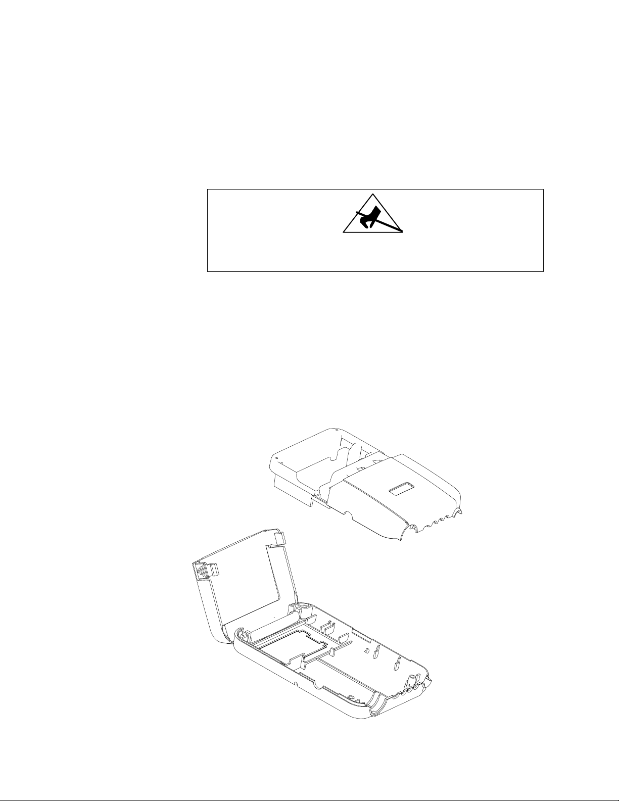
Disassembly
1. Open the battery compartment and remove the battery.
2. Remove the belt clip.
3. With the battery compartment open, remove the four screws
from the back of the case.
4. Lift the top half of the transmitter case away to expose the
printed circuit boards (pcbs).
5. Lift the pcbs out of the transmitter case.
Figure 3. UC1 Disassembly
25A1043 (RI)
9
Functional Test
Page 10

Shure UC1 Body-Pack UHF Transmitter
Reassembly
After completing all repairs and alignment, reassemble the UC1:
1. Place the printed circuit boards back into the case, making sure
the multi-pin connectors on the board mate and the
LEMO
connector is seated correctly.
2. Reassemble the transmitter by performing the disassembly steps
in reverse order.
TINI QG/
Disassembly and Assembly
10 25A1043 (RI)
Page 11

Service Procedures
Measurement Reference
dBu is a measure of
For example, the HP8903 should be labeled dBu instead of dBm
because it is a voltage measurement. These two terms are often used
interchangeably even though they have different meanings.
Audio levels in dBu are marked as dBm on the HP8903.
0 dBV = 2.2 dBu
0 dBu = 0 dBm, assuming the load = 600 Ω
Test Equipment
Most test equipment needed is described in the Shure
Service Equipment Manual
equivalent) is also needed.
Shure UC1 Body-Pack UHF Transmitter
voltage
dB Conversion Chart
, and dBm is a measure of
. The following test equipment (or approved
power
Wireless
.
Equipment Type Model
Audio analyzer *Hewlett-Packard 8903B
Digital multimeter Fluke 87
Frequency counter Hewlett-Packard 53181A
Rf signal generator Hewlett-Packard 8656B
Spectrum analyzer Hewlett-Packard 8590L
Shure UC4 receiver Shure UC4
*Audio levels in dBu are marked as dBm on the HP8903B.
Test Equipment Set-Up
The alignment procedure is sequential and does not change,
unless specified.
1. Use RG58 or any other low-loss, 50 Ω test cables for all
rf connections. For JA, JB frequencies, use an adapter cable.
2. Keep the test cables as short as possible.
Table 1
Test Equipment
Cable PT1843
25A1043 (RI)
3. Include the insertion loss of the cables and the connectors
for all rf measurements.
4. Dc voltages are present at most rf test points. Use dc blocks
to protect the test equipment, if necessary.
11
Service Procedures
Page 12

Shure UC1 Body-Pack UHF Transmitter
Test Set-Up
C123
TP131
C130
TP5
SIDE 1
Q3
MIC1
TP
Q2
D206
TBIAS1
U1
J204
*R144
U108
Q104
L115
*J103
TP107
W101
*R144 and J103 are for JA, JB frequencies only.
J301
TP3
SW202
C220
D203
D202
D201
TP4
Y201
TP106
GND
TP
PAD
C225
C255
AUD1
TP102
TP110
Y103
C223
TP2
TP
GND1
TP239
VCO
C257
C256
TBIAS1
C219
Q4
C240
U501
TP103
U701
C510
C119
CA
TP1
TPA1
TP18
TP9
TP21
TP14
TP10
TP111
TP120
B
D
TP130
R149
TP104
+ 9V
+ 5V
F
GE
H
TP+5
TP13
TP19
TP12
TP6
+ 9V
GREEN
J202
SW203
R7
U205
J201
TP8
Q213
S102
S101
RED
+ 9 Vdc
TPMIC1
C206
Q217
TP108
TP109
TP17
TP16
J203
TP7
TP16
SIDE 2
TP108
TP109
TP7
TP17
L208
C208
C203
STR1
C246
TP8
Q218
J101
D104
L205
TP6
D103D101
D102
TP13
TP19
+ 9V
TP+5
TP12
TP10
Q220
D105
TP111
TP104
+ 5V
U2
TP9
Q215
U106
Q216
U208
+ 9V
TP130
TP5
Q101
C176
U103
TP120
TP1
TPA1
TP18
Q223
Y102
4.000
TP14
TP103
J202
TP2
TP21
TP
Q201
TP239
U203
GND1
Q202
U104
U107
TP102
TP3
U201
AUD1
TP
Y101
4.000
TP110
TP106
U102
TP4
Q204
Q103
TP107
J401
C176
W101
Q222
Q105
U109
Q219
Q221
Q1
B
A
C
D
F
EG
H
PAD
Service Procedures
Figure 4. UC1 Major Test Component Locations
1. Use the PT1843 cable to connect the rf-digital board and the
audio board through the 11-pin board interconnects (J101, J201,
side 2).
2. Apply +9 Vdc across the battery terminals (J202, J203, side 1).
3. Set audio GAIN potentiometer (R7, side 2) to minimum
(full counter-clockwise ).
4. Rf power and tone key level measurements are made by
connecting W101 (rf output) to the spectrum analyzer. Use
the frequency counter to measure frequency. For JA, JB
frequencies, connect J103 (rf output) to the spectrum analyzer
and frequency counter.
5. See Table 2 for frequency settings.
12 25A1043 (RI)
Page 13

Alignment
Shure UC1 Body-Pack UHF Transmitter
Alignment Set-Up
Table 2 lists the group carrier frequencies and
tuning voltages for all the service tests that follow.
Table 2
Group Carrier Frequencies and Tuning Voltages
(in order by carrier frequency)
Group
Group
UA A 4 0 805.500 3.7 45
MB B 1 3 805.500 1.8 15
JA C 0 2 805.500 3.5 5
JB D 4 2 807.500 3.7 5
KK E 5 5 851.125 3.5 15
MC – – – – – –
Group
Code
Switch
(S101)
Channel
Switch
(S102)
Carrier
Frequency
(MHz)
VCO Tuning
Voltage
(TP130)
Deviation
(kHz)
25A1043 (RI)
13
Service Procedures
Page 14

Shure UC1 Body-Pack UHF Transmitter
Frequency
Use this service procedure to correctly align the transmitter’s
operating (output) frequency. C510 tunes the voltage-controlled
oscillator (VCO) to the operating frequency selected, with a 1 – 4 Vdc
tuning range.
C123 adjusts the reference oscillator on the synthesizer.
FREQUENCY COUNTER
SIDE 1
*R144
VCO
C123
C510
U501
TP130
R149
S102
(GREEN)
DC VOLTMETER
+
–
CH 2
CH 1
*R144 and J103 are for JA, JB frequencies only.
*J103
W101
UC1 Transmitter Frequency Counter
Power: ON Operating freq: See Table 2 Connect + : TP130
Operating freq: See Table 2 Connect CH 2: W101 and GND
For JA, JB use
J103 and GND
Figure 5. UC1 Frequency Alignment Test Set-Up
1. Remove the antenna and connect the 50 Ω cable, center
conductor to W101, and shield to GND, as shown in Figure 5.
(For JA, JB frequencies, use J103 and GND.)
2. Connect the BNC cable end to the frequency counter, CH 2.
3. Measure the dc voltage at TP130 (tuning voltage line) and
ground (GND).
GND
S101
(RED)
J202
J201
DC Voltmeter
Connect – : J202 (ground)
Service Procedures
4. Use the pink torey to adjust the VCO trimmer, C510, until the
voltmeter reading equals that shown in Table 2, ± 0.125V..
5. Use the blue torey to adjust the variable capacitor, C123, until
the frequency counter measurement matches the desired
frequency, within ± 1 kHz.
6. Disconnect the test cable from the frequency counter.
7. Use the test set-up and equipment settings in Figure 6 for
the next test, the power output measurement.
14 25A1043 (RI)
Page 15

Power Output Measurement
The output power measurement ensures that the output signal is
strong enough for sufficient range when the system is in use. The output
power measurement also verifies that the output power is not above the
specified maximum level, to ensure compliance with regulatory agencies’
standards.
Shure UC1 Body-Pack UHF Transmitter
SPECTRUM ANALYZER
SIDE 1
C123
TP130
*R144
VCO
*J103
W101
*R144 and J103 are for JA, JB frequencies only.
C510
U501
GND
R149
UC1 Transmitter Spectrum Analyzer
Power: ON Frequency: See Table 2 Connect + : TP130
Operating freq: See Table 2 Span: 200 MHz Connect – : J202 (ground)
Reference voltage: 20 dBm
Peak search: ON
Signal track: ON
Marker: ON
DC VOLTMETER
+
S102
(GREEN)
S101
(RED)
J202
DC Voltmeter
–
J201
25A1043 (RI)
Figure 6. UC1 Power Output Measurement Test Set-Up
1. Remove the BNC cable end from the frequency counter and
connect it to the 50 Ω input of the spectrum analyzer. Use the
equipment settings shown in Figure 6.
2. Measure the output power. The output power should be:
UA, MB, MC frequencies: 16 + 1 / – 2 dBm
KK frequencies: 14 + 1 / – 2 dBm
JA, JB frequencies: Adjust R144 to obtain
8.8 ± 0.5 dBm.
3. Turn the UC1 power OFF.
4. Remove the BNC end of the cable from the spectrum analyzer,
but leave the bare end soldered to the printed circuit board (pcb).
(For JA, JB frequencies, leave the adapter cable connected to
J103.)
15
Service Procedures
Page 16

Shure UC1 Body-Pack UHF Transmitter
Deviation Reference Voltage: Using a UC4 or U4S Receiver
Deviation must be set to make sure the companding systems between the transmitter and receiver correctly track each other. The level
coming out of the transmitter’s audio compressor must match the level
going into the receiver’s audio expander. A fixed gain structure does not
ensure an exact match, primarily because of variations in voltagecontrolled oscillators (VCOs).
This test requires a UC4 or U4S receiver and is designed to tune the
transmitter regardless of the accuracy of the receiver’s tuning. However,
it is recommended that a properly-tuned receiver be used to perform the
transmitter deviation adjustment.
Be sure to use a KK model receiver when tuning a KK model transmitter.
UC4 RECEIVER (FRONT)
AB
SQUELCH
UC4 RECEIVER (BACK)
S501
(TONE KEY SWITCH)
TK ON TK OFF
AUDIO ANALYZER
DC BLOCK
RF SIGNAL GENERATOR
NOTE: DC VOLTAGES ARE PRESENT AT MOST
RF TEST POINTS. USE A DC BLOCK ON THE
RF SIGNAL GENERATOR TO PROTECT
TEST EQUIPMENT.
UC4 Receiver Audio Analyzer Rf Signal Generator
Output: Unbalanced Measurement: AC level INT: FM
Gain: Maximum Filters: INT: 1 kHz
Squelch: Mid Low-Pass (30 kHz): ON Output Amplitude: –60 dBm
Tone Key (S501): OFF High-Pass (400 Hz): ON Frequency: See Table 2
Operating freq: See Table 2 Modulation: See Table 2
Figure 7. Deviation Reference Voltage Test Set-Up, Using a UC4 or U4S Receiver
1. See Figure 7 for equipment test set-up and equipment settings.
2. Connect the rf signal generator output to the UC4 receiver
antenna input (A or B).
3. Turn the UC4 receiver on and set switch S501 inside the UC4
receiver to the OFF position to disable the tone key function.
Service Procedures
4. Connect the audio voltmeter to the receiver’s unbalanced output.
5. Measure the output voltage.
Record this voltage. This is the
deviation reference voltage
16 25A1043 (RI)
.
Page 17

Shure UC1 Body-Pack UHF Transmitter
Deviation Adjustment Voltage: Using a UC4 or U4S Receiver
AUDIO ANALYZER
J301
TP3
R149
UC1, SIDE 2
UC1, SIDE 1
UC1 Transmitter Audio Analyzer
Power: +9 Vdc Measurement: AC level
Gain: Minimum Output: 1 kHz
Filters:
Low-Pass (30 kHz): ON
High-Pass (400 Hz): ON
Figure 8. Deviation Adjustment Voltage Test Set-Up,
Steps 1 through 4, Using a UC4 or U4S Receiver
1. Disconnect the rf signal generator from the UC4 receiver.
Make sure the tone key switch (S501) is in the ON position.
2. Use the BNC to TINI QG cable to connect the audio analyzer
output to the MIC input of the transmitter (J301).
3. Set the audio analyzer to 1 kHz.
4. Turn the UC1 power back ON.
5. Adjust the UC1 audio input level using the audio analyzer output
to get the following readings at TP3, ± 0.02 dB:
Model:
UA MB, MC JA, JB KK
–6.8 dBu – 16.3 dBu – 23.47 dBu – 15.3 dBu
25A1043 (RI)
6. See Figure 9 for equipment set-up and equipment settings for
steps 7 through 8.
17
Service Procedures
Page 18

Shure UC1 Body-Pack UHF Transmitter
Deviation Adjustment Voltage: Using a UC4 or U4S Receiver
AUDIO ANALYZER
S501
(TONE KEY SWITCH)
R149
W101
GND
UC1, SIDE 1
UC4 Receiver UC1 Transmitter Audio Analyzer
Output: Unbalanced Power: + 9 Vdc Measurement: AC level
Gain: Maximum Gain: Minimum Output: 1 kHz
Squelch: Mid Filters:
Tone key (S501): ON Low-Pass (30 kHz): ON
High-Pass (400 Hz): ON
Figure 9. Deviation Adjustment Voltage Test Set-Up,
Steps 7 through 8, Using a UC4 or U4S Receiver
7. Connect the BNC end of the test cable that is soldered to W101
and GND to the antenna A or B inputs.
8. Turn ON the UC1 and adjust R149 until the audio volt-meter
connected to the unbalanced output of the UC4 reads the same
as the
deviation reference voltage
, measured above, ± 0.1 dB.
R149 adjusts the deviation for 45 kHz, 100% modulation.
Service Procedures
18 25A1043 (RI)
Page 19

Shure UC1 Body-Pack UHF Transmitter
Deviation Reference Voltage: Using a Modified SC4 IF Receiver
.
Deviation tests can also be performed using a modified SC4 IF
receiver. For instructions on modifying an SC4 receiver, consult the
Shure
Service Equipment
ZAD–1 MIXER
R
I
L
manual.
ANTENNA INPUT B
MODIFIED SC4 IF RECEIVER
AUDIO OUT
TONE KEY SWITCH: OFF
NOTE: DC VOLTAGES ARE
PRESENT AT MOST RF TEST
POINTS. USE A DC BLOCK
ON THE RF SIGNAL GENERATOR
TO PROTECT TEST EQUIPMENT.
DC BLOCK
RF SIGNAL GENERATOR
AUDIO ANALYZER
SC4 IF Receiver Audio Analyzer Rf Signal Generator
Output: Unbalanced Measurement: AC level INT: FM
Gain: Maximum Filters: INT: 1 kHz
Squelch: Mid Low-Pass (30 kHz): ON Output Amplitude: + 7 dBm
Tone Key switch: OFF High-Pass (400 Hz): ON Frequency: 10.7 MHz
Operating freq: See Table 2 Modulation: See Table 2
Figure 10. Deviation Reference Voltage Test Set-Up,
Using a Modified SC4 IF Receiver
1. See Figure 10 for equipment test set-up and equipment settings.
2. Connect the rf signal generator output to the input port L (local
oscillator) of a Zad-1 mixer
25A1043 (RI)
3. Connect the output port I (intermediate frequency) of the Zad–1
mixer to antenna input B of the SCR IF receiver.
4. Turn the SC4 IF receiver ON and set the tone key switch on the
front panel of the SCR IF receiver to OFF.
5. Connect the audio voltmeter to the receiver’s unbalanced output.
6. Measure the output voltage.
Record this voltage. This is the
deviation reference voltage
.
Use the same Zad-1 mixer connections for the next adjustment test.
19
Service Procedures
Page 20

Shure UC1 Body-Pack UHF Transmitter
Deviation Adjustment V oltage: Using an SC4 IF Receiver
AUDIO ANALYZER
J301
R149
UC1, SIDE 2
UC1, SIDE 1
TP3
UC1 Transmitter Audio Analyzer
Power: +9 Vdc Measurement: AC level
Gain: Minimum Output: 1 kHz
Filters:
Low-Pass (30 kHz): ON
High-Pass (400 Hz): ON
Figure 11. Deviation Adjustment Voltage T est Set-Up,
Steps 1 through 5, Using a Modified SC4 IF Receiver
1. Disconnect the rf signal generator from the SC4 receiver.
2. Set the SC4 tone key switch on the SC4 front panel to ON.
3. Use the BNC to TINI QG cable to connect the audio analyzer
output to the MIC input of the transmitter (J301).
4. Set the audio analyzer frequency to 1 kHz.
5. Turn the UC1 power back ON.
6. Adjust the UC1 audio input level using the audio analyzer output
to get the following readings at TP3, ± 0.02 dB:
Service Procedures
Model:
UA MB JA, JB KK
–6.8 dBu – 16.3 dBu – 23.47 dBu – 15.3 dBu
See Figure 12 for equipment set-up and settings for steps 7 through 9.
20 25A1043 (RI)
Page 21

Shure UC1 Body-Pack UHF Transmitter
Deviation Adjustment V oltage: Using a Modified SC4 IF Receiver
TRANSMITTER
AUDIO
IN
NOTE: DC VOLTAGES ARE
PRESENT AT MOST RF TEST
POINTS. USE A DC BLOCK
ON THE RF SIGNAL GENERATOR
TO PROTECT TEST EQUIPMENT.
Tone Key switch: ON Low-Pass 30 kHz: ON Modulation: See Table 2
ANTENNA
OUTPUT
SC4 IF Receiver UC1 Transmitter Audio Analyzer Rf Signal Generator
Output: Unbalanced Power: + 9 Vdc Measurement: AC level INT: FM
Gain: Maximum Gain: Minimum Output: 1 kHz INT: 1 kHz
Squelch: Mid Filters: Output amplitude: + 7 dBm
ZAD–1 MIXER
R
I
L
DC BLOCK
RF SIGNAL GENERATOR
MODIFIED SC4 IF RECEIVER
ANTENNA INPUT B
TONE KEY SWITCH: ON
AUDIO ANALYZER
High-Pass 400 Hz: ON Frequency: Oper. Freq.
AUDIO OUT
minus 10.7
MHz
Figure 12. Deviation Adjustment Voltage Test Set-Up,
Steps 7 through 9, Using a Modified SC4 IF Receiver
7. Connect the UC1 rf output test cable BNC end to the input port R
(rf output) of the Zad-1 mixer.
8. Change the rf signal generator frequency to the frequency given
in Table 2, minus 10.7 MHz.
9. Turn ON the UC1 and adjust R149 until the audio volt-meter
connected to the unbalanced output of the UC4 reads the same
as the
deviation reference voltage
, measured above, ± 0.1 dB.
25A1043 (RI)
21
Service Procedures
Page 22

Shure UC1 Body-Pack UHF Transmitter
Operating Specifications
After tuning, the unit should meet the following specifications.
Specification Minimum Typical Maximum
Current drain 50 mA 60 mA 70 mA
Frequency –1.0 kHz See Table 2 +1.0 kHz
Audio freq response @ 100 Hz wrt 1 k –5.0 dB –4.0 dB –3.0 dB
Audio freq response @ 10 Hz wrt 1 k +8.0 dB +9.0 dB +10.0 dB
UA:
System S/N @ 45 kHz, A weighted 95.0 dB 100.0 dB –
Output power, UA, without C347 14.0 dBm 16.0 dBm 17.0 dBm
MB, MC
System S/N @ 1% THD, A weighted 80.0 dB 85.0 dB –
Output power, without C347 14.0 dBm 16.0 dBm 17.0 dBm
KK:
System S/N @ 1% THD, A weighted 80.0 dB 85.0 dB –
Output power, without C347 12.0 dBm 14.0 dBm 15.0 dBm
JA, JB:
System S/N @ 1% THD, A weighted 85.0 dB 90.0 dB –
Output power, at J2, with C347 in place 8.3 dBm 8.8 dBm 9.3 dBm
Table 3
Operating Specifications
Service Procedures
22 25A1043 (RI)
Page 23

Bench Checks
Dc Problems
Make all dc measurements with respect to the rf ground,
unless otherwise specified.
n Verify that the battery voltage is between 6.0 Vdc and 9.5 Vdc.
n Check for +5 Vdc at labeled test points on the audio and rf
boards.
n If incorrect voltage is present, check the biasing resistors’ values.
n Trace the dc back to the battery and check the power switch.
n Look for open coils, cracked parts, reversed polarity capacitors,
and solder shorts.
n If there is a short to ground from 5 Vdc, try to isolate different
parts of the circuit.
Shure UC1 Body-Pack UHF Transmitter
n Verify that the rf
and power down to 0 Vdc during normal operation. Trace the
signal to the microprocessor. Q101 should be saturated during
normal operation.
n Verify that the battery voltage appears at U205, pin 6,
(TP +9 Vdc).
OFF signal changes from +5 Vdc at power up
Rf Frequency Problems
n If the carrier is out of specification by less than 40 kHz and can-
not be corrected by adjusting C123, check the values of C123,
C124, and Y101. If these values are correct, replace Y101. As
a last resort, replace the synthesizer, U104.
n If the carrier frequency is not 782 and 810 MHz, or is unstable,
the loop is unlocked:
Check solder connections at the VCO, microprocessor (traces
LE, D, and CK) and synthesizer, U104.
Check for 4 MHz oscillation at U104, pins 1 and 2. If there is not
4 MHz oscillation, replace the crystal, Y104.
Check the values and polarity of the loop filter: R121, R122,
R123, C129, C130, C131, and C132. Check the bias voltage of
U104, pins 3 and 4; and U106, pin 8. As a last resort, replace
the synthesizer, U104.
25A1043 (RI)
The tuning voltage of the VCO at U104, pin 5, should be approximately 3 Vdc when the transmitter is programmed for 800 MHz
operation.
23
Bench Checks
Page 24

Shure UC1 Body-Pack UHF Transmitter
Low Rf Output Power
n Check the polarity of the low-pass filters U107, U108, and U109.
(Pin 1 is marked with a dash.)
n Check for missing ground connections.
n Verify the VCO output power at R128 and U104, pin 8.
n Check the dc level at the VCO Vcc pin.
n Isolate the VCO from the rest of the circuit by removing R127,
R128, and C134. The carrier frequency will no longer be locked,
but the output power from the VCO should be approximately
0 dBm.
n If the power out of the VCO is still low, the VCO is bad.
Replace the rf board.
n Verify the dc bias of Q102 and Q104. Verify the rf mute signal
changes from +5 Vdc at power up and power down, to 0 Vdc
during normal operation. If Q103 and Q105 are not saturated
during normal operation, the rf power at the antenna port will be
attenuated by about 45 dB.
n Isolate components starting from the antenna port and working
back to the rf power amp.
n Remove the low-pass filter and check the power OUT of the
amplifier.
n Check the values of the output matching network for Q102 and
Q104, C258, L206, and C256. Look for open coils.
n Check the values of the bypass capacitors.
n As a last resort, replace the transistors, Q102 and Q104.
Excessive Current Drain
n Isolate different sections of the circuit; rf, audio, and digital.
Look for reversed polarity capacitors or wrong resistor values.
Deviation Problems
n If R149 cannot be adjusted to obtain the desired deviation, try to
isolate the problem to the audio or rf section.
n Check the value of R149. To check the rf section, set the trans-
mitter frequency to 800 MHz and verify that the tuning voltage of
the VCO (U104, pin 5) is approximately 3 Vdc.
Bench Checks
24 25A1043 (RI)
Page 25

Audio Problems
Shure UC1 Body-Pack UHF Transmitter
No Tone Key
No tone key means that the 32 kHz tone key sidebands are not visible
when the carrier is viewed on a spectrum analyzer. If tone key levels are
there but are too low, the deviation is off and needs to be recalibrated.
n Apply a 1 kHz tone at a level of 0 dBu to the audio input with
the audio gain pot at minimum.
n If the carrier on the spectrum analyzer does not show any
deviation, check part integrity and audio path continuity between
U201, pin 1, and the VCO.
n If the spectrum analyzer shows a deviated carrier, probe for a
32 kHz signal at TP4 and I246 and continue to the next step.
n If there is a signal at I246 but not at TP4, then the mute circuit
through Q4 or Q211 is being activated. Verify that the logic signal at Q4 and Q211, pin 1, is logic low. If it is low, replace Q4 or
Q211. If it is not low, check the line for a short to +5 V. If there is
no short, the microprocessor is defective and must be replaced.
n If there is a 32 kHz signal at both I246 and TP4, replace R248.
n If there is not a 32 kHz signal at either I246 or TP4, there is
something wrong with the tone key circuit or the tone key supply
voltage. If the tone key supply voltage (U201, pin 7) is less than
2 V, there is a problem with one or more of the following components: R284, R287, R285, R286, C289, Q222, C222. R228.
or R229..
n If the voltage at U201, pin 7, is greater than 2 V, the problem is in
the tone key circuit itself. Check for shorts and opens. Replace
parts in this circuit beginning with the crystal until the 32 kHz
oscillation returns.
25A1043 (RI)
No Audio
n View the carrier on the spectrum analyzer . If there are not
32 kHz tone key sidebands around the carrier, follow the steps
above for “No Tone Key.”
n If there are tone key sidebands around the carrier, verify that the
signal generator is properly outputting signal.
n Verify +9 V, half-supply bias, and ground connections to U2.
n Verify +9 V, half-supply bias, and ground connections to U201.
n Follow the audio path from where audio is applied until the point
of discontinuity is reached and replace the appropriate part.
25
Bench Checks
Page 26

Shure UC1 Body-Pack UHF Transmitter
Notes
Notes
This page intentionally left blank.
26 25A1043 (RI)
Page 27

Shure UC1 Body-Pack UHF Transmitter
Replacement Parts and Drawings
Product Changes
Six versions of the UC1 and UC1L transmitters are available for use
in various countries. Each version is identified below by country code,
country designation, frequency range, and printed circuit board number.
Parts Designations
The following comments apply to the parts list and the schematic:
Resistors: Unless otherwise noted, all resistors are surface-mount
with 1/10 W rating and 1% tolerance.
Capacitors: Unless otherwise noted, non-polarized capacitors are
surface-mount NPO dielectric types with a 100 V capacity and a 5%
tolerance, and polarized capacitors are tantalum types.
Table 4
UC1 / UC1L Model Frequency Variations
(in order by frequency)
Country
Code
MC Netherlands 774 – 782 MHz 90MC8790H 90MC8791H
UA U.S.A. and Canada 782 – 806 MHz 90UA8790H 90UA8791H
JA Japan 797 – 806 MHz 90JA8790H 90JA8791H
MB Europe 800 – 830 MHz 90MB8790H 90MB8791H
JB Japan 806 – 810 MHz 90JB8790H 90JB8791H
KK United Kingdom 838 – 862 MHz 90KK8790H 90KK8791H
Country
Designation
Frequency
Range
UC1 Printed
Circuit Board #
UC1L Printed
Circuit Board #
Table 5
Replacement Parts
Reference
Designation
MP1 Antenna 70A8015
MP2 Belt clip 44A8013A
MP3 Bushing 66A308
MP4 Case back 65A8295A
MP5 Case front 65A8294A
MP6 Compression pad 36A8078
MP7 Door 65A8296
MP8 Foam pad 36A8073
Description
Shure Part
Number
25A1043 (RI)
27
Replacement Parts and Drawings
Page 28

Shure UC1 Body-Pack UHF Transmitter
Printed Circuit Board Components
Table 6
Reference
Designation
C123 Capacitor, trimmer, 5 – 40 pF 152F03
C510 Capacitor, trimmer, 1.4 – 3.0 pF 152A04
D101–104 Diode, dual switching, SOT-23 184A07
D105, 206 Diode, signal / switching, SOT-23 184A08
D201 LED, right angle, green 184F32
D202 LED, right angle, yellow 184E32
D203 LED, right angle, SMT, red 184D32
D501 Diode, rf tuning 184A36
J102 Jack, stereo, 35 mm 95A8774
J201 Connector, receptacle 170A08
J202,203 Battery contacts 56A8072A
J204 Connector, strip socket 170C15
J301 Receptacle, male, 4-pin, TINI QG 95A8413
J401 Connector, LEMO (UC1L) 95A8601
P301,305 Connector, interconnect strip 56D8074
Q1,4,211,215,
216,218
Q101,213 Transistor, SOT-23, PNP 183A01
Q102,501,502 Transistor 183A48
Q103,105,217 Transistor, power, MOSFET 183A46
Q104 Transistor, SOT-23 183A49
Q201,202,204,
219,220,221,
222, 223
R7 Potentiometer, gain 46H8014
R149 Potentiometer, trim 146B02
SW202 Switch, toggle, DPST 55A189
SW203 Switch, slide 55A8087
Y101 Crystal, 4 MHz 40A8012
Y201 Crystal, 32.768 kHz 40A8010
U2 IC, dual op amp 188A18
U101 IC, microprocessor, programmed 188D238E
U102 IC, EEPROM 188A131
U103 IC, detector 188C210
U104 IC, PLL frequency synthesizer 188A265
U201 IC, quad op amp 188A49
U203 IC, compander 188A126
U205 IC, voltage regulator, 5 V 188A1 15
U208 IC, quad comparator 188A123
U501 Resonator, dielectric 140A14
Transistor, SOT-23, FET, TMOS 183A30
Transistor, SOT-23, NPN 183A02
Description
Shure Part
Number
Replacement Parts and Drawings
28 25A1043 (RI)
Page 29

Shure UC1 Body-Pack UHF Transmitter
Table 7
Group Designators
(in order by frequency)
Frequency
Range
(MHz)
774–782 Netherlands MC – – – – 1.0
782–806 US & Canada UA – – – – –
797–806 Japan JA,JB – 1.0 – – –
800–830 Europe MB 1.0 – – – –
806–810 Japan JB – – 1.0 – –
838–862 England KK – – – 1.0 –
Country
Designation
Country
Code
MC – – – – – 1.0 –
UA 1.0 – – – – – –
JA,JB – – 1.0 – – – –
MB – 1.0 – – – – –
JB – – – 1.0 – – –
KK – – – – 1.0 – –
Country
Code
R34kΩR35kΩR36kΩR37kΩR38kΩR39kΩR41
R27kΩR28kΩR29kΩR30κΩR31
kΩ
kΩ
25A1043 (RI)
29
Replacement Parts and Drawings
Page 30

Shure UC1 Body-Pack UHF Transmitter
Frequency Dependent Components
(in order by frequency)
Table 8
Frequency
Range (MHz)
774–782 Netherlands MC 0.047 0.1 100 – – 27 2.2
782–806 US & Canada UA – – – 27 –
797–806 Japan JA 0.047 0.1 100 27 27 – 2.2
800–830 Europe MB 0.047 0.1 100 – – 27 2.2
806–810 Japan JB – – – 27 27 – –
838–862 England KK 0.047 0.1 100 – – 27 2.2
Country
Code
MC – 3.3 3.3 1.8 – 183A01 183A02 10 1.5 249
UA 0.047 4.7 4.7 1.8 – – – – 0 4.99
JA – 4.7 4.7 1.8 170A14 183A01 183A02 10 10 249
MB – 4.7 4.7 1.8 – 183A01 183A02 10 1.5 249
JB 0.047 4.7 4.7 1.8 170A14 – – – 0 4.99
KK – – – – – 183A01 183A02 10 1.5 249
Country
Code
MC – 100 100 40.2 100 10 1.0 1.0 22.1 – –
UA 0 – – – – – – – – 0 1.0
JA – 100 100 40.2 100 10 1.0 1.0 22.1 – –
MB – 100 100 40.2 100 10 1.0 1.0 22.1 – –
JB 0 – – – – – – – – 0 –
KK – 100 100 40.2 100 10 1.0 1.0 22.1 – –
Country
Designation
C216uFC505pFC506pFC509
R9kΩR11kΩR12kΩR13kΩR14κΩR15kΩR16MΩR17MΩR18kΩR25kΩR26
Country
Code
pF
C7pFC8uFC12pFC117pFC118pFC173pFC215
R1kΩR2kΩR3
J103 Q2 Q3
uF
kΩ
kΩ
Country
Code
MC 1.0 – – – – – – – – 22.1
UA – – – – 1.0 – – – – 22.1
JA – 1.0 – – – – 1.0 – – 150
MB 1.0 – – – – 1.0 – – – 22.1
JB – – 1.0 – – – – 1.0 – 150
KK – – – 1.0 – – – – 1.0 22.1
Country
Code
MC – 200 24.9 – 155B11 155A11 183A136 – 140C15
UA – 200 24.9 4.02 155B11 155A11 – – 140C15
JA 146B02 24.9 – – 155A11 155B11 183A136 40A8012 –
MB – 200 24.9 – 155B11 155A11 183A136 – 140C15
JB 146B02 24.9 – 4.02 155B11 155A11 – 40A8012 –
KK – 200 24.9 – 155B11 155A11 183A136 – 140C15
R27kΩR28kΩR29kΩR30kΩR34kΩR35kΩR36kΩR37kΩR38kΩR133
R144
1 kΩ
R286kΩR287kΩR298kΩS101
Replacement Parts and Drawings
kΩ
GRP
S102
CH
U1 Y102 Y103
30 25A1043 (RI)
Page 31

Shure UC1 Body-Pack UHF Transmitter
Side 1
UC1 Body-Pack Transmitter
Audio–Rf Printed Circuit Board
25A1043 (RI)
31
Replacement Parts and Drawings
Page 32

Shure UC1 Body-Pack UHF Transmitter
Side 2
UC1 Body-Pack Transmitter
Audio–Rf Printed Circuit Board
Replacement Parts and Drawings
32 25A1043 (RI)
 Loading...