

Page 1
XL-DV484W
SERVICE MANUAL
No. S6445XLDV484W
DVD MICRO SYSTEM
NTSC/PAL
CONTENTS
CHAPTER 1. GENERAL DESCRIPTION
[1] SAFETY PRECAUTION FOR SERVICE
MANUAL ........................................................ 1-1
[2] VOLTAGE SELECTION ................................. 1-1
[3] AC POWER SUPPLY CORD AND AC
PLUG ADAPTOR ........................................... 1-1
[4] SPECIFICATIONS ......................................... 1-2
[5] NAMES OF PARTS........................................ 1-3
CHAPTER 2. ADJUSTMENTS
[1] ADJUSTMENT ............................................... 2-1
[2] TEST MODE .................................................. 2-3
[3] Standard Specification of Stereo System
Error Message Display Contents ................. 2-10
CHAPTER 3. MECHANICAL DESCRIPTION
[1] REMOVING AND REINSTALLING THE
MAIN PARTS ................................................. 3-1
[2] DISASSEMBLY.............................................. 3-3
CHAPTER 4. DIAGRAMS
[1] BLOCK DIAGRAM ......................................... 4-1
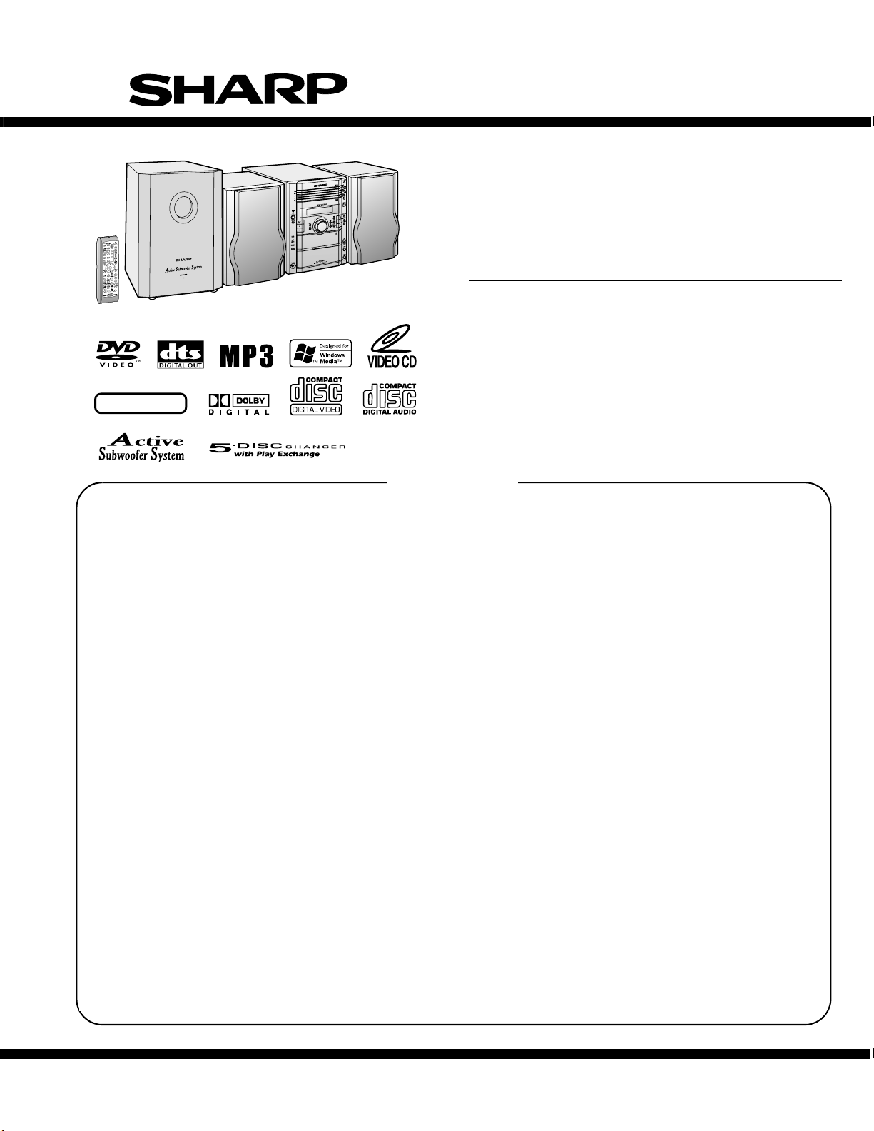
MODEL
XL-DV484W DVD Micro System consisting of XL-DV484W
(main unit), CP-DV484W (front speaker) and CP-SW800V (active subwoofer).
CHAPTER 6. CIRCUIT SCHEMATICS AND PARTS
LAYOUT
[1] NOTES ON SCHEMATIC DIAGRAM ............6-1
[2] TYPES OF TRANSISTOR AND LED ............6-1
[3] WIRING SIDE OF PWB/SCHEMATIC DIA-
GRAM............................................................6-2
CHAPTER 7. FLOWCHART
[1] Troubleshooting.............................................7-1
CHAPTER 8. OTHERS
[1] FUNCTION TABLE OF IC .............................8-1
[2] FL DISPLAY ..................................................8-8
CHAPTER 9. ACTIVE SUBWOOFER DIAGRAM
[1] BLOCK DIAGRAM.........................................9-1
[2] WIRING SIDE OF PWB/SCHEMATIC DIA-
GRAM............................................................9-3
Parts Guide
XL-DV484W
CHAPTER 5. CIRCUIT DESCRIPTION
[1] WAVEFORMS OF DVD CIRCUIT .................. 5-1
[2] VOLTAGE....................................................... 5-2
SHARP CORPORATION
This document has been published to be used
for after sales service only.
The contents are subject to change without notice.
Page 2
XL-DV484W
AudioXL-DV484WService ManualXLDV484WMarketE
CHAPTER 1. GENERAL DESCRIPTION
[1] SAFETY PRECAUTION FOR SERVICE MANUAL
Precaution to be taken when replacing and servicing the Laser Pickup.
The AEL (Accessible Emission Level) of Laser Power Output for this model is specified to be lower than Class 1 Requirements. However, the following precautions must be observed during servicing to protect your eyes against exposure to the Laser beam.
1) When the cabinet has been removed, the power is turned on without a compact disc, and the Pickup is on a position outer than the lead-in position, the Laser will light for several seconds to detect a disc. Do not look into the Pickup Lens.
2) The Laser Power Output of the Pickup inside the unit and replacement service parts have already been adjusted prior to shipping.
3) No adjustment to the Laser Power should be attempted when replacing or servicing the Pickup.
4) Under no circumstances look directly into the Pickup Lens at any time.
5) CAUTION - Use of controls or adjustments, or performance of procedures other than those specified herein may result in hazardous radiation
exposure.
[2] VOLTAGE SELECTION
Before operating the unit on mains, check the preset voltage. If the voltage is different from your local voltage, adjust the voltage as follows.
Turn the selector with a screwdriver until the appropriate voltage number appears in the window(110V,127V,220V or 230V - 240V AC).
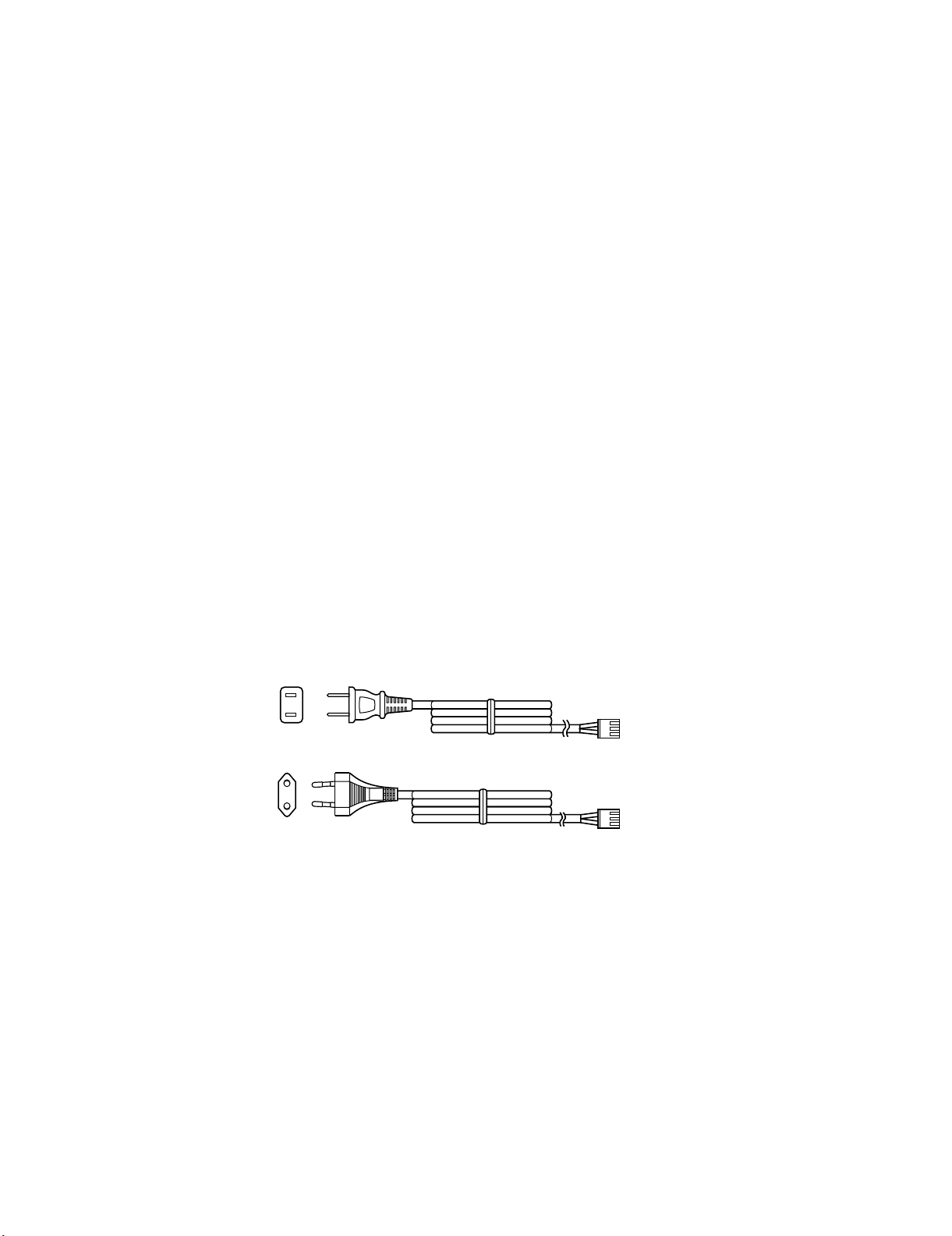
[3] AC POWER SUPPLY CORD AND AC PLUG ADAPTOR
QACCL0008AW00
QACCE0015AW00
1 – 1
Page 3
FOR A COMPLETE DESCRIPTION OF THE OPERATION OF THIS UNIT, PLEASE REFER
TO THE OPERATION MANUAL.
[4] SPECIFICATIONS
XL-DV484W
■ General
Power source AC 110/127/220/230-240 V , 50/60 Hz
Power consumption
Dimensions Width: 185 mm (7-1/4")
Weight
120 W
Height: 260 mm (10-1/4")
Depth: 307 mm (12")
6.4 kg (14.1 lbs.)
■ Amplifier
Output power
Output terminals Speakers: 6 ohms
Input terminals
MPO: 200 W (100 W + 100 W) (10 % T.H.D.)
RMS: 100 W (50 W + 50 W) (10 % T.H.D.)
RMS: 76 W (38 W + 38 W) (0.9 % T.H.D.)
Headphones: 16 - 50 ohms (recommended:
32 ohms)
Subwoofer pre-output (audio signal):
200 mV/10 k ohms at 70 Hz
Video/auxiliary (audio input): 500 mV/47 k ohms
Microphone 1/2: 1 mV/600 ohms
■ Cassette deck
Frequency response 50 - 14,000 Hz (normal tape)
Signal/noise ratio 50 dB (recording/playback)
Wow and flutter 0.3 % (WRMS)
■ DVD/VCD/CD player
Signal system NTSC/PAL
Supported disc types DVD, audio CD, CD-R, CD-RW, VCD, MP3/
Video output Output socket: Pin socket x 1
S-video output Y output level: 1 Vp-p (75 ohms)
Video signal Horizontal resolution: 500 lines
Audio signal Frequency characteristics:
WMA
Output level: 1 Vp-p (75 ohms)
C output level: 0.628 Vp-p (75 ohms)
Output socket: S-video connector x 1
S/N ratio: 60 dB
Linear PCM DVD:
4 Hz to 22 kHz (48 kHz sampling)
4 Hz to 44 kHz (96 kHz sampling)
CD: 4 Hz to 20 kHz
S/N ratio: 96 dB, 1 kHz (CD)
Dynamic range:
96 dB (Linear PCM DVD)
96 dB (CD)
Total harmonic distortion ratio:
0.006 % maximum
■ Tuner
Frequency range FM: 88.0 - 108.0 MHz
AM: 531 - 1,602 kHz
■ Speaker
Type 2-way type speaker system
Maximum input power
Rated input power 50 W
Impedance 6 ohms
Dimensions Width: 165 mm (6-1/2")
Weight 2.5 kg (5.5 lbs.)/each
5 cm (2") tweeter
13 cm (5-1/8") woofer
100 W
Height: 261 mm (10-1/4")
Depth: 200 mm (7-7/8")
■ Active subwoofer
Power source AC 110/127/220/230 - 240 V, 50/60 Hz
Power consumption 83 W
Output power MPO: 332 W (10 % T.H.D.)
Input terminals Subwoofer input (audio signal):
Speaker type 20 cm (7-7/8") woofer
Impedance 6 ohms
Dimensions Width: 220 mm (8-5/8")
Weight 11.5 kg (25.3 lbs.)
RMS: 200 W (10 % T.H.D.)
RMS: 158 W (0.9 % T.H.D.)
200mV/10kohmsat70Hz
Height: 332 mm (13-1/16")
Depth: 415 mm (16-5/16")
Specifications for this model are subject to change without prior
notice.
1 – 2
Page 4
XL-DV484W
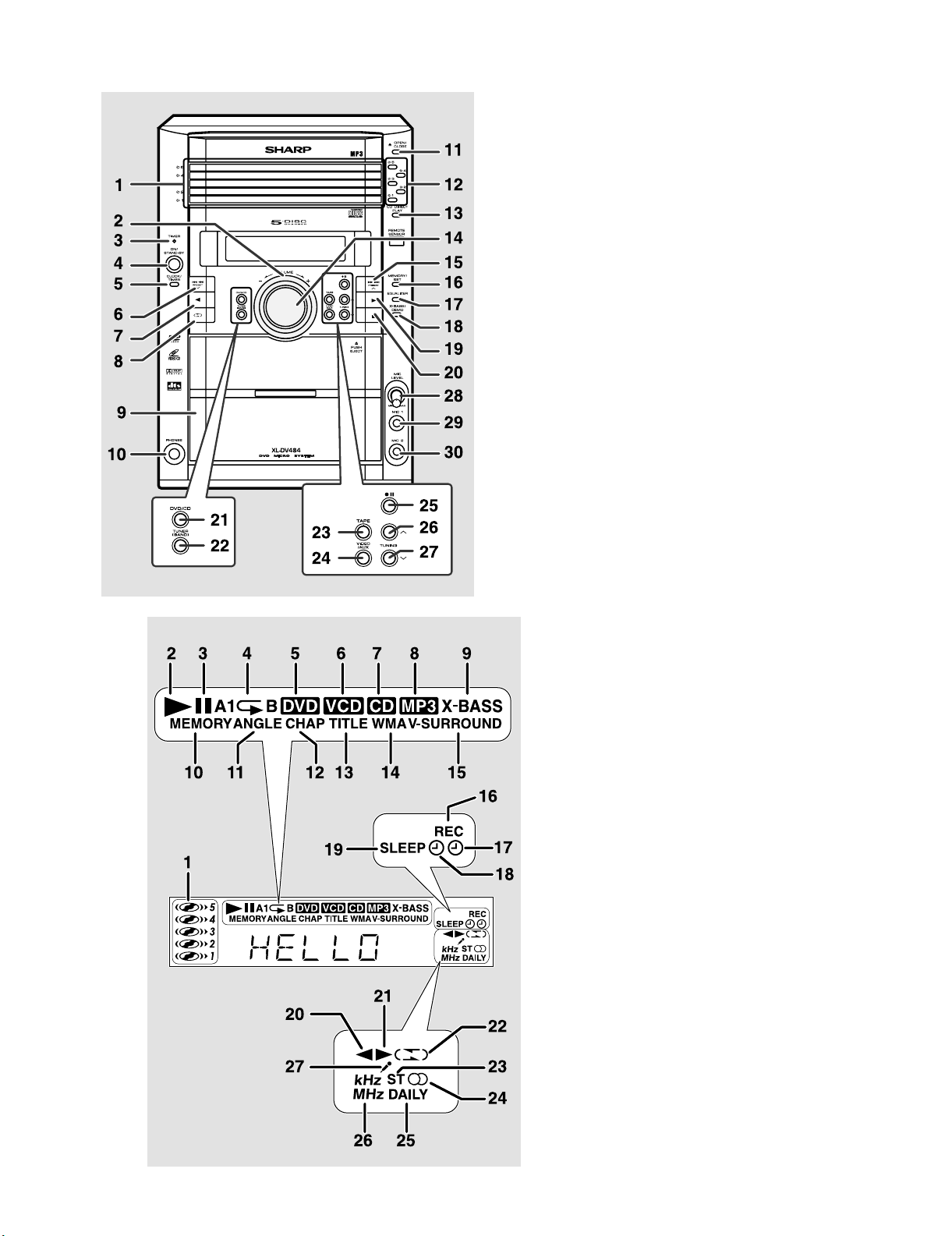
[5] NAMES OF PARTS
Front panel■
1. Disc Trays
2. Illumination Light
3. Timer Set Indicator
4. On/Stand-by Button
5. Clock/Timer Button
6. DVD/Video CD/CD/MP3/WMA Track Down or Fast Reverse, Tape
Fast Wind, Tuner Preset Down, Time Down Button
7. Tape Reverse Play Button
8. Tape Reverse Mode Select Button
9. Cassette Compartment
10. Headphone Socket
11. Disc Tray Open/Close Button
12. Disc Number Select Buttons
13. DVD/Video CD/CD/MP3/WMA Direct Play Button
14. Volume Control
15. DVD/Video CD/CD/MP3/WMA Track Up or Fast Forward, Tape
Fast Wind, Tuner Preset Up, Time Up Button
16. Memory/Set Button
17. Equaliser Mode Select Button
18. Extra Bass/Demo Mode Button
DVD/Video CD/CD/MP3/WMA Play, Tape Forward Play Button
19.
20. DVD/Video CD/CD/MP3/WMA or Tape Stop Button
21. DVD/Video CD/CD/MP3/WMA Button
22. Tuner (Band) Button
23. Tape Button
24. Video/Auxiliary Button
25. Tape Record Pause Button
26. Tuning Up Button
27. Tuning Down Button
Mic Level
28.
29.
Mic 1
Socket
Mic 2
30.
Socket
■ Display
1. Disc Number Indicators
2. DVD/Video CD/CD/MP3/WMA Play Indicator
3. DVD/Video CD/CD/MP3/WMA Pause Indicator
4. DVD/Video CD/CD/MP3/WMA Repeat Indicator
5. DVD Indicator
6. VCD Indicator
7. CD Indicator
8. MP3 Indicator
9. Extra Bass Indicator
10. Memory Indicator
11. DVD Angle Indicator
12. DVD Chapter Indicator
13. DVD Title Indicator
14. WMA Indicator
15. Virtual Surround Indicator
16. Tape Record Indicator
17. Timer Recording Indicator
18. Timer Play Indicator
19. Sleep Indicator
20. Tape Reverse Play Indicator
21. Tape Forward Play Indicator
22. Tape Reverse Mode Indicator
23. FM Stereo Mode Indicator
24. FM Stereo Receiving Indicator
25. Daily Timer Indicator
26. Tuner Receiving Frequency Indicators
27. Karaoke Mode Indicator
1 – 3
Page 5
XL-DV484W
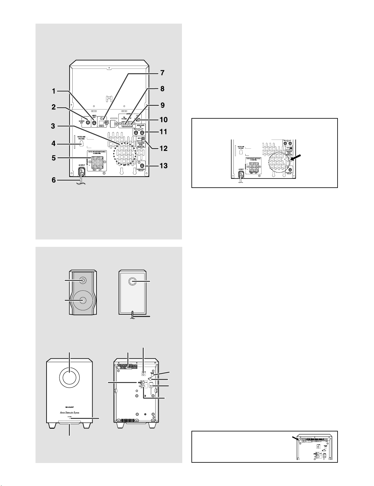
■ Rear panel
1. Video Output Socket
2. S-Video Output Socket
3. Cooling Fan
4. AC Voltage Selector
5. Speaker Terminals
6. AC Power Lead
7. Audio Digital Output Socket
8. FM 75 Ohms Aerial Terminal
9. FM Aerial Earth Terminal
10. AM Loop Aerial Socket
11. Video/Auxiliary (Audio Signal) Input Sockets
12. Span Selector Switch
13. Subwoofer Pre-output Socket
Cooling fan:
This product is equipped with a cooling fan inside, which begins to run at
a specified volume level for better heat radiation.
■ Speaker system
1. Tweeter
2. Woofer
3. Bass Reflex Duct
4. Speaker Wire
1
3
2
4
1
10
2
5
4
6
7
8
9
■ Active subwoofer
1. Bass Reflex Port
2. Power Indicator
3. Subwoofer Unit
4. Cooling Fan
5. Subwoofer Input Socket
6. AC Voltage Selector
7. Power Switch
8. AC Power Lead
9. Volume Control
10. Crossover Frequency Control
3
Cooling fan:
This product is equipped with a cooling fan
inside, which begins to run once the power is
on for better heat radiation.
1 – 4
Page 6
XL-DV484W
11
12 13 14
15
2
3
4
5
6
7
8
9
10
16 17
18
19
1
20
21
22
23
24
25
26
27
28
29 30 31 32
33 34 35 36
37 38 39 40
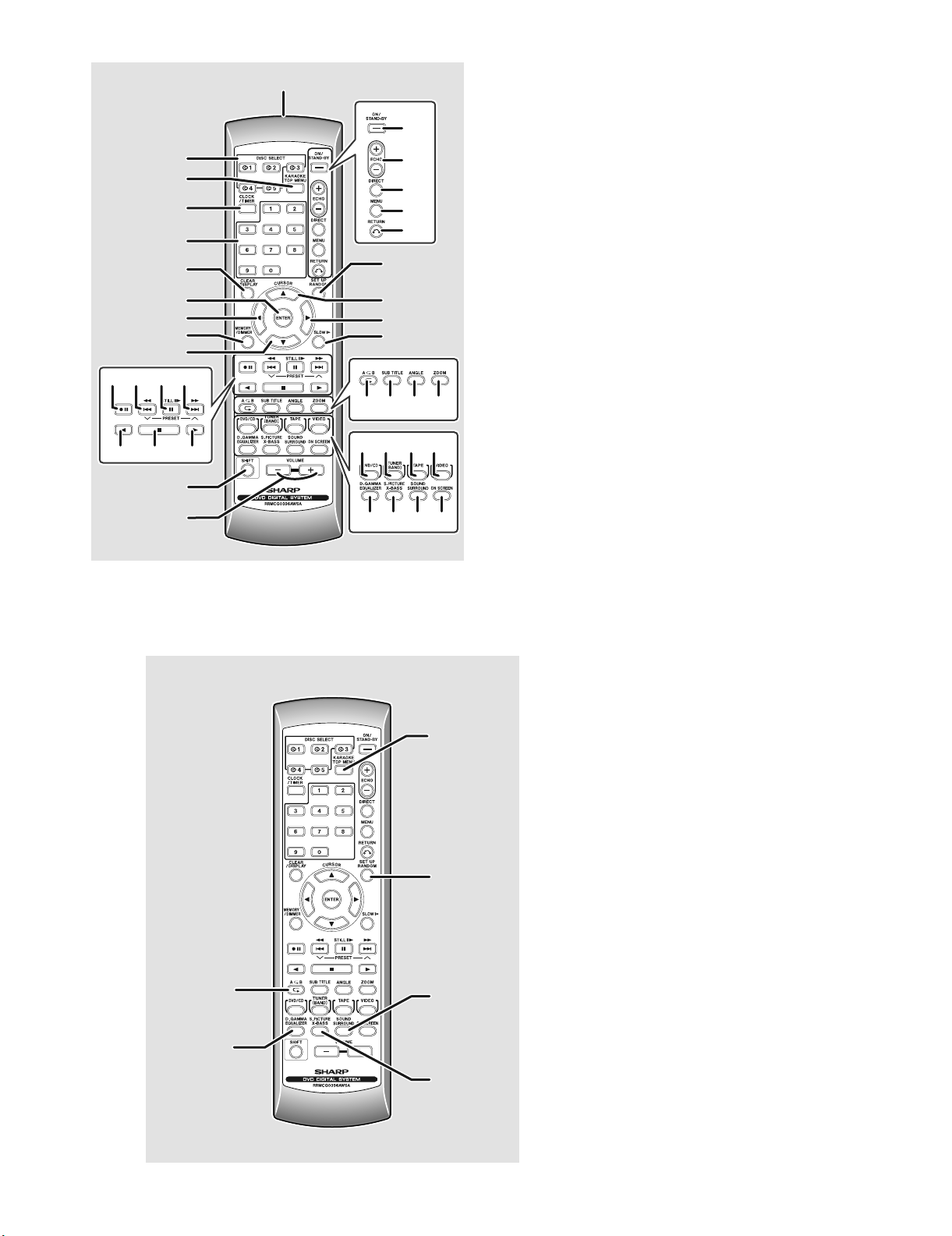
■ Remote control
1. Remote Control Transmitter
2. Disc Number Select Buttons
3. DVD Top Menu Button
4. Clock/Timer Button
5. Direct Search Buttons
6. Clear/Display Button
7. Enter Button
8. Cursor Left Button
9. Memory/Dimmer Button
10. Cursor Down Button
11. Tape Record Pause Button
12.
DVD Chapter Skip/DVD/Video CD/MP3/WMA Fast Reverse/Video CD/
CD/MP3/WMA Track Down/Tape Fast Wind and Tuner Preset Down,
Time Down Button
13. DVD/Video CD/CD/MP3/WMA Pause Button
DVD Chapter Skip/DVD/Video CD/MP3/WMA Fast Forward/Video CD/
14.
CD/MP3/WMA Track Up/Tape Fast Wind and Tuner Preset Up,
Time Up Button
15. Tape Reverse Play Button
16. DVD/Video CD/CD/MP3/WMA/Tape Stop Button
17. DVD/Video CD/CD/MP3/WMA/Tape Play Button
18. Shift Button
19. Volume Up/Down Buttons
20. On/Stand-by Button
21. Echo Level Up/Down Buttons
22. DVD Direct Button
23. DVD Menu Button
24. Return Button
25. CD Random Button
26. Cursor Up Button
27. Cursor Right Button
28. DVD/Video CD Slow Button
29. DVD/Video CD/CD/MP3/WMA Repeat Button
30. DVD Subtitle Button
31. DVD Angle Button
32. DVD Zoom Button
33. DVD/Video CD/CD/MP3/WMA Button
34. Tuner (Band) Button
35. Tape Button
36. Video Button
37. Equaliser Mode Select Button
38. Extra Bass Button
39. DVD 3-D Virtual Surround Button
40. DVD On Screen Button
■ Remote control with shift button
1. Karaoke/Audio Mode Button
2. DVD Setup Button
3. DVD Sound Button
1
4. DVD Super Picture Button
5. DVD/Video CD/CD A-B Repeat Button
6. DVD Digital Gamma Button
2
5
3
6
4
1 – 5
Page 7
AudioXL-DV484WService ManualXLDV484WMarketE
CHAPTER 2. ADJUSTMENTS
XL-DV484W
[1] ADJUSTMENT
1. MECHANISM SECTION
• Driving Force Check
Torque Meter Specified Value
Play: TW-2111 Over 80 g
• Torque Check
Torque Meter Specified Value
Play: TW-2111 30 to 80 g.cm
Fast forward: TW-2231 70 to 180 g.cm
Rewind: TW-2231 70 to 180 g.cm
2. TUNER SECTION
fL: Low-range frequency
fH: High-range frequency
• AM IF/RF
Signal generator: 400 Hz, 30%, AM modulated
Test Stage Frequency Frequency
Display
AM IF 450 kHz 1,602 kHz T351 *1
AM Band
— 531 kHz (fL): T306
Coverage
AM Tracking 990 kHz 990 kHz (fL): T303 *1
Setting/
Adjusting
Parts
1.1 ± 0.1 V
Instrument
Connection
*2
• Tape Speed
Normal
MTT-111 Variable
speed
Test Tape Adjusting
Point
Resistor in
motor.
TAPE MECHANISM
Tape
Motor
Variable Resistor in motor
Figure 1
Specified
Value
Instrument
Connection
3,000 ± 30 Hz Speaker Ter-
minal (Load
resistance: 6
ohms)
*1. Input: Antenna Output: TP302
*2. Input: Antenna Output: TP301
• FM RF
Signal generator: 1 kHz, 40 kHz dev., FM modulated
Test Stage Frequency Frequency
Display
Setting/
Adjusting
Point
FM OSC — 87.50 kHz T301 (fL):
1.3 ± 0.1 V
FM RF 98.00 MHz
98.00 MHz L312 *2
(10-30 dB)
*1. Input: Antenna Output: TP301
*2. Input: Antenna Output: Speaker terminal
• FM IF
Signal generator: 10.7MHz FM modulated
Test Stage Frequency Frequency
Display
Setting/
Adjusting
Point
IF 10.7 MHz 98 MHz T302
(Turn the
core of transformer T302
fully counterclock wise)
Instrument
Connection
*1
Instrument
Connection
*1
TUNER PWB-C
20
IC302
TP301
C393
T351
AM IF
FM ANTENNA
TERMINAL
IC301
T302
FM IF
T301
FM OSC
SO302
L312
FM RF
AM TRACKING fL
T306
AM BAND
COVERAGE fL
IC303
AM
LOOP
ANTENNA
CNP301
R356
TP302
T303
*1. Input: Antenna Output: TP301
Figure 2 ADJUSTMENT POINTS
2 – 1
Page 8

XL-DV484W
3. DVD SECTION
• Adjustment
Since this DVD system incorporates the following automatic adjustment functions, readjustment is not needed when replacing the
pickup. Therefore, different PWBs and pickups can be combined
freely.
Each time a disc is changed, these adjustments are performed
automatically. Therefore, playback of each disc can be performed
under optimum conditions.
Items adjusted automatically
1) Offset adjustment (The offset voltage between the head amplifier
output and the VREF reference voltage is compensated inside the
IC.)
* Focus offset adjustment
* Tracking offset adjustment
2) Tracking balance adjustment
3) Gain adjustment (The gain is compensated inside the IC so that the
loop gain at the gain crossover frequency will be 0 dB.)
* Focus gain adjustment
* Tracking gain adjustment
4. DVD ERROR CODE DESCRIPTION
Error Explanation
10* CAM error. Can't detect CAM switch when CAM is moving.
11* When it detect cam operation error during initialize process.
20* TRAY error. Can't detect TRAY switch when TRAY is mov-
ing.
21* When it detect TRAY operation error during initialize pro-
cess.
30 When it change to DVD function, DVD cannot start up.
* 'CHECKING'
If Error is detected, 'CHECKING' will be displayed instead of 'ERCD**'. 'ER-CD**' display will only be displayed when error had been
detected for the 5th times.
2 – 2
Page 9

[2] TEST MODE
XL-DV484W
3. DVD TEST Mode
1. TEST Mode Functions
1.1. Entering the TEST Mode
While holding down both the button and the X-Bass button ofthe
main unit from the power-off state, press the ON/STAND-BY button
toenter the Test Menu Mode.
1.2. Test mode processing
When entering the TEST Mode, the ROM version are displayed as follows
Version on the FL display: “UD. ****” (****: Version No.)
1.3. TEST Mode Button
Press direct designation button during the version display to enter the
specified TEST Modes as shown below.
No. TEST Mode Direct Designation Button
1 SHIPPING TEST OPEN/CLOSE
2 DVD TEST DVD/CD
3 DVD DISPLAY TEST DISC2
1.4. Canceling TEST Mode
1. Press the ON/STAND-BY button in each TEST Mode to display
“CLEAR AL” except SHIPPING TEST. Then reset and start. (Clear
RAM.)
2. It is neccessary to plug,off the A/C cord after “FINISHED” is displayed on the FL for SHIPPING TEST.
3.1. Outline
• To send key codes of the TEST Mode 1 to the DVD unit to start the
TEST Mode.
• Thereafter the system’s microcomputer only sends key codes to
the DVD unit.
• The main unit operation is started in the same way as the normal
startup of the DVD/CD Function.
• Only monitor (video) output is normally controlled. “MUTE ON”
remained.
• During this TEST Mode, “DVD TEST” is shown on the FL display
and change to “DVD****”. (****:DVD Version)
(Display is shown by OSD. Main unit display not available.)
3.2. TEST Mode Operation
1. The TEST Mode is started in the same way as the normal startup of
the DVD/CD Function. Then the DVD unit is normally started. During the TEST Mode, “DVD****” is continuously displayed.
2. Shipping TEST Mode
2.1. Outline
• ID command for initialization is sent to the DVD unit and EEPROM
in the unit is initialized.
• System micro computrer and DVD changer is initialized.
2.2. TEST Mode Operation
When entering the Shipping TEST Mode:
1. “WAIT” is displayed on the FL display .
2. “FINISHED” shall be kept displaying after initialization is completed.
Manually plug off the A/C cord to get out of the TEST Mode.
When initialization is failed, ”NIT ERR” remains to be shown on the
FL display until plug off the A/C cord.
2.3. Supplementary Note
1. When entering this TEST Mode, it is prohibited to press any key
until the above processing is completed.
2 – 3
Page 10
XL-DV484W
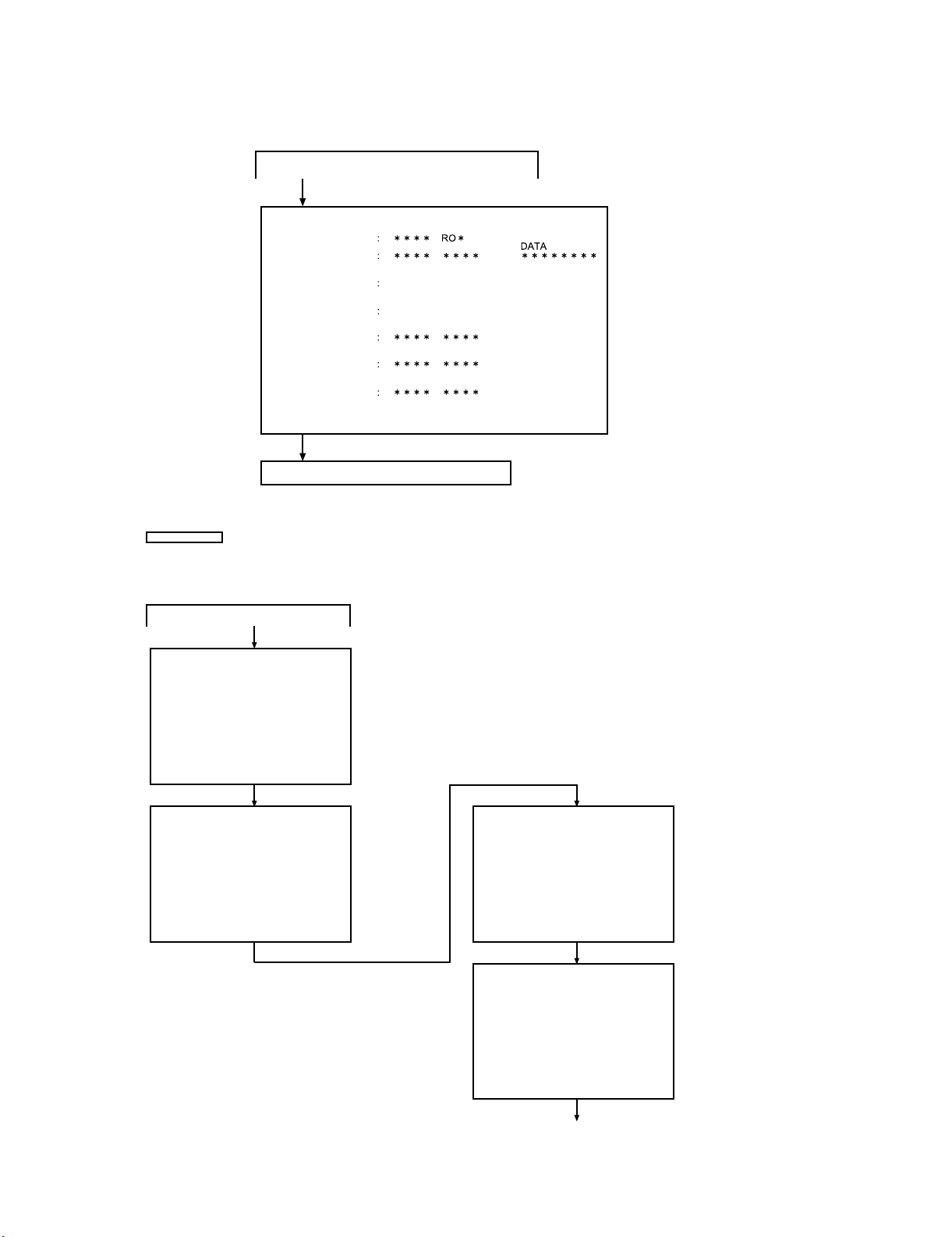
2. DVD TEST Mode
1. Press the DVD/CD button on the main unit from the TEST Mode
initial condition to enter "DVD TEST".
F0000000 00000000
(Press the "1" key of the remote control.)
TEST MODE
Model name (MODEL)
Program version/
Creation date
CPRM key code
(CPRM)
CPRM Serial No.
(S/N)
Microcode
version (UCODE)
Servo program version
(SODCV)
Source code
version (CSTMV)
FFFF FFFF
FFFF FFFFF F
RO*: Region No.
Press the "PLAY" key of the remote control 8 times.
TEST Mode initial screen returns.
LASER TEST Mode
1. Press the DVD/CD button on the main unit from the TEST Mode
initial condition to enter "DVD TEST".
F0000000 00000000
(TEST MODE iitial screen)
(TEST Mode initial screen)
Press the (3) key.
DYNAMIC TEST
1 : LASER TEST
2:STEP TEST
3:PLAY TEST
3:PLAY TESTNOTRAY
MENU:SPIN OFFSET ADJUST
Press the (1) key. Press the (1) key.
LASER TEST
DVD LD ON
The screen display as shown on the left.
The tray opens and
DVD Laser lights on.
The spin rotates
approx. 1 sec.
The pick slightly moves
in the circumference
direction.
LASER TEST
CD LD ON
Press the (1) key.
LASER TEST
LD OFF
DVD laser lights off and
CD laser lights on.
The spin rotates approx.
1 sec.
The pick slightly moves in
the circumference direction.
Laser lights off.
The spin rotates approx.
1 sec.
The pick slightly moves in
the circumference direction.
Press the (1) key to shift to "DVD LD ON".
Press the "STOP" key to return to the "DYNAMIC TEST" screen.
2 – 4
Page 11
Step Execute Mode
1. Press the DVD/CD button on the main unit from the TEST Mode
initial condition to enter "DVD TEST".
XL-DV484W
F0000000 00000000
Press the (3) key.
DYNAMIC TEST
1:LASER TEST
2:STEP TEST
3:PLAY TEST
9:PLAY TEST NO TRAY
MENU : SPIN OFFSET ADJUST
Press the (2) key.
STEP TEST
TRAY OPEN
Press the "PLAY" key.
STEP TEST
FOCUS ON
4-digit alphanumeric
ASMAX
4-digit alphanumeric
FEPP
Press the "PLAY" key.
STEP TEST
TRACK ING ON
4-digit alphanumeric
ASMAX
4-digit alphanumeric
FEPP
4-digit alphanumeric
ASAGC
4-digit alphanumeric
TEAGC
0000
FBAL0
4-digit alphanumeric
TBAL0
Press the "PLAY" key.
STEP TEST
FBAL STUDY
4-digit alphanumeric
ASMAX
4-digit alphanumeric
FEPP
4-digit alphanumeric
ASAGC
4-digit alphanumeric
TEAGC
4-digit alphanumeric
FBAL0
4-digit alphanumeric
TBAL0
Press the "PLAY" key.
STEP TEST
GAIN STUDY
4-digit alphanumeric
ASMAX
4-digit alphanumeric
FEPP
4-digit alphanumeric
ASAGC
4-digit alphanumeric
TEAGC
4-digit alphanumeric
FBAL0
4-digit alphanumeric
TBAL0
4-digit alphanumeric
FCGA0
4-digit alphanumeric
TKGA0
Press the "PLAY" key.
STEP TEST
D V D I D 8-digit numeric
4-digit alphanumeric
ASMAX
4-digit alphanumeric
FEPP
4-digit alphanumeric
ASAGC
4-digit alphanumeric
TEAGC
4-digit alphanumeric
FBAL0
4-digit alphanumeric
TBAL0
4-digit alphanumeric
FCGA0
4-digit alphanumeric
TKGA0
4-digit alphanumeric
FCBT0
4-digit alphanumeric
OFTR0
Press the "STOP" key to return to the DYNAMIC TEST screen.
Turn the power from off to on to clear the Step Execute Mode.
4-digit alphanumeric
4-digit alphanumeric
DVD CD
4-digit alphanumeric
4-digit alphanumeric
ASAGC
TEAGC
FBAL1
TBAL1
4-digit alphanumeric
4-digit alphanumeric
ASAGC
TEAGC
FBAL1
TBAL1
4-digit alphanumeric
4-digit alphanumeric
ASAGC
TEAGC
FBAL1
TBAL1
FCGA1
TKGA1
4-digit alphanumeric
4-digit alphanumeric
ASAGC
TEAGC
FBAL1
TBAL1
FCGA1
TKGA1
FCBT1
OFTR1
(TEST MODE iitial screen)
The screen display as shown on the left.
The tray opens. Put the disc on the tray.
Focus On.
0000
0000
Tracking On.
0000
0000
0000
0000
0000
0000
0000
0000
0000
" ": 4-digit alphanumeric also
displayed for DVD double deck disc.
Focus balance adjustment values displayed.
" ": 4-digit alphanumeric also displayed for
DVD double deck disc.
Focus tracking gain adjustment values displayed.
4-digit alphanumeric also displayed for "****"
in the case of DVD double deck disc.
Equalizer adjustment values and Off-track Level
adjustment values displayed. 8-digit numeric of
DVD ID grows.
" ": 4-digit alphanumeric also displayed
for DVD double deck disc.
Press the "PLAY" key.
STEP TEST
TRACK ING ON
4-digit alphanumeric
ASMAX
4-digit alphanumeric
FEPP
4-digit alphanumeric
ASAGC
4-digit alphanumeric
TEAGC
0000
FBAL0
4-digit alphanumeric
TBAL0
Press the "PLAY" key.
STEP TEST
FBAL STUDY
4-digit alphanumeric
ASMAX
4-digit alphanumeric
FEPP
4-digit alphanumeric
ASAGC
4-digit alphanumeric
TEAGC
4-digit alphanumeric
FBAL0
4-digit alphanumeric
TBAL0
Press the "PLAY" key.
STEP TEST
GAIN STUDY
4-digit alphanumeric
ASMAX
4-digit alphanumeric
FEPP
4-digit alphanumeric
ASAGC
4-digit alphanumeric
TEAGC
4-digit alphanumeric
FBAL0
4-digit alphanumeric
TBAL0
4-digit alphanumeric
FCGA0
4-digit alphanumeric
TKGA0
Press the "PLAY" key.
STEP TEST
C D N O 2-digit numeric T I M E 6-digit numeric
4-digit alphanumeric
ASMAX
4-digit alphanumeric
FEPP
4-digit alphanumeric
ASAGC
4-digit alphanumeric
TEAGC
4-digit alphanumeric
FBAL0
4-digit alphanumeric
TBAL0
4-digit alphanumeric
FCGA0
4-digit alphanumeric
TKGA0
4-digit alphanumeric
FCBT0
4-digit alphanumeric
TEOFS
Press the "STOP" key to return to the DYNAMIC TEST screen.
Turn power from off to on to clear the Step Execute Mode.
4-digit alphanumeric
4-digit alphanumeric
ASAGC
TEAGC
FBAL1
TBAL1
4-digit alphanumeric
4-digit alphanumeric
ASAGC
TEAGC
FBAL1
TBAL1
4-digit alphanumeric
4-digit alphanumeric
ASAGC
TEAGC
FBAL1
TBAL1
FCGA1
TKGA1
4-digit alphanumeric
4-digit alphanumeric
ASAGC
TEAGC
FBAL1
TBAL1
FCGA1
TKGA1
FCBT1
4-digit alphanumeric
TEOFS
0000
0000
0000
0000
0000
0000
0000
0000
Tracking On.
"0000": 4-digit alphanumeric
also displayed for CD-RW.
Focus balance adjustment
values displayed.
"0000": 4-digit alphanumeric
also displayed for CD-RW.
Focus tracking gain adjustment
values displayed.
"0000": 4-digit alphanumeric
also displayed for CD-RW.
Equalizer adjustment value and
TES signal offset displayed.
6-digit numeric of the TIME counter grows.
"0000": 4-digit alphanumeric
also displayed for CD-RW.
2 – 5
Page 12
XL-DV484W
3.3. List of Keys Used for DVD TEST Mode and Transmit Key Codes to the Unit
Button for System
Communication
C-PLAY Play 26h
C-PAUSE/STILL
(Remote Control)
C-STOP (Remote control) Stop 27h
C-STOP (Main Unit) Stop 27h
SKIP-UP/CUE Skip+ 2Ch In this TEST Mode Skip+/Next button code (2Ch) is constantly transferred.
SKIP-DWN/REV Skip- 2Bh In this TEST Mode Skip-/Prev button code (2Bh) is constantly transferred.
SKIP-UP
(Remote Control)
SKIP-DWN
(Remote Control)
REPEAT (Remote Control) Repeat 32h
A-B repeat
(Remote Control)
PROGRAM
(Remote Control)
“1” key (Remote Control) 1 01h
“2” key (Remote Control) 2 02h
“3” key (Remote Control) 3 03h
“4” key (Remote Control) 4 04h
“5” key (Remote Control) 5 05h
“6” key (Remote Control) 6 06h
“7” key (Remote Control) 7 07h
“8” key (Remote Control) 8 08h
“9” key (Remote Control) 9 09h
“0” key (Remote Control) 0 0Ah
ENTER (Remote Control) Enter 70h
MENU (Remote Control) MENU 68h
SLOW> (Remote Control) SLOW> 72h
Button Code Button Code
HEX Value
Pause/still 29h
Skip+ 2Ch
Skip- 2Bh
A-B Repeat 49h
Program 1Fh
Remarks
Buttons used for the TEST Mode are shown above. When pressing the following DVD-related buttons, corresponding button codes are transmitted.
ON SCREEN, SURROUND,CUE, REVIEW, Cursor ↑, ↓, ←, →, RETURN, ZOOM, TOP-MENU, CLEAR, RANDOM subtitle, angle, sound, DVD
MENU, Gamma, S-picture, DIRECT,DISPLAY,SET-UP
3.4. Supplementary Note
1. Do not press buttons other than the DVD-related buttons, except for the ON/STAND-BY button. Do not switch functions; do not control volumes.
For the electronic volume IC and the monitor output control, constantly fix the setting to DVD/CD function.
2 – 6
Page 13

4. ROM Rewrite Mode
Description of version name
Example: VER: VXW0223A
From the left:
V : Video model
X : XLDV***W
W : Southeast Asia
0 223 A : Version
* The format may be changed.
ex) V XW0223A
2 Destination
1 Model
V: Video model/A: Audio/Model for SACD
X : XLDV***W
1 Model
J : Japan
H : Europe
U : USA
K : Korea/Philippines
W : Southeast Asia
A : Australia
Z : Middle East
C : China
M : Mexico
2 Destination
4.1. ROM Rewrite Mode
1. Creating version upgrade disc
• Write the following three files on CD-R/CD-RW.
• !$#%&’().@{}
• D-combo3.cdr
• ********.bin
(********: Names differ according to versions)
• Write the files at lowest possible speed.
• Do not mix other data.
2. During normal power-on, insert the version upgrade disc.
3. After the version upgrade disc is normally determined, the message, “VERSION UP DISC IS DETECTED” and the version are displayed on OSD. Then ROM data read is started.
OSD display (Example)
VERSION UP DISC
IS DETECTED
0905
XL-DV484W
7. Confirming the version
• A few moments after entering the DVD TEST Mode, “DVD ****”
is displayed on the main unit.
(****: 4-digit numeric version code)
• To confirm the detailed version information, press the “1” key of
the remote control.
The system information is displayed on the OSD display.
(“********”: Version name) Check that the version name conforms to the write data.
4. When the data read is completed, “NOW FLASH WRITE START…”
is displayed on OSD. Then the Flash Rom rewrite is entered.
OSD display (Example)
NOW FLASH WRITE START...
5. When rewrite is normally completed, “FL W: END” is displayed on
6. If “FL W:ERR” or “CANT READ” is displayed on the main unit or
the main unit. Eject the disc automatically coming out from the tray.
Then turn the power off.
“FL W:END” is not displayed after 10 minutes, turn the power off to
try again from the start.
ROM DATA READING
956
VERSION UP DISC
IS DETECTED
0905
READ COMPLETE
8. Press the Power button to display “CLEAR AL” .
Reset and start the system’s microcomputer to cancel the test
Mode.
2 – 7
Page 14

XL-DV484W
5. DVD Display Test
5.1. DVD Display Test
To display servo adjustment values, error rates, laser current, etc. during DVD playback.
1. Press the DISC 2 button on the main unit from the TEST Mode initial condition.
2. DVD starts up with “DVD” blinking on the FL display.
3. Press the Tuner/Band button to display DVD adjustment values, etc. Press it again and the display disappears and the normal screen returns.
The error rates displayed are for reference; they are not the judging criteria.
4. Press the “Power” button to cancel this mode.
DVD
FG0 TG0 TG1FG1 FBL0 TBL0 TBL1FBL1
Average error rate
Audio buffer space Video buffer space Number of error occurrence
TitleNo ChapNo
CD
Audio buffer space Video buffer space Number of error occurrence
TrNo TIME
When the Spin Offset Mode is never executed
DVD
FG0
Average error rate
Maximum error rate Laser output
Sector ID
Maximum error rat Laser output
TG0 TG1FG1 FBL0 TBL0 TBL1FBL1
SPIN READ NG
Audio buffer space Video buffer space Number of error occurrence
TitleNo ChapNo Sector ID
CD
Audio buffer space Video buffer space Number of error occurrence
TrNo TIME
2 – 8
Page 15

6. CD-ROM Write Mode
6.1. Outline
DVD-ROM can be upgraded from CD-ROM. The write mode is
entered from the normal mode.
1. When any CD-ROM for version upgrade DVD is detected, the status informs that the version upgrade ROM is being read.
When DVD microcomputer is changed to System microcomputer
and byte 24 status data detects 0Fh:
• The TEST Mode is entered by the status reception.
• The Power button /Function switching is prohibited.
(Power supply is necessary until write is completed.)
• It is prohibited to accept any button input until write is com-
pleted.
• Change the display as follows:
TOC READ
2. To expand into RAM, DVD performs read-operation.
3. When reading ends, transmission stops for writing.
(Ignore stoppage of transmission during write.)
When transmission stops, the transmission port receives write
states, which are displayed according to port states.
W: ***
State Unit display
1 During read FLASH WR
2 During write FL W : S T R
3 Write ended FL W : E N D
4 Write error FL W : E R R
XL-DV484W
4. To open the DVD/CD tray will automatically open when end of
rewrite is detected.
5. To close the DVD/CD door, cancel the TEST Mode and reset when
the ON/STAND-BY button is pressed.
* During write
After reading, “FL W: END” is displayed once. At this point write
does not end. It ends when display is changed from “FL W:
STR” to “W: END” and the DVD/CD tray opens.
* After reading, the DVD/CD tray may open after “W: END” is dis-
played, because RAM is not matched.
Press the Power key to get out of the TEST Mode to read the
version upgrade disc.
6. To initialize the EEPROM, do the shipping TEST mode.
2 – 9
Page 16

XL-DV484W
[3] Standard Specification of Stereo System Error Message Display Contents
Error Contents DISPLAY Notes
DVD DVD Changer Mechanism
Error.
DVD Communication Error. 'ER-CD30' DVD COMMUNICATION ERROR.
Focus Not Match/IL Time Over. 'NO DISC'
TUNER PLL Unlock.
(*) CHECKING:
If DVD changer mechanism error is detected, 'CHECKING' will be display instead of 'ER-CD**'. 'ER-CD**' display will only be display when error had
been detected for the 5 th times.
Speaker abnormal detection and +B PROTECTION display
In case speaker abnormal detection or +B PROTECTION had occurred, it can be check by pressing 'ON/STAND-BY', ' ' and 'X-BASS' button.
MicroComputer version number will displayed as "UD******".
Press ‘VIDEO/AUX’ button during version number display and then press ‘ON/STAND-BY’, ‘MEMORY/SET’ and ‘VIDEO/AUX’ button. Display will
show "S** B**". S is referring to speaker abnormal detection and B is referring to +B PROTECTION. ** is in hex valve.
+B PROTECTION is condition when irregular process occur on power supply line.
BEFORE TRANSPORTING THE UNIT
The following process need to be taken after set tapering/parts replacement.
1. Press the ON/STAND-BY button to enter stand-by mode.
'ER-CD**' (*) 10: CAM SW Detection NG during normal operation
11: CAM SW Detection NG during initialize process
20:TRAY SW Detection NG during normal operation
21:TRAY SW Detection NG during initialize process
87.50
FM MHz
PLL Unlock.
2. While pressing down the button and the X-BASS/DEMO button, press the ON/STAND-BY button. The Micro Computer version number will
be displayed as "UD******".
3. Press OPEN/CLOSE button until "WAIT"--> "FINISHED" appears.
4. Unplug the AC cord and the unit is ready for transporting.
2 – 10
Page 17

Pinch Roller
(B1)x1
<A>
<B>
Pinch
Roller
Pawl
Pull
(D1)x2
Ø2.6x5mm
Motor
Clutch Ass'y
AudioXL-DV484WService ManualXLDV484WMarketE
CHAPTER 3. MECHANICAL DESCRIPTION
XL-DV484W
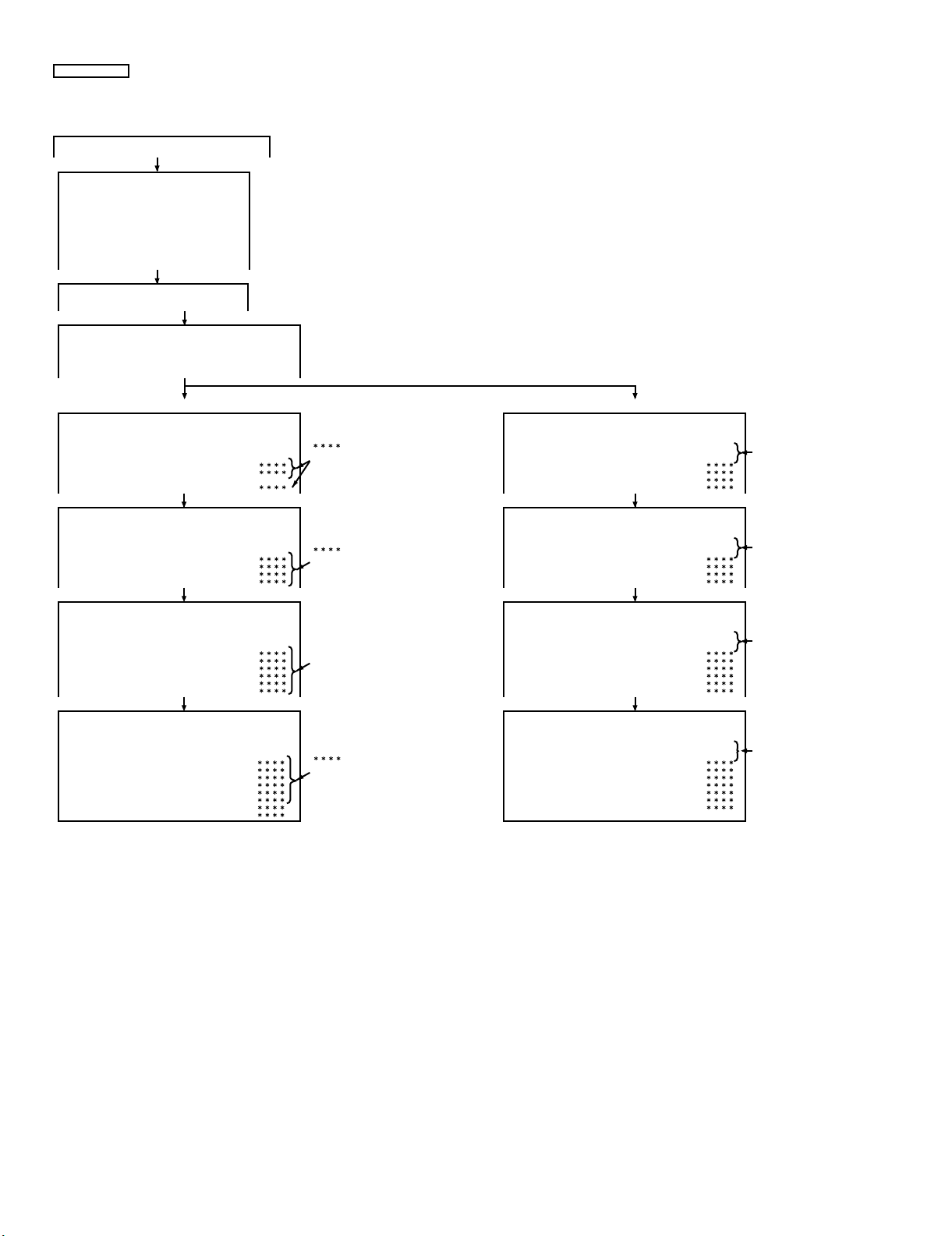
[1] REMOVING AND REINSTALLING THE
MAIN PARTS
1. TAPE MECHANISM SECTION
Perform steps 1 to 11 of the disassembly method to remove the tape
mechanism.(see page 3-3,3-4)
1.1. How to remove the Record/Playback Head (See Fig. 1)
1. When you remove the screws (A1) x 2 pcs and (A2) x 1 pc., the
record/playback head can be removed.
1.2. How to remove the Pinch Roller (See Fig. 2)
1. Carefully bend the pinch roller pawl in the direction of the arrow
<A>, and remove the pinch roller (B1) x 1 pc., in the direction of the
arrow <B>.
NOTE: When installing the pinch roller, pay attention to the spring
mounting position.
1.3. How to remove the Belt (See Fig. 3)
1. Remove the main belt (C1) x 1 pc., from the motor side.
2. Remove the FF/REW belt (C2) x 1 pc.
1.4. How to remove the Motor (See Fig. 4)
1. Remove the screws (D1) x 2 pcs., to remove the motor.
Erase Head
(A1)x2
Ø2x6mm
(A2)x1
Ø2x9mm
Figure 1
Clutch Ass'y
Record/Playback
Head
Main Belt
(C1)x1
Figure 2
FF/REW
Belt
(C2)x1
Figure 3
FF/REW
Clutch
Flywheel
Motor
Figure 4
3 – 1
Page 18

XL-DV484W
1
24
PICKUP UNIT ASS'Y
Short land
Circuit shorted
Circuit open
2. DVD/CD MECHANISM SECTION
2.1. Replacing the DVD mechanism (See Fig. 1)
Before the replacement, unsolder the service DVD pickup short land.
2.2. How to remove DVD/CD Disc (See Fig. 2~6)
1. When DVD/CD is at play position, rotate reduction gear C clockwise as shown in Figure 2 Until disk tray is at ‘STOCK’ position,
then rotate the gear further to eject the disk tray (Figure 6) so that
DVD/CD can be removed from the tray.
2. In another case, if DVD/CD mechanism is at tray No. 1 play position and to remove DVD/CD located in tray No. 3, the procedure is
as follows:
If the gear up down board is located at tray No. 1 position, then
rotate Reduction gear C clock-wise until Disc tray is at stalk
‘STOCK’ position. Rotate reduction gear D clock-wise (Figure 3) to
move the DVD/CD mechanism to tray No. 3 position. This is confirmed by checking the gear up down board position Base on the
marking as indicated on the main chassis as shown in Figure 4.
• Usually changer is covered with top plate. As for reference purpose, we exclude the top plate for easy viewing. (Figure 5,6)
CD Disc
Disc Tray
Guide Tray
Figure 1
Reduction gear C
CD Disc
CD Disc
Remove CD from tray.
CD At play position.
CD At 'STOCK' position.
Figure 5
Tray eject
Gear up down board
Front
Rear
Figure 2
Reduction gear D
Up Down
Figure 3
Figure 6
3 – 2
Figure 4
Mark 1
(DISC 1)
Mark 2 Mark 4
(DISC 2)
Mark 3 Mark 5
(DISC 3)
(DISC 5)
(DISC 4)
Page 19

(A1) x1
ø3x10mm
(A1) x2
ø3x8mm
(A1) x1
ø3x10mm
(A1) x1
ø3x8mm
(A1) x2
ø3x8mm
(B1) x2
ø3x10mm
(A1) x2
ø3x8mm
(A1) x2
ø3x8mm
Front Panel
Cabinet
Rear
Panel Bottom
Rear
Panel Top
Jack PWB
(D1) x9
ø3x8mm
(F1) x1
ø3x8mm
(G1) x1
ø3x10mm
(E1) x1
ø3x10mm
(E2) x1
(C3) x2
(C2) x1
Front Panel
Rear
Panel Bottom
Hook
(C1)x1
Hook
(C1)x1
Pull
Pull
DVD Changer
Unit
Main PWB
Headphones
PWB
Translation PWB
(F2) x1
(E1) x2
ø3x10mm
Front Panel
Turner PWB
MIC PWB
Main PWB
(E2) x1
(C3) x1
Pull
(E3) x1
Tape
Mechanism
(E3) x1
Pull
Hook
(E4)x1
Hook
(E4)x1
[2] DISASSEMBLY
Caution on Disassembly
Follow the below-mentioned notes when disassembling the unit and
reassembling it, to keep it safe and ensure excellent performance:
1) Take cassette tape and compact disc out of the unit.
2) Be sure to remove the power supply plug from the wall outlet
before starting to disassemble the unit.
3) Take off nylon bands or wire holders where they need to be
removed when disassembling the unit. After servicing the unit,
be sure to rearrange the leads where they were before disassembling.
4) Take sufficient care on static electricity of integrated circuits and
other circuits when servicing.
STEP REMOVAL PROCEDURE FIGURE
1 Cabinet 1. Screw..........................(A1) x11 1
2 Rear Panel Top 1. Screw............................(B1) x2 1
3 DVD Changer
unit
4 Rear Panel
Bottom
5 Front Panel 1. Screw...........................(E1) x3
6 Tuner PWB 1. Screw............................(F1) x1
7 Main PWB 1. Screw...........................(G1) x2
8 Power PWB 1. Screw...........................(H1) x4 4
9 Terminal PWB 1. Screw............................(J1) x1 4
10 Display PWB 1. Knob.............................(K1) x1
11 Tape Mechanism 1. Screw...........................(L1) x 4 5
12 Headphones
PWB
13 Mic PWB 1. Knob.............................(N1) x1
14 Translation PWB 1. Screw............................(P1) x1
14 DVD PWB
(Note 1)
15 DVD Mechanism 1. Screw...........................(R1) x4
Note 1:
After removing the connector for the optical pickup from the connector,
wrap the conductive aluminium foil around the front end of the connector so as to protect the optical pickup from electrostatic damage.
1. Hook.............................(C1) x2
2. Flat Cable.....................(C2) x1
3. Socket..........................(C3) x3
1. Screw...........................(D1) x9 2
2. Flat Cable....................(E2) x2
3. Socket..........................(E3) x2
4. Hook............................(E4) x2
2. Socket..........................(F2) x1
2. Socket.........................(G2) x4
2. Screw...........................(K2) x 8
3. Flat Cable....................(K3) x 1
1. Screw..........................(M1) x 1 5
2. Screw..........................(N2) x 1
2. Flat Cable....................(P2) x 2
1. Screw...........................(Q1) x3
2. Socket.........................(Q2) x 1
3. Flat Cable.....................(Q3) x2
2. Screw...........................(R2) x4
2
2,3
2,3
3
2
3
2,4
4
5
5
6
6
6
7
XL-DV484W
Figure 1
Figure 2
Figure 3
3 – 3
Page 20

XL-DV484W
(R2) x2
ø2x12mm
(R2) x2
ø2x10mm
DVD Changer
Unit
DVD Mechanism
Holder
(G2) x2
Main PWB
(H1) x4
ø4x6mm
(G1) x1
ø3x6mm
(G2) x2
Power PWB
(K1) x1
Cassette
Holder
(N1) x1
MIC PWB
Display PWB
Front Panel
(N2) x1
ø3x10mm
DVD Changer
Unit
Figure 4
(L1) x4
ø3x10mm
Figure 5
Terminal PWB
(K3) x1
(K2) x8
ø2.6x8mm
Tape
Mechanism
Headphones
PWB
(M1) x1
ø3x10mm
(J1) x1
ø3x6mm
Figure 7
STEP REMOVAL PROCEDURE FIGURE
1Woofer/
Tweeter
1. Net Frame................(A1) x1
2. Catching Holder.......(A2) x4
3. Screw.......................(A3) x4
4. Front Panel..............(A4) x1
5. Screw.......................(A5) x6
Tweeter
Front Panel
(A4)x1
(A5)x2
ø3.5x14mm
(A5)x4
ø3.5x14mm
Woofer
Net Frame
(A1)x1
(A3)x2
ø3.5x16mm
(A2)x2
8
(R1) x2
ø3x10mm
(Q1) x3
ø3x10mm
(Q2) x2
DVD PWB
Figure 6
(Q3) x1
(R1) x2
ø3x10mm
Translation PWB
(P2) x1
(P1) x1
ø3x10mm
(P2) x1
3 – 4
(A2)x2
(A3)x2
ø3.5x16mm
Figure 8
Screwdriver
Page 21

—MEMO—
XL-DV484W
3 – 5
Page 22

XL-DV484W
Y
AudioXL-DV484WService ManualXLDV484WMarketE
CHAPTER 4. DIAGRAMS
[1] BLOCK DIAGRAM
FM ANTENNA
AM LOOP
ANTENNA
JK1/2
MIC JACK
VRK1
MIC LEVEL
FROM DVD SECTION
REC /P.B. HEAD
L-CH
TAPE
R-CH
AC BIAS
ERASE
HEAD
TERMINAL
SO302
CNP301
2
1
MIC IN
MIC1OUT
MIC2OUT
SWITCHING
Q101Q104
B.P.F
BF301
4
9
12
13
M65856SP
MIC AMP.
CNP601
1
2
3
SWITCHING
Q105
Q106
FM RF
LATCH
7
8
L(TA)
R(TA)
LREC
RREC
Q112
TRACKING
40
DATA
CLOCK
ROUT
LOUT
RIN
LIN
VCC
22
ICK1
+B5
SWITCHING
FM FRONT END
1
384
L312 T301
AM
T303 T306
42
41
35
36
32
31
23
2
23
REC
9
16
11
12
15
Q114
IC301
TA7358AP
7
5
FM OSC
AM BAND
COVERAGE
+B5
QK1
P.B
H/N
SWITCHING
Q113
FM IF
R
L
OSC
BUFF
Q302
VT
20 22 11171615
+B5
Q360
ICK2
CF303T302
4.5 MHZ
FM
OPE AMP.
TJM4558CD
6
9
PLL(TUNER)
FM+B
SWITCHING
6
5
2
3
IC302
LC72131
7
1
+B5
JK690
L
VIDEO/AUX
R
+B5
13
4
L
PB
21
R
L
REC
7
18
R
IC101
AN7345K
PLAYBACK AND RECORD
/PLAYBACK AMP.
+B5
BIAS
OSC
Q111
L103
Q109
SWITCHING
AM OSC OUT
X352
OSC
21
AM MIX
AM OSC IN
7
TAPE
TUNER
DVD/CD
Q605
Q606
BIAS
Q110
T351
CF352
AM IF
OUT
21
7
STEREO
AM RF IN
CE
MO/ST
FM/AM
9
10
8
L
9
R
16
L
10
15
R
L
11
AUDIO PROCESSOR
14
R
L
12
R
13
718
CD
ATT
BIAS
4
98517
GND
AM IF
FM/AM
OUT
18
CLK
DO
DI
5413
6
21
17
IC601
LC75341
Q107
Q108
MUTING
10.7 MHz
CF351
FM
DET
VCC
MPXIN
162324
+B5
3
REC/PLAY
X351
456 kHz
13
14
L
VCO
MO/ST
R
15
FM/AM
12
20
DI
CE
CLK
23
+B5
+B_PROTECT
TO IC701
+B5
ZD351
5.1V
IC303
LA1832S
FM IF DET.
FM MPX./AM IF
1
2
24
–20dB
ATT
R
21
L
4
TO DVD SECTION
DVD_PROTECT
DVD_FUNC
Q601
Q602 Q604
A_+10V
+B5
+B7(SW_+5V)
+B8(DVD_+8V)
DVD_1.5V
DVD_A3.3V
DVD_D3.3V
DVD_A5V
DVD_S5V
+B10
Q603
Q860
MUTE
SYSTEM
AC_RL
Figure 4-1 BLOCK DIAGRAM (1/3)
4 – 1
Page 23

SYSTEM
03
04
V
)
60
MUTE
AC_RLY
+B10
+B5
IC851
AN80T53
MULTI
REGULATOR
GND
5.1V
8.5V
10V
4
IC852
KIA7808AP
VOLTAGE
REGULATOR
IC856
LD1117V
VOLTAGE
REGULATOR
IC855
LD1117V33
VOLTAGE
REGULATOR
–VF
VF2
VF1
P_IN
NC
UNSW_5.6V
PHOTO
TO DVD SECTION
DVD_FUNC
LED701
Q711
LED708
LED707
SW
VCC
35671
Q719
Q710
1
L
R
15
13V
2
+B3
SP DET
IC901
STK432-070
POWER AMP.
GND
13
–VCC
+VCC
9
8
IC853
BD9701T
1CH DC-DC
CONVERTER
25
Q853
IC854
AN78L05
VOLTAGE
REGULATOR
FL701
FL DISPLAY
+B10
4443
VDD
T_SOL
T_MOTOR
IC701
IXA004AW
VDD
+B10
Q907
32 413128
78
69
TUN_SM/SPAN
REMOCON
VOL_JOG1/DSA_DATA
VOL_JOG2/DSA_ACK
DVD + B PRT
CLKDIDO
242115121176
17 18 19 2034
Q905
PT801
POWER
TRANSFORMER
(MAIN)
T.F
AVDD
VOL_JOG/
PROTECT
RESET
SP_RLY
CE
DRIVER
L841
LINE
FILTER
Q906
RL914
RELAY
110V
27
13
25
40
39
34
33
31
8
9
30
29
10
56
53
47
127V
NEUTRAL
2121 4445
5
PHOTO
KARA_LATCH
60
MIC_SW
59
DSA_DATA
8
DSA_ACK
9
62
MOT_A+
MOT_A-
MPEG_PWR
66
68
MO_SPEED
DISCTYPE
67
FUNC_DVD
61
VLOAD
79
P_IN
36
SMUTE
41
TIME LED
42
VOL_LED
45
ILLU_LED
58
80
83
84
100
VDD
12 16
+B10
7
L-OUT
R-OUT
10
1
3
Q866
+B9
48
3837 46
AC_RLY
MOT_B+
MOT_B-
SYSTEM MICROCOMPUTER
T_REC/PLAY
T_BIAS
-20dBATT
XL700
4.19403MHz
T4.0A L 250V
T4.0A L 250V
T2.0A L 250V
T2.0A L 250V
Q801
VOLTAGE
REGULATOR
+B9
F801
F802
F803
F804
Q901
Q904
–B2
+B2
D802
SOLENOID
Q701,702
Q712~715
DVDPROT
FAN MOTOR
M971
+B3
230-240V
220V
SW801
VOLTAGE
SELECTOR
CNP805
LIFE
MOTOR/
DRIVER
+B3
REMOTE SENSOR
+B10
VOLUME
+B_PROTECT
Q703
M
JK701
HEADPHONES
3
22
131
TAPE
MECHANISM
ASS'Y
SW601
SPAN
SELECTOR
RX701
1
2
3
KEY
SW701-SW705
SW709-SW721
KEY
SW722-SW728
VR701
RESET
+B7(SW_5V)
JK953
SUB WOOFER
PRE-OUT
BROWN
BLUE
+B7(SW_+5V)
+B10
TO DVD SECTION
SO901
SPEAKER TERMINAL
AC POWER
SUPPLY CORD
AC 110/127/220/
230-240V,50/60Hz
XL-DV484W
+B10
Figure 4-2 BLOCK DIAGRAM (2/3)
4 – 2
Page 24

XL-DV484W
4
P
V
D3.3V
A5V
IC501
3
2
1
AUDIO
DIGITAL
OUT
DVD/CD
SO7001
S-VIDEO
OUT
JK7002
VIDEO
OUT
M2
MAIN CAM
MOTOR
M
M
M1
TRAY
MOTOR
FROM MAIN PWB
FROM MAIN PWB
CN3203
14
13
12
11
10
CN3201
10
11
CN3003
10
11
12
13
CN3004
SPDIF
1
DGND
2
3
D3.3V
MUTE
TXD
DGND
RXD
PROGRESSIVE
9
ASPECT
VGND
8
Py_OUT
7
Pb_OUT
6
Pr_OUT
5
VGND
4
V_OUT
3
C_OUT
2
1
CAM–
1
CAM+
2
TR–
3
TR+
4
DVD_CS
5
DVD_CLK
6
SYS_DATA
7
DVD_DATA
8
DVD A_MUTE
9
RESET
RXD_CTL_IN
R–CH
1
AUDIO_GND
2
L–CH
3
M_GND
4
A_5V
5
D_GND
6
+8V
7
S_5V
8
S_5V
9
A_GND
D_1.5V
A3.3V
D3.3V
A_5V
+8V
S_5V
D1.5V
A3.3V
D3.3V
Q3100
Q3101
Q3102
IC3003
TC7WT126
BUFFER IC (DVD)
D3.3V
VOLTAGE
DETECTION
D3.3V
IC3503,IC3504
20
TCLV573T
8 bit LATCH IC
D3.3V
1,7,8
IC3002
BD4825G
A0-A15
5
8
7
D/A CONVERTER
1,10
6
IC3801
PCM1748E
94
DGNDAUDIO
GND
Q3501
D3.3V
IC3501
IXA173WJ
FLASH ROM
27,46
131412
14
15
16
13
D3.3V
ADAC_DA
NEXOENEXCENEXWEFADT(0-20)
ADAC_CK
ADAC_L
768FS
IECOUT
181
RXD
DAC1OUT
DAC4OUT
DAC5OUT
RXD_CLT_IN
P15(RXD_CLT)
D_3.3V
52
158
163
164
DVD_CS
60
S_CLK
53
S_DIN
55
S_DOUT
54
AMUTE
94
NRST
68
59
47
43,49,55,75,81
1,3,9,15,29,35,41
NRAS
NCSM
NWE
NCAS
MDQ(0-31)
MCK
IC3401
IX0614AW
IX0614AW(HY57V643220CT-7)
64M SD-RAM
6,12,32,38,44,46,52
58,72,78,84,86
D_GND
14
15
IC3601
1,12D3.3V
BU2363FV
CLOCK
GENERATOR
10
2,11
DQM(0-3)
MA(0-11)
873
974817296
S
DI
BA(0-1)
D_3.3V
8
Figure 4-3 BLOCK DIAGRAM (3/3)
4 – 3
D_GND
X3601
Page 25

XL-DV484W
FG
-7)
D_3.3V
IC3001
IXA464AW
SERVO/SIGNAL
CONTROL
VIDEO/AUDIO
DIGITAL SIGNAL
PROCESSOR
49,92,170
104,118,145,149
153,157,165
A3.3V
IC3602
BR24L04F
8
4K bit EEPROM
1-4,7
7
VCC
S_5V
SPIN
31-34
VHALF
VCC
M_8V
FG
SPIN
66
58,69,80,93,99,169
177,183,194,198,206
211,215,221,224,230
236,241,245,248,254
218,226,233,240,250
62
63
P3(SCL)
P2(SDA)
6
5
VHALF
146
137
73,71,70
152,150
106,119,138
151,155,159,167
4,11,16,24,30,43
1,7,14,23,29,42
56,79,91,171,182
189,195,202,209
15,67,98,186
213,222,244
121-131
134,136
133,135
LPCO1
LPCO2
A_GND
D_GND
D3.3V
D1.5V
74
Q3305
Q3306
Q3303
Q3304
25
9,27,28
D3301
A_GND
8
IC3704
LA6261
FOCUS/TRACKING
SPIN/SLED DRIVER
18
12
16
14
29
S_5V
IC3301
7SB3157P
BUS SWITCH
A_GND
Q3307
DVD_H
5,6
IC3702
NJM12904
OPE.AMP.
1
1,2
35,36
L
H
4
2,3
3,4
7,26
M_GND
S_5V
PD_CD
A_GND
SPIN–
SPIN+
5,6
CN3301
1
2
3
4
5
6
7
8
9
10
11
12
13
14
15
16
17
18
19
20
21
22
23
24
A_3.3V
GND
LD_DVD
NC
VOSC
PDMON
LD(CD)
VR(DVD)
VR(CD)
NC
VE
VCC
Vref
G(PDIC)
VF
VB
VA
RF
CD/DVD
VD
VC
TR–
TR+
FO+
FO–
D_GND
DVD MECHANISM
SPIN–
SPIN+
IN SW
SL–
SL+
AGND
FG
LED
UNIT ASS'Y
M
SPINDLE
MOTOR
M
SENSOR
PWB
PICKUP
UNIT ASSY
SLED
MOTOR
Figure 4-3 BLOCK DIAGRAM (3/3)
4 – 4
Page 26

XL-DV484W
AudioXL-DV484WService ManualXLDV484WMarketE
CHAPTER 5. CIRCUIT DESCRIPTION
[1] WAVEFORMS OF DVD CIRCUIT
DVD_CS IN
1
S_DIN
2
S_D OUT
3
SCLK OUT
4
5 – 1
Page 27

[2] VOLTAGE
XL-DV484W
PIN
NO.
PIN
NO.
PIN
NO.
PIN
NO.
1
2
3
4
5
6
7
8
9
10
11
12
13
14
15
16
17
18
19
20
21
22
23
24
1
2
3
4
5
6
7
8
9
1
2
3
4
5
6
7
8
9
10
11
12
13
14
15
16
17
18
19
20
21
22
1
2
3
4
5
6
7
8
9
10
11
12
13
14
15
16
17
18
19
20
21
22
23
24
IC101
VOLTAGE
0V
0V
0.58 V
1.97 V
0V
0V
0V
0.59 V
3.39 V
3.37 V
0V
0V
6.87 V
4.14 V
0V
3.37 V
0.59 V
0V
0V
0V
1.99 V
0.58 V
0V
0V
IC301
VOLTAGE
0.87 V
1.58 V
5.42 V
1.56 V
0V
5.44 V
4.70 V
5.39 V
5.44 V
IC302
VOLTAGE
2.52 V
0V
0V
0V
4.75 V
5.08 V
0V
4.69 V
3.87 V
3.98 V
5.12 V
2.57 V
4.72 V
0V
0V
2.40 V
5.13 V
0.92 V
0.92 V
1.35 V
0V
2.56 V
IC303
VOLTAGE
2.10 V
5.03 V
2.10 V
2.10 V
0.00 V
5.08 V
5.05 V
2.90 V
5.02 V
4.37 V
3.87 V
3.87 V
3.99 V
1.25 V
1.98 V
2.09 V
2.68 V
2.34 V
0V
0V
2.41 V
2.41 V
5.03 V
3.50 V
PIN
NO.
PIN
NO.
PIN
NO.
PIN
NO.
PIN
NO.
PIN
NO.
PIN
NO.
1
2
3
4
5
6
7
8
9
10
11
12
13
14
15
16
17
18
19
20
21
22
23
24
1
2
3
4
5
6
7
8
9
10
11
12
13
14
15
1
2
3
4
5
6
7
1
2
3
1
2
3
4
5
1
2
3
1
2
3
IC601
VOLTAGE
0V
0V
0V
4.19 V
4.16 V
4.17 V
4.17 V
4.19 V
4.17 V
4.17 V
4.17 V
4.17 V
4.17 V
4.17 V
4.17 V
4.17 V
4.20 V
4.17 V
4.17 V
4.16 V
4.19 V
4.19 V
8.36 V
0V
IC901
VOLTAGE
-0.15 V
-0.15 V
-
36.90 V
-35.5 V
0V
0V
38.10 V
-38.2 V
0V
0V
-37.0 V
0V
-0.15 V
-0.15 V
IC851
VOLTAGE
5.06 V
12.80 V
18.28 V
0V
17.42 V
9.90 V
8.36 V
IC852
VOLTAGE
18.26 V
0V
7.98 V
IC853
VOLTAGE
18.28 V
0V
0V
0.98 V
17.10 V
IC855
VOLTAGE
5.00 V
3.69 V
0V
IC856
VOLTAGE
3.45 V
1.74 V
0V
ICK1
PIN
VOLTAGE
NO.
10.81V
2
1.0 V
3
0.74 V
4
2.47 V
562.45 V
2.46 V
7
2.46 V
2.46 V
8
2.46 V
9
10 2.46 V
11 2.46 V
12 2.46 V
13
2.46 V
14 2.46 V
15
2.46 V
16
2.46 V
17 2.46 V
18
2.46 V
19 2.46 V
20 0.53 V
21 0.53 V
22 0 V
23 0 V
24 0 V
25 0 V
26 0 V
27
2.46 V
28 2.46 V
29 2.46 V
30 2.46 V
31 2.43 V
32 2.43 V
33 2.46 V
34 2.46 V
35 2.46 V
2.46 V
36
2.46 V
37
2.46 V
38
2.46 V
39
0V
40
4.87 V
41
0V
42
ICK2
PIN
VOLTAGE
NO.
1
5.24 V
5.24 V
2
3
5.24 V
4
0V
5
5.24 V
6
5.24 V
7
5.24 V
8
9.62 V
PIN
VOLTAGE
NO.
13.5V
22.6V
3
3.5 V
4
2.3 V
52.3V
60V
72.3V
82.8V
9
3.5 V
10 2.2 V
11 2.2 V
12 0 V
13 2.5 V
14 2.4 V
15
3.5 V
16 2 V
17 3.4 V
18 3.4 V
3.3 V
19
20 3.1 V
21
0V
1.6 V
22
1.6 V
23
24
0V
25
0V
26
0V
27
2V
28
3.5 V
29
0.6 V
30
2.6 V
31 0 V
32332.3 V
2.3 V
34 3.5 V
35 2.3 V
36
2.8 V
37 0 V
38 2.2 V
2.2 V
39
40 3.5 V
41 2.5 V
42 3.5 V
43 0 V
44 2.6 V
45
0V
46 2.3 V
47 2.3 V
3.5 V
48
49 2.3 V
50 2.8 V
IC3401
PIN
VOLTAGE
NO.
51 0 V
52
2.2 V
2.2 V
53
3.5 V
54
55 2.5 V
56 0 V
57 0 V
58592V
1.7 V
60 1.6 V
61 1.8 V
62 1.7 V
63 2.9 V
64 0 V
65 0 V
66 3.5 V
67 1.8 V
68 0 V
69 0 V
70 2 V
71 0 V
72 0 V
73 2.6 V
74 3.5 V
75 2.3 V
76 0 V
77 2.3 V
78 2.8 V
79 3.5 V
80 2.2 V
81 2.2 V
82 0 V
83 2.5 V
84 0 V
85 0 V
86 0 V
Q110
PIN
VOLTAGE
NO.
0V
1
9.84 V
2
0V
3
Q302
PIN
VOLTAGE
NO.
0.88 V
E
2.52 V
C
0V
B
Q601
PIN
VOLTAGE
NO.
0V
E
0V
C
0.71 V
B
Q602
PIN
VOLTAGE
NO.
0V
E
0V
C
0.71 V
B
Q603
PIN
VOLTAGE
NO.
0V
E
0V
C
0.66 V
B
IC3704
PIN
VOLTAGE
NO.
11.2V
2
1.2 V
3
0V
4
0V
561.4 V
1.7 V
7
0V
0V
8
0V
9
10 7.6 V
11 0 V
12 0 V
13
1.3 V
14 1.3 V
15
0V
16
0V
17 0.7 V
18
0.7 V
19 7.6 V
20 1.3 V
21 1.3 V
22 7.6 V
23 1.3 V
24 7.6 V
25 1.2 V
26 1.2 V
27
0V
28 1.2 V
29 1.2 V
30 1.2 V
31 1.2 V
32 1.2 V
33 1.2 V
34 1.2 V
35 1.2 V
36 1.2 V
Q604
PIN
VOLTAGE
NO.
0V
E
0V
C
0.66 V
B
Q605
PIN
VOLTAGE
NO.
0V
E
0V
C
12.80 V
B
Q606
PIN
VOLTAGE
NO.
0V
E
0V
C
0.69 V
B
Q701
PIN
VOLTAGE
NO.
12.94 V
E
0V
C
12.94 V
B
Q702
PIN
VOLTAGE
NO.
12.94 V
E
1.10 V
C
12.94 V
B
PIN
NO.
PIN
NO.
PIN
NO.
PIN
NO.
PIN
NO.
PIN
NO.
PIN
NO.
PIN
NO.
PIN
NO.
PIN
NO.
PIN
NO.
PIN
NO.
PIN
NO.
PIN
NO.
1
2
3
1
2
3
E
C
B
E
C
B
E
C
B
E
C
B
1
2
3
E
C
B
E
C
B
1
2
3
E
C
B
E
C
B
E
C
B
E
C
B
Q710
VOLTAGE
0V
0V
4.37 V
Q711
VOLTAGE
9.89 V
9.98 V
0.88 V
Q712
VOLTAGE
0.90 V
4.83 V
0.90 V
Q713
VOLTAGE
12.94 V
0.88 V
12.94 V
Q714
VOLTAGE
0V
4.83 V
0V
Q715
VOLTAGE
12.94 V
1.10 V
12.94 V
Q719
VOLTAGE
0V
5.03 V
0V
Q853
VOLTAGE
0V
8.53 V
0V
Q860
VOLTAGE
0V
4.76 V
0V
Q866
VOLTAGE
0V
17.05 V
0V
Q901
VOLTAGE
0V
4.82 V
0V
Q902
VOLTAGE
0V
4.82 V
0V
Q903
VOLTAGE
0V
4.82 V
0V
Q904
VOLTAGE
0V
4.82 V
0V
PIN
NO.
PIN
NO.
PIN
NO.
E
C
B
E
C
B
E
C
B
Q906
VOLTAGE
0V
2.30 V
0V
Q907
VOLTAGE
0V
4.85 V
0.62 V
QK1
VOLTAGE
4.86 V
7.85 V
5.52 V
5 – 2
Page 28

XL-DV484W
PIN
VOLTAGE
NO.
1 3.5 V
2 2.5 V
3
2.5 V
4
0V
5 2.7 V
6 2.3 V
7 3.5 V
8 3.5 V
9
2.3 V
10 2.3 V
11 0 V
12 2.6 V
13 2.6 V
14 3.5 V
15
1.3 V
16 0 V
17 0 V
18 3.5 V
2.7 V
19
20 0.8 V
21
2.7 V
2.7 V
22
3.5 V
23
0V
24
3.1 V
25
0V
26
27
0.5 V
28
0.5 V
29
3.5 V
0V
30
31 2.8 V
32330.7 V
2.9 V
34 2.7 V
35 2.6 V
36
0.7 V
37 2.6 V
38 0 V
0V
39
40 0.5 V
41 0.7 V
42 3.5 V
43 0 V
44 2.7 V
45
0.7 V
46 2.9 V
47 3.4 V
0V
48
49 0 V
50 0 V
PIN
VOLTAGE
NO.
51 0 V
3.4 V
52
3.3 V
53
3.3 V
54
55 2.7 V
56 3.5 V
57 0 V
58590V
0V
60 2.4 V
61 3.4 V
62 3.4 V
63 3.4 V
64 1.7 V
65 0 V
66 2.9 V
67 1.3 V
68 3.1 V
69 0 V
70 1.7 V
71 1.7 V
72 0 V
73 0 V
74 3.4 V
75 3.4 V
76 3.4 V
77 3.4 V
78 1.7 V
79 3.5 V
80 0 V
81 3.4 V
82 0 V
83 3.4 V
84 0 V
85 0 V
86 0 V
87 0 V
88 0 V
0V
89
0V
90
91 3.5 V
92 1.7 V
93 0 V
94 0 V
95 3.4 V
96 0 V
97
0V
98
1.3 V
99 0 V
100 0 V
PIN
VOLTAGE
NO.
101 3.4 V
102
0V
0V
103
3.4 V
104
105 0.9 V
106 0 V
107 0.8 V
108
1.6 V
2.1 V
109
110 2.6 V
111 2.1 V
112 1.1 V
113 2 V
114 1.6 V
115 1.6 V
116 1.6 V
117 1 V
118 3.5 V
119 0 V
120 1 V
121 1.7 V
122 2.1 V
123 2.1 V
124 2.1 V
125 2.1 V
126 2.1 V
127 2.1 V
128 2.1 V
129 2.1 V
130 2.1 V
131 2.1 V
132 0 V
133 0 V
134 0 V
135 0 V
136 2.1 V
137 1.7 V
138 0 V
1.7 V
139
1.7 V
140
141 1.7 V
142 1.7 V
143 0 V
144 1.4 V
145 3.4 V
146 1.7 V
147 2.3 V
148 2.3 V
149 3.4 V
1.7 V
150
IC3001
PIN
NO.
151 0 V
152
153
154
155 2.2 V
156 3.4 V
157 0.7 V
158
159
160 3.4 V
161 1.4 V
162 0.7 V
163 1.7 V
164 3.4 V
165 1.4 V
166 0 V
167 2.2 V
168 0 V
169 1.6 V
170 3.4 V
171 1.7 V
172 3.4 V
173 1.7 V
174 2.7 V
175 1.7 V
176 1.7 V
177 0 V
178 0 V
179 0 V
180 0 V
181 1.7 V
182 3.5 V
183 0 V
184 2.6 V
185 2.5 V
186 1.3 V
187 2.2 V
188 1.3 V
189
190
191 2.3 V
192 2.3 V
193 2.8 V
194 0 V
195 3.5 V
196 2.8 V
197 2.3 V
198 0 V
199 2.2 V
200 2.3 V
VOLTAGE
1.7 V
1.3 V
0V
0V
3.4 V
3.5 V
2.3 V
PIN
VOLTAGE
NO.
201 2.2 V
202
3.5 V
2.3 V
203
2.5 V
204
205 2.6 V
206 0 V
207 2 V
208
2V
3.4 V
209
210 1.7 V
211 0 V
212 1.6 V
213 1.3 V
214 0 V
215 0 V
216 1.7 V
217 0 V
218 3.4 V
219 1.6 V
220 0 V
221 0 V
222 1.3 V
223 1.8 V
224 0 V
225 1 V
226 3.5 V
227 0 V
228 0 V
229 0 V
230 0 V
231 0 V
232 3.4 V
233 3.4 V
234 0 V
235 0 V
236 0 V
237 3.5 V
238 3.5 V
3.5 V
239
3.5 V
240
241 0 V
242 3.5 V
243 3.5 V
244 1.3 V
245 0 V
246 3.5 V
247 3.5 V
248 0 V
249 3.5 V
250 3.5 V
PIN
VOLTAGE
NO.
251 3.5 V
3.5 V
252
3.5 V
253
0V
254
255 3.5 V
256 3.5 V
IC3801
PIN
VOLTAGE
NO.
11.7V
0V
2
1.7 V
3
4
0V
5
3.5 V
64.7V
72.3V
82.3V
0V
9
10 2.3 V
11 3.5 V
12 3.5 V
13 0 V
14 0 V
3.5 V
15
16 1.7 V
IC3503
PIN
VOLTAGE
NO.
10V
2.6 V
2
0.6 V
3
4
0.5 V
5
0.7 V
6 2.7 V
7 2.7 V
8 0.5 V
0.5 V
9
10 0 V
11 0 V
12 0 V
13 0 V
14 0 V
0V
15
16 0 V
17 0 V
18 0 V
19 0 V
20 0 V
IC3504
PIN
VOLTAGE
NO.
10V
2.8 V
2
2.8 V
3
4
0.5 V
5
0.7 V
6 0.7 V
7 0.7 V
8 2.8 V
2.8 V
9
10 0 V
11 12 -
13 14 -
-
15
16 -
17 18 -
19 -
20 -
IC3601
PIN
VOLTAGE
NO.
1 3.5 V
0V
2
1.7 V
3
4
1.7 V
5
3.5 V
60V
7 1.7 V
8 1.7 V
1.7 V
9
10 1.7 V
11 0 V
12 3.5 V
13 1.7 V
14 0 V
15 1.7 V
16 3.5 V
IC3602
PIN
VOLTAGE
NO.
1
0V
0V
2
3
0V
0V
4
3.5 V
5
6 3.5 V
70V
8 3.5 V
IC3702
PIN
VOLTAGE
NO.
1
1.7 V
1.7 V
2
3
1.7 V
0V
4
2.8 V
5
63.1V
70V
84.8V
IC3501
PIN
VOLTAGE
NO.
1 0.4 V
2 0.5 V
3
2.6 V
4
2.8 V
5 0.7 V
6 0.5 V
7 0.7 V
8 2.7 V
9
0V
10 0 V
11 3.5 V
12 3.1 V
13 0 V
14 3.5 V
15
0V
16 0 V
17 0 V
18 2.7 V
2.9 V
19
20 2.6 V
21
0.8 V
22
0.7 V
23
0.7 V
24
2.8 V
25
2.9 V
26
2.9 V
27
0V
28
2.9 V
29
2.8 V
2.6 V
30
31 2.8 V
32330.6 V
0.7 V
34 0.5 V
35 0.7 V
36
0.7 V
37 3.5 V
38 0.7 V
2.7 V
39
40 2.6 V
41 2.6 V
42 2.8 V
43 0.5 V
44 2.7 V
45
0.5 V
46 0 V
47 3.5 V
2.7 V
48
5 – 3
Page 29

AudioXL-DV484WService ManualXLDV484WMarketE
CHAPTER 6. CIRCUIT SCHEMATICS AND PARTS LAYOUT
[1] NOTES ON SCHEMATIC DIAGRAM
XL-DV484W
•Resistor:
To differentiate the units of resistors, such symbol as K and M are
used: the symbol K means 1000 ohm and the symbol M means
1000 kohm and the resistor without any symbol is ohm-type resistor. Besides, the one with “Fusible” is a fuse type.
• Capacitor:
To indicate the unit of capacitor, a symbol P is used: this symbol P
means pico-farad and the unit of the capacitor without such a symbol is microfarad. As to electrolytic capacitor, the expression
“capacitance/withstand voltage” is used.
(CH), (TH), (RH), (UJ): Temperature compensation
(ML): Mylar type
(P.P.): Polypropylene type
• Schematic diagram and Wiring Side of P.W.Board for this model
are subject to change for improvement without prior notice.
XL-DV484W
REF. NO DESCRIPTION POSITION
SW1 CLAMP ON—OFF
SW2 TRAY SW1 ON—OFF
SW3 TRAY SW2 ON—OFF
SW4 DISC ON—OFF
SW601 SPAN SELECTOR 50/9
SW701 ON/STAND-BY ON—OFF
SW702 CLOCK/TIMER ON—OFF
SW703 REVERSE MODE ON—OFF
SW704 REVERSE PLAY ON—OFF
SW705 PRESET DOWN ON—OFF
SW709 DVD/CD ON—OFF
SW710 TUNER (BAND) ON—OFF
SW711 VIDEO/AUX ON—OFF
SW712 TAPE ON—OFF
SW713 REC/PAUSE ON—OFF
SW714 TUNING/TIME UP ON—OFF
SW715 TUNING/TIME DOWN ON—OFF
• The indicated voltage in each section is the one measured by Digital Multimeter between such a section and the chassis with no signal given.
1. In the tuner section,
indicates AM
indicates FM stereo
2. In the main section, a tape is being played back.
3. In the deck section, a tape is being played back.
4. In the power section, a tape is being played back.
5. In the CD section, the CD is stopped.
• Parts marked with “ ” ( ) are important for
maintaining the safety of the set. Be sure to replace these parts
with specified ones for maintaining the safety and performance of
the set.
REF. NO DESCRIPTION POSITION
SW716 STOP ON—OFF
SW717 PLAY ON—OFF
SW718 PRESET UP ON—OFF
SW719 X-BASS/DEMO ON—OFF
SW720 EQUALISER ON—OFF
SW721 MEMORY/SET ON—OFF
SW722 DIRECT PLAY ON—OFF
SW723 DISC 1 ON—OFF
SW724 DISC 2 ON—OFF
SW725 DISC 3 ON—OFF
SW726 DISC 4 ON—OFF
SW727 DISC 5 ON—OFF
SW728 OPEN/CLOSE ON—OFF
SW801 VOLTAGE SELECTOR 230-240V
CP-SW800V
REF. NO DESCRIPTION POSITION
SW801 VOLTAGE SELECTOR ON—OFF
SW802 Power ON—OFF
[2] TYPES OF TRANSISTOR AND LED
FRONT
VIEW
EC B
(S) (G) (D)
(1) (2) (3)
KTC3203 Y
KTA1271 Y
KTA1273 Y
KTA1274 Y
KTC3194 Y
KTC3200 GR
KTC3199 GR
B
(3)
E
TOP
VIEW
(1)
KTA1298 Y
KTA1504 GR
KTC3875 GR
KRC104 S
KRC107 S
KRC102 S
6 – 1
C
(2)
KRA102 S
KRA107 S
KRC107 S
KTA1298 Y
2SD601 AR
2SB709 AR
FRONT
VIEW
SVC347S
SVC230C
Page 30

XL-DV484W
C
C
[3] WIRING SIDE OF PWB/SCHEMATIC DIAGRAM
A
B
C
D
E
F
G
6-11 12 - G
FROM DVD PWB
TAPE MECHANISM
Ass'y(211)
ERASE HEAD
R-CH
L-CH
RECORD/
PLAYBACK HEAD
HEAD PLATE
BLOCK(211-1)
CNW3004
(2/3)
CNS102
6
5
4
3
2
1
6
5
4
3
2
1
6-2 1 - D
TO MAIN PWB(1/3)
6-2 1 - E~G
TO MAIN PWB(2/2)
1
2
3
1
2
3
4
5
6
7
8
9
10
11
12
13
22
21
20
20
12
7
29
11
30
8
7
6
5
4
3
2
1
MAIN PWB-A1(1/2)
L-CH
A_GND
R-CH
CNP601
DVD_RCH
DVD_A_GND
DVD_LCH
DVD_MGND
DVD_A5V
DVD_DGND
LD+8V
DVD_S5V
DVD_S5V
DVD_AGND
DVD_1.5V
DVD_A3.3V
DVD_D3.3V
DVD_D3.3V
DVD_A3.3V
DVD_1.5V
DVD_AGND
DVD_S5V
DVD+8V
DVD_DGND
DVD_A5V
DVD_MGND
BI102
ERASE
M_GND
T2_R2
A_GND
T2_R1
T2_L1
T2_L2
+B
+B
+B
+B
FM SIGNAL
CD/DVD AUDIO SIGNAL
MIC SIGNAL
PLAYBACK SIGNAL
AUX SIGNAL
RECORD SIGNAL
C609
R605
10K
R116
56
C114
0.033
R118 R120
100K
–
+
Hich=T1
+
–
R117
100K 3.9K
R115
56
15K
R607
R119
C115
560P
4.7K
C116
560P
3.9K
112K
112K
1/50
C607
0.15
C611
0.0022
4.7/50
3.9K
R609
+B
R122
3.3K
R124
6.8K
C118
47/25
54321
R123
C117
47/25
6.8K
3.3K
R121
R613
390
R611
2.2K
Q601
KTC3875 GR
Q602
R610
2.2K
KTC3875 GR
390
R612
R645
10K
R646
10K
22K
22K
R621
C639
2.2/50
150
R149
C141
100/16
3.4V
3
1
3
3.4V
15K
C112
0V
0.0015
C106
Q106
KTC3199 GR
0V
0.0015
0V
C105
100/16
C110
R114
330P
1K
24 23 22 21 20
C109
R113
330P
1K
C113
0.033
C111
100/16
R111
Q603
KTC3875 GR
R146
9.3V
9.3V
KTA1504 GR
Q102
KTC3200 GR
R104
2.2K
0.7V
0.7V
Q104
KTC3200 GR
Q103
KTC3200 GR
0.7V
R105
3.3K
0.7V
Q101
KTC3200 GR
8.6V
R106
3.3K
Q604
Q112
R103
2.2K
KTC3875 GR
C645
1/50
C646
1/50
R617
2.2K
R616
2.2K
R147
R148
4.7K
6.8K
R615
6.8K
R614
C640
R620
22/50
Q113
KRC104 S
10K10K
0V
2
0V
1
0V
2
Q114
KRC104 S
R112
R108
47K
0V
0V
4.7K
R110
4.7K
Q105
R109
KTC3199 GR
0V
R107
47K
R619
330
R618
330
+B
+B
+B
0V
0V
C104
0V
180P(CH)
C103
0V
180P
(CH)
0V
0V
220P
C652
1
2
3
4
5
C605
0.15
6
C613
1/50
7
C615
8
1/50
C617
9
1/50
C619
10
C621
1/50
11
12
C623
1/50
KTC3875 GR
C625
0.0022
68K
R150
SPARE
R128
6789
0.022
C121
1K
R601
R602
1K
220P
C651
LC75341
AUDIO PROCESSOR
DI
CE
INTERFACE
VSS
LOUT
–
+
LBASS
LTRE
LIN
LSEL0
L4
L3
L2
L1
R126
5.6K
3.3/50
C143
R647
2.2K
Q605
Q108
0V
270P
8.2K
C124
Hich=CHROME
5.6K
R129
C123
270P
8.2K
R127
–
+
–
+
R649
4.7K
220K
R136
REC_R
KTC3875 GR
0.7V
R132
1.5K
R130
C126
22/16
–
+
+
–
C125
1.5K
R133
R131
C127
IC601
CCB
AUX
DECK
TUNER
CD
R138
100
C128
0.022
56K
22/16
100
0.022
56K
–
+
R648
2.2K
0.0033
C130
16171819
0.0033
C129
–
+
+
–
–
+
R139
10K10K
10K
R134
C132
47/25
10 11 12
C131
47/25
R135
–
+
0.7V
ALC
22/16
C133
Nor/CrO2
10K
CLK
VDD
VREF
ROUT
RBASS
RTRE
RIN
RSEL0
R4
R3
R2
R1
Q606
KTC3875 GR
R650
4.7K
220/10
C134
+B
131415
VCC
RIPPLE
ALC
IC101
C653
220P
24
23
22
21
20
19
18
4.
17
16
15
14
13
Q107
KTC3875 GR
0V
0.022
C135
AN7345K
PLAYBACK AND RECORD/
H
NOTES ON SCHEMATIC DIAGRAM can be found on page 6-1
1
23456
Figure 6-2 SCHEMATIC DIAGRAM (1/17)
6 – 2
Page 31

XL-DV484W
1
ESSOR
–
+
+
–
–
+
648
.2K
R139
R134
C132
47/25
6
10 11 12
C131
+
10K
0.7V
10K
47/25
R135
–
ALC
10K
CLK
VDD
VREF
ROUT
RBASS
RTRE
RSEL0
Q606
KTC3875 GR
R650
4.7K
22/16
220/10
C133
C134
131415
RIPPLE
Nor/CrO2
ALC
IC101
C653
220P
24
23
22
21
20
19
RIN
18
17
R4
16
R3
15
R2
14
R1
13
Q107
0V
+B
VCC
AN7345K
+B
C606
0.15
C614
1/50
C616
4.7/50
C620
1/50
C622
1/50
KTC3875 GR
0.022
R158
220
C135
R142
82
(1/2W)
R143
47K
PLAYBACK AND RECORD/
PLAYBACK AMP.
C603
22/16
C618
1/50
0V
C137
C608
0.15
C601
220/16
MIC_IN(R)
C624
1/50
C626
0.0022
11.6V
R144
22K
0.0082
0.047(ML)
C610
1/50
R606
4.7K
3.9K
R608
R137
11.6V
Q109
KTA1504 GR
0V
0V
0V
C138
C139
0.039(ML)
C602
0.022
C612
0.0022
MIC_OUT(R)
220K
+B
R145
4.7
L103
Q111
+B
0V
KTC3203 Y
330µH
R604
10K
R140
R141
47K
4.7K
R603
1K
KRC104 S
2
C140
47/25
Q110
R693
M_+13V
C691
390P
C690
390P
SW_+5V
39K
R692
39K
TUN_R
A_GND
TUN_L
D_GND
A_+10V
+B
DO
CLK
DI
CE
CNP303
MIC_OUT(L)
MIC_IN(L)
A_GND
MIC_OUT(R)
MIC_IN(R)
A_+10V
D_GND
KARA LATCH
MIC IN
D_GND
SW601
SPAN
SELECTOR
DVD PROTECT
DVD FUCTION
MIC SWITCH
KARA LATCH
TUN_SM/SPAN
UNSW5.6
P_IN
SP_RLY
SP_DET
CLK
+B_PROTECT
D_GND
S_MUTE
T_BIAS
REC/PLAY
–20dB
M_+13V
SW_5V
A_+10V
–VF
–VF
VF1
DISC TYPE
VF2
CNP701B
R691
3.9K
R690
3.9K
R642
10K
R644
3.3K
A_GND
+B
+B
+B
A_+10V
+B_PROTECT
DVD PROT
DVD_FUNC
+B
+B
+B
D_GND
UNSW5.6V
1727242625 101615 14 13
TO MAIN PWB(2/2)
6-4 1 - D~G
SP_RLY
4519 23 698
SP_DET
P_IN
R643
3.3K
R641
10K
3
1
M_GND
TAPE_A_GND
4
3
2
1
CLK
BIK1
DI
DO
CE
VF1
VF2
14
13
12
11
10
DI
10
11
12
29
28
27
26
25
24
23
22
21
20
19
18
17
16
15
14
13
12
11
10
JK690
L-CH
VIDEO/AUX
R-CH
CHASSIS
GND
9
8
7
6
5
4
3
2
1
1
2
3
4
5
6
7
8
9
50/9
100/10
29
9
8
7
6
5
4
3
2
1
1
TO DISPLAY PWB
CNS303
6-15 10 - H
FFC701
CNP701A
6-7 11 - B
FROM TUNER PWB
CNSK1
10
11
1
2
3
4
5
6
CNPK1
6-17 11 - E
7
8
9
TO MIC PWB
7
8 9 10 11 12
Figure 6-3 SCHEMATIC DIAGRAM (2/17)
6 – 3
Page 32

XL-DV484W
S
8
C
2
H
G
N
9
9
56K
56K
56K
C921
2200/56
C922
2200/56
1
C851
Q866
KRC107 S
L
R
0.1(ML)
L
R
R874
10K
FM SIGNAL
L901
0.29µH
L902
0.29µH
C926
0.22
C928
0.22
R940
4.7
(1/4W)
–B
–Vcc
GND
+B
Vcc
+B
C866
47/25
+B
0.1
C884
C961
C868
(1/4W)
220/35
C927
0.22
C929
0.22
R941
4.7
6800/35
UNSW_5.6V
+B
+B
+B
+B
LG2(231)
VF2
VF1
–VF
P_IN
LG1(231)
680
1
2
3
4
5
6
7
8
9
BI801
1
2
3
4
5
6
7
BI802
R
(
R
6
(1/
D
KT
C
C
C
L-CH
R909
1K
R905
C909
22/16
C903
0.001
R901
56K
0.22/50
+B
DVD_PROTECT
DVD_1.5V
DVD_A3.3V
DVD_D3.3V
DVD_FUNC
A_GND
M_GND
TAPE A GND
D_GND
DVD_AGND
DVD_DGND
DVD_MGND
Ch1
820
+B
+B
+
–
100(1/4W)
R907
56K
3P(CH)
C905
R925
C913
100/63
R921
22K
LG3(231)
(50 watts/Ch)
Ch1
Out
+Vcc
0.22
(2W)
R917
0.22
(2W)
R919
C932
0.22
R923
Q901
KTC3875 GR
+B
+B
+B
22K
R853
+B
C882
47/25
C878
47/25
+B
1K
D862
DS1SS133
0.1
C881
+B
0.1(ML)
C877
+B
+B
+B
L
R913
0.1
(1W)
C911
0.022
R915
5.6K
C902
0.22/50
+B
+B
HEATSINK
A
C907
470P
R903
1K
B
C901
C
L_CH
1
A_GND
2
D
3
4
5
6
7
8
9
R_CH
SP_RLY
SP_DET
M_+13V
DVD_+8V
A_+10V
+B_PROTECT
E
SW_+5V
10
DVD_A5V
11
DVD_S5V
12
TO MAIN SECTION
F
6-3 2-B/2-E/6-3 8~11 - H
G
VF2
13
VF1
14
–VF
15
P_IN
16
UNSW5.6V
17
19
20
21
22
23
24
25
26
27
28
29
30
C915
10/63
D905
DS1SS133
+B
D861
DS1SS133
2
R881
120
R882
47
2
R875
330
R876
27
(2Ch)
Out
Ch2
–Vcc
(2W)
0.22
R920
–B
R914
C916
10/63
(1W)
C912
0.022
FAN MOTOR 5V
+B
22K
R864
C864
22/25
Q860
KTC3875 GR
D860
DS1SS133
IC856
3
1
LD1117V
(1.5V)
VOLTAGE
REGULATOR
3
1
IC855
LD1117V33
VOLTAGE
REGULATOR
0.22
R918
0.1
R916
5.6K
56K
R902
MULTI REGULATOR
10V
ZD860
DZ11BSB
D868
DS1SS133
R-CH
+
Ch2
–
151413121110987654321
C908
(2W)
C914
100/63
DS1SS133
1K
R924
8.5V
C859
22/25
C879
C880
10/50
C875
R
D906
Q902
C904
0.001
IC851
AN80T53
5.1V
C865
22/25
R859
10K
0.1
D883
D882
C876
10/50
470P
22/16
0.1
D865
C872
(ML)
820
R906
56K
R908
D907
DS1SS133
Q904
C946
0.1/50
VCC
MODE 1
3.3K
R854
Q853
2
KRC104 S
3
ZD804
DZ6.8BSB
1SS133
R866
2.2K
R867
470/10
1.8K
R865
1K
R910
KTC3875 GR
SW
C854
220/25
1
1K
C906
3P(CH)
13V
+B
100µH
R922
100(1/4W)
C910
KTC3875 GR
4356172
GND
C874
C855
10/50
R857
22K
RL204F
RL204F
0.1
IC901
STK432-070
POWER AMP.
1K
R904
Q903
KTC3875 GR
REGULATOR
C867
22/25
C852
0.1(ML)
IC853
BD9701T
1CH DC-DC
L801
CONVERTER
21
4
3
D1FH3
D866
R935
R936
R937
C925
47/50
+B
22K
R927
22K
R928
IC852
KIA7808AP
VOLTAGE
3
2
5
H
NOTES ON SCHEMATIC DIAGRAM can be found on page 6-1
1
23456
Figure 6-4 SCHEMATIC DIAGRAM (3/17)
6 – 4
Page 33

XL-DV484W
/
C961
AL
C927
0.22
C929
0.22
R941
4.7
(1/4W)
c
D
c
6800/35
35
220
+B
+B
+B
+B
LG2(231)
VF2
VF1
–VF
P_IN
UNSW_5.6V
LG1(231)
R958
(1/2W)
680
R957
680
(1/2W)
D911
DS1SS133
Q905
KTC3875 GR
CHASSIS
GND
1
1
2
3
2
4
3
4
5
6
5
6
7
8
7
8
9
CNS801
BI801
1
1
2
3
2
4
3
4
5
5
6
6
7
BI802
CHASSIS
GND
0.2V
CNS802
1
2
3
4
5
6
7
8
CNP801
VF2
1
VF1
2
–VF
3
P_IN
4
5
6
CNP802
C861
R942
(1/2W)
680
R945
2.2K
R943
(1/2W)
680
L_OUT
R_OUT
RL914
RELAY
4.4V
R946
47K
R956
0
POWER PWB-A2
12K
R803
R801
+B
5.6VUNSW_
0.022
100K
IC854
AN78L05
VOLTAGE
REGULATOR
+B
3
2
C860
47/25
R944
2.2K
+B
C801
100/35
47
R804
+B
1
D856
DS1SS133
R802
47K
R805
+B
C802
47
47/50
R844
C862
D802
D5SBA60F
C807
0.1
(ML)
D804
RL204F
ZD802
DZ6.8BSB
47K
R806
–33V
Q801
KTA1274 Y
ZD801
DZ6.2BSA
82
(1/4W)
D853
GD1N4004
10/50
D803
RL204F
10
R807
C806
0.1
C803
47/50
(1/4W)
–28V
+B
R966
10K(1/2W)
R965
10K(1/2W)
C808
0.1
(ML)
(ML)
R808
–28V
R968
680(1/2W)
C809
0.1
(ML)
ZD803
DZ300BSB
2.2K
(1/2W)
DS1SS133
15K
R947
L
R
T4A L 250V
T4A L 250V
D805
GD1N4004
C804
220/63
D912
C931
C960
3.3/25
F801
F802
T2A L 250V
T2A L 250V
10/50
L903
2.2µH
F803
F804
C805
22/100
D806
GD1N4004
R949
1K
68K
R950
JK953
SUB WOOFER
PRE-OUT
BI902
CNS902
1
1
2
2
3
3
4
4
5
C815
KTC3203 Y
0.22
MAIN PWB-A1(2/2)
Q906
R951
R960
3.3K
M_+13.0V
+B
CNP902
1
2
3
4
PT801
POWER TRANSFORMER
(MAIN)
14
13
12
11
10
9
0.22
C816
16
15
C890
0.047
2
2
11
CNP971
CNS971
33
Q907
KTC3203 Y
WTM901
FW901
1
SP_RLY
2
R_CH
3
GND
4
L_CH
5
TERMINAL PWB-A3
1
2
3
4
5
6
TF
150 C
+
M971(202-3)
M
FAN MOTOR
JACK PWB-B4
CNP708
1
2
3
4
5
+
+
–
–
230-240V
220V
127V
110V
SW801
VOLTAGE
SELECTOR
L841
LINE
FILTER
CNP805
LIFE
NEUTRAL
SO901
SPEAKER
TERMINAL
L-CH
R-CH
6 OHMS MIN
L-CH_GND
R-CH_GND
22
131
JK701
HEADPHONES
BROWN
3
BLUE
AC POWER
SUPPLY CODE
(228)
AC 110/127/220/
230-240V,50/60Hz
7
8 9 10 11 12
CNW800
Figure 6-5 SCHEMATIC DIAGRAM (4/17)
6 – 5
Page 34

XL-DV484W
1
K
6
R755
R718
8
7
6
A
B
C
D
SWITCH PWB-B2
E
F
G
H
NOTES ON SCHEMATIC DIAGRAM can be found on page 6-1
LED PWB-B3
LED708
A304BC2H
CN3704
6-13 10 - B
TO DVD PWB(3/3)
SW728
OPEN/
CLOSE
10K
RD25
SW727
DISC 5
5.6K
RD24RD22RD21RD20
SW726
DISC 4
3.9K
RD23
SW725
DISC 3
2.7K2.2K
SW724
DISC 2
SW723
DISC 1
1.5K
SW722
DIRECT
PLAY
RD19
1K
DISPLAY PWB-B1
Q711
KRA102 S
BI707
1
1
1
2
2
2
R573
150
FFC3202
BI703B
2
1
TAPE MECHANISM Ass'y(211)
SOLENOID
–
M
+
TAPE
MOTOR
(211-2)
R772
150
CNS707
CNP707
CNP705
1
MOT A+
1
MOT A-
2
MOT B+
3
MOT B-
4
MPEG POWER/VIDEOMUTE
5
DSA_ACK/MO_SPEED
6
6
END SW
–COM
+SOL
+MTR
N.C. (OP PACK)
F. REC
R. REC
TAPE MECHANISM
PWB Ass'y(211-3)
+B
R756
150
R574
150
LED707
SDPB50CD
Q710
KRC102 S
3
2
R759
10K
BI703A
2
1
T1 RUN
1
GND
2
T_SOL_A
3
T_MOTOR
4
5
FPA
6
FPB
7
CNP702
R760
KEY
1
R777
10K
10K
R778
GND
1
2
3
10K
10K
R758
R757
FFC702
171
1
2
3
4
5
6
7
7
R745
10K
C707
Except for
Australia/
New Zealand
1K
R570
10K
R569
10K
R566
8.2K
R773
4.7K
R774
8.2K
1.5
R766
1/50
P20
P19
P16
P17
F2
F2
454443424140393837363534333231 30292827262524232221201918171615141312111098765432
47K
R763
D704
1N4148H
4.7K
R749
P18
NP
NP
R563
4.7K
R562
4.7K
R565
4.7K
4.7K
R564
+B
P14
P15
C724
0.047
D712
MA111
Q714
KRC104 S
2
1
P13
P12
3
P10
P11
Q715
KRA107 S
2
1
P08
P09
R752
R751
R750
R741
R742
R743
R744
R754
R748
R753
R737
R736
R761
R747
3
FL701
NA-11SS55-1
FL DISPLAY
P07
NX
NX
81 82 83 84 85 86 959493929190898887
S9
80
S10
VLOAD
79
S11
78
S12
77
S13
76
S14
75
S15
74
S16
73
S17(DIST 3)
72
S18(DIST 2)
71
S19(DIST 1)
70
S20(DIST 0)
69
1K
MO_SPEED
68
1K
DISCTYPE
67
1K
66
VIDEOMUTE/MPEGPWR
1K
65
MOT_A+
1K
64
MOT_A-
1K
MOT_B+
63
1K
MOT_B-
62
1K
FUNC_DVD
61
60
KARA_LATCH
1K
MIC_SW
59
1K
58
ILLU_LED
DIST
57
1K
56
CLAMP SW
1K
DISC SW
55
1K
TRAY SW1
54
1K
TRAY SW2
53
52
51
R793
10K
LED701
304VT2H3
Q712
KRC104 S KRA107 S
3
2
1
Q701
KTA1273 Y
Q702
KTA1271 Y
D711
MA111
P04
P05
P06NXNXNXNX
S8S7S6
S5
S4S3S2
MICROCOMPUTER
VDD
VOL_LED
SP_RLY
AC_RLY
1K
1K
1K
R771
R735
R746
5V BACK UP
+B
Q713
3
2
1
2.2K
R732
+B
R775
10K
R776
10K
G11
G10G8G7G6G5G4G3G2G1
P01
P02
P03
S1
G11
G10
IC701
IXA004AW
SYSTEM
TIME LED
T_MOTOR
SMUTE
VSS
T_SOL
41 40 39 38 37 36 35 34 33 32 3150 49 48 47 46 45 44 43 42
560
1K
R734
R730
4.7K
R782
+B
680
R731
R022
0
G9
G9
RXD_CNT-IN/CD_RESOUT
CD_WRQ/DVDRESET
VOL_JOG1/DSA_DATA
VOL_JOG2/DSA_ACK
DVDA_MUTE/CD_DRF
DVD_CS/CD_CE
DVD_CLK/CD_CLK
SYS_DATA/CD_DI
DVD_DATA/CD_DO
AVREF
PHOTO
REMOCON
P_IN
SP DET
1K1K1K
1K
R729
R728
R727
R726
CNP706B
7
6
5
4
3
2
1
2
1
3
C716
0.001
VR701
99989796
G2G3G4G5G6G7G8
–20dBATT
T_BIAS
T_REC/PLAY
RESET
XOUT
AVSS
T_RUN
TUN_SM/SPAN
FPA/FPB SW
PROTECT
VOL_JOG
DVD+BPRT
AVDD
KEY 0
KEY 1
1K
R725
R724
+B
R021
VOLUME
C717
0.001
NPNPF1
100
G1
1
VDD
R700
2
R701
3
R702
4
5
R704
6
R705
7
R70
8
R70
9
R70
10
11
XIN
12
4.
VPP
13
XT2
14
R709
15
VDD
16
R710
CLK
17
R711
DI
18
R712
DO
19
R713
CE
20
R714
21
R715
22
R716
23
R717
24
25
26
27
28
29
30
0.022
C728
KEY 2
1K
R723
1K
10K
R784
+B
KEY 2
KEY 1
R5
0
10
KEY 0
1
23456
Figure 6-6 SCHEMATIC DIAGRAM (5/17)
6 – 6
Page 35

1K
G8G7G6G5G4G3G2
R728
121110987654321
959493
RXD_CNT-IN/CD_RESOUT
CD_WRQ/DVDRESET
VOL_JOG1/DSA_DATA
VOL_JOG2/DSA_ACK
DVDA_MUTE/CD_DRF
TER
PHOTO
SP DET
38 37 36 35 34 33 32 31
1K
1K
R727
R726
99989796
–20dBATT
T_BIAS
T_REC/PLAY
RESET
XOUT
DVD_CS/CD_CE
DVD_CLK/CD_CLK
SYS_DATA/CD_DI
DVD_DATA/CD_DO
AVSS
T_RUN
TUN_SM/SPAN
FPA/FPB SW
PROTECT
VOL_JOG
DVD+BPRT
P_IN
AVREF
AVDD
KEY 0
KEY 1
1K
R725
R724
G1
NPNPF1
100
G1
G2G3G4G5G6G7G8
1
VDD
R700
2
R701
3
R702
4
5
R704
6
R705
7
R706
8
R707
9
R708
10
11
XIN
12
4.19403MHz
VPP
13
XT2
14
R709
15
VDD
16
R710
CLK
17
R711
DI
18
R712
DO
19
R713
CE
20
R714
21
R715
22
R716
23
R717
24
25
26
27
28
29
30
0.022
C728
KEY 2
1K
R723
1K
XL-DV484W
CNP701A
DVDPROT
DVDFUNC
R04
0
R01
+B
0
+B
F1
R795
1.5
C700
1/50
C701
1000/6.3
+B
1K
1K
1K
2.2K
1K
1K
1K
1K
C703
15P
C702
(CH)
R755
R718
XL700
1K
1K
1K
1K
1K
2.2K
1K
2.2K
1K
R720
680
1K
R719
1K
C704
18P(CH)
1K
R790
5.6K
C705
0.022
R721
0.022
+B
1K
10K
10K
R789
R791
+B
+B
R783
Q719
KRC104 S
10K
+B
R770
10K
3
2
1
C723
0.047
+B
+B
+B
+B
+B
MIC_SWITCH
KARA_LATCH
TUN_SM/SPAN
UNSW5.6
P_IN
SP_RLY
SP_DET
+B_PROTECT
D_GND
S_MUTE
T_BIAS
REC/PLAY
–20dB
M_+13V
SW_5V
A_+10V
DISCTYPE
TRAY SW2
TRAY SW1
DVDSYSDATA
DVDDATA
DVDA_MUTE
DVDRESET
RXD_CNT-IN
CLK
DI
DO
CE
–VF
VF1
VF2
GND
PHOTO
CLAMP
DISC
DVDCS
DVDCLK
+5V
29
28
27
26
25
24
23
22
21
20
19
18
17
16
15
14
13
12
11
10
9
8
7
6
5
4
3
2
1
CNP704
14
13
12
11
10
9
8
7
6
5
4
3
2
1
29
1
14
1
CNP701B
6-3 11 - F
TO MAIN PWB
FFC701
CNP7082
6-18 5 - F
TO TRANSLATION PWB
FFC7082
NP706B
1
FFC706
R568
10K
R779
7
10K
7
6
5
4
3
2
1
M_+13V
CNP706A
UN_SW5.6V
D708
MA111
D709
MA111
KRC102 S
2
0.01
D705
MA111
Q703
1
RD13RD12
SW714
TUNING
/TIME
UP UPDOWN
3
D707
+B
C719
MA111
SW715
TUNING
/TIME
3.3/50
RD14
3.9K2.7K2.2K1.5K1K 5.6K820
D706
MA111
RX701
GP1UM271
REMOTE
SENSOR
R797
100K
C722
RD15
SW716 SW717
STOP PLAY
123
150P(CH)
C720
RD16
10K
0.022
+B
PRESET
100
SW718
R798
C721
47/16
+B
+B
SW720
EQUALISER
RD09
SW710
TUNER
(BAND)
RD02
SW702
CLOCK/
TIMER/
RD18
820
REVERSE
RD03
SW703
MODE
L701
100µH
MEMORY
RD10
SW711
VIDEO
/AUX
SW721
/SET
REVERSE
PLAY
R796
SW712
TAPE
RD04
47K
RD11
C718
SW713
REC/
PAUSE
SW705SW704
PRESET
DOWN
+B+B
R799
5.6K
+B
R785
10K
R786
10K
R787
10K
R794
10K
RD17
680
+B
SW719
X-BASS
/DEMO
RD08
SW709
680
DVD/CD
RD01
680 820 1K 1.5K
SW701
ON/
STANDBY
8 9 10 11 12
7
6
5
4
3
2
1
10K
R784
+B
KEY 2
KEY 1
R567
R021
0
C717
10K
KEY 0
0.001
2
3
VR701
VOLUME
Figure 6-7 SCHEMATIC DIAGRAM (6/17)
6 – 7
Page 36

XL-DV484W
CS#
6
CKE
3
T
3
R3604
A
DVD PWB-D(1/3)
MCK
MDQ[9]
MDQ[15]
MDQ[14]
MDQ[13]
MDQ[12]
5678
82 82
1
4
23
C3401
B
C
NEXCE
D
FADT[13]
FADT[14]
FADT[15]FADT[0]
10
11 12 13 14 15 16 17 18 19 20
NEXCE
C3504
0.1
FADT[11]
FADT[12]
FADT[9]
FADT[10]
FADT[8]
123456789
IC3503
TCLV573T
8 bit LATCH IC
+B
+B
FADT[17]
FADT[18]
+B
+B
+B
C3402
85
86
VSS
DQ15
VDD2DQ03VDDQ
1
0.1
MDQ[0]
NEXWE
FADT[20]
FROM_RESET
8
1
R3522
0.1
+B
81
82
84
DQ1383DQ14
VSSQ
VDDQ
DQ26VSSQ7DQ38DQ49VDDQ10DQ511DQ612VSSQ
DQ1
4
5
+B
67
5
R3402
82
4
23
MDQ[3]
MDQ[2]
MDQ[1]
+B
4.7K
FADT[19]
Q3501
2SB709 AR
MDQ[11]
79
DQ1180DQ12
MDQ[4]
MDQ[10]
1
23
78
VSSQ
+B
1
23
MDQ[5]
5678
R3403R3401
4
77
5678
R3404
82
4
MDQ[6]
MDQ[8]MDQ[7]
DQ10
+B
75
76
DQ9
VDDQ
R3523
2.2K
DQM[1]
R3406
R
3
NC
72
VSS
0.1
DQM1
DQM0
16
17
0 00000
R3407 R3405
DQM[0]
NWE
NC
68
69NC70NC71
CLK
WE#
RAS#
CAS#
19
2
18
R3408
R3409
R3410
NCAS
NRAS
NCSM
+B
NC
73NC74
DQ8
NC15VDD
DQ7
13
14
NC
+B
C3406
TP_33M
E
+B
+B
F
G
C3501
0.1
+B
FADT[1]
FADT[2]
FADT[3]
FADT[4]
FADT[5]
FADT[6]
FADT[7]
11121314151617181920
10987654321
NEXCE
+B
IC3504
TCLV573T
8 bit LATCH IC
A521A422A323A224A1
+B
25A026
GND
OE#
CE#
DQ0
27
28
29
30
FADT[0]
FADT[8]
NEXOE
DQ8
18A719A620
DQ132DQ9
31
FADT[1]
FADT[9]
16
A1817A17
DQ2
33
FADT[2]
NC
15
RY/BY#
DQ1035DQ3
34
FADT[10]
14
WP#
FADT[3]
13
VCCW
DQ11
36
C3502
FADT[11]
12
37
0.1
RP#
VCC38DQ4
FADT[4]
WE#
10NC11
DQ12
39
FADT[12]
A19
DQ541DQ13
40
FADT[5]
FADT[13]
7A98A89
DQ6
DQ1444DQ745DQ15/A-146GND47BYTE#48A16
42
43
FADT[15]
FADT[7]
FADT[14]
FADT[6]
+B
C3503
1
0.1
FADT[16]
R3601
IC3601
BU2363FV
CLOCK
GENERATOR
TP_C3606+
A152A143A134A125A116A10
IC3501
IXA173WJ
FLASH ROM
FB3402
10K
15
16
OE
CLK33M
VDD22VSS23CLK54M4CLK27M5AVDD6AVSS
1
C3601
0.1
+B
APF
C3606
100/6.3V
FB3601
14
TP_54M
0
R3602
13
FSEL
NC
FB3602
TP_C3606-
NC
CLK16M
12
C3602
DVDD
C3603
+B
0.1
0.1
R3603
11
DVSS
0
H
NOTES ON SCHEMATIC DIAGRAM can be found on page 6-1
1
23456
Figure 6-8 SCHEMATIC DIAGRAM (7/17)
6 – 8
Page 37

MCK
NC
68
69NC70NC71
CAS#
19
18
000
R3409
NCAS
NRAS
+B
C3602
0.1
12
DVDD
C3603
0.1
R3603
+B
CLK
RAS#
0
0
R3406
R3413
33K
CKE
CS#
20
R3410
NCSM
TP_768FS
11
DVSS
R3414
0
R3604
MA[9]
A11
21
0
FB3603
10
768FS
C3604
9P(CH)
1
DQM[1]
NC
DQM1
WE#
DQM0
16
17
0 0
R3407 R3405
R3408
NWE
DQM[0]
0
R3602
NC
13
14
FSEL
CLK16M
CLK54M4CLK27M5AVDD6AVSS7XIN8XOUT
3
NC
FB3602
TP_C3606-
P_54M
MA[8]
23
22
MA[11]
MA[7]
BA0
1
BA[0]
NC
9
384FS
R3605
220
X3601
MA[6]
5678
R3411
0
4
BA1
24
23
5678
R3415
0
4
23
BA[1]
36.864MHz
C3605
9P(CH)
TP_CLKGND
MA[5]
A1025A026A1
MA[0]
MA[10]
MA[4]
000
R3412
000
R3416
MA[1]
+B
+B
R3417
R3420
MA[3]
60A361A462A563A664A765A866A967
A2
27
MA[2]
FB3606
R3418
R3421
DQM[3]
59
DQM3
DQM2
28
DQM[2]
R3419
C3408
0.1
R3422
0
VSS
VDD
29
0
NC
57NC58
30NC31
NC
56
DQ31
DQ16
+B
MDQ[31]
MDQ[30]
1
+B
53
55
DQ2954DQ30
VDDQ
DQ1734DQ18
VSSQ
33
32
1
MDQ[17]
MDQ[16]
1K
R3547
1K
R3548
C3906
0.1
6
7WP8
SCL
VCC
IC3602
BR24L04F
4Kbit EEPROM
1A02A13A24
MDQ[29]
23
52
VSSQ
VDDQ36DQ19
35
23
MDQ[18]
XL-DV484W
MDQ[28]
5678
R3423
0
4
5678
R3424
0
4
MDQ[19]
5
SDA
GND
MDQ[27]
MDQ[26]
MDQ[25]
MDQ[24]MDQ[23]
5678
R3425
0
1
4
23
C3409
0.1
44
45
46
47
49
50
DQ2751DQ28
VDDQ
DQ20
DQ21
VSSQ
37
38
39
MDQ[20]
+B
40
DQ2548DQ26
DQ22
+B+B
1
MDQ[21]
DQ24
VSSQ
VDDQ42DQ2343VDD
41
5678
R3426
0
4
23
MDQ[22]
VSS
+B
C3412
0.1
IC3401
IX0614AW
64M SD-RAM
FB3401
DGND
(HY57V643220CT-7)
NEXWE
NEXOE
NCSM
NRAS
NCAS
NWE
MCK
MDQ[0-31]
MA[0-11]
DQM[0-3]
BA[0-1]
NEXWE
NEXCE
NEXOE
FROM_RESET
RXD_CTL
FADT[0-20]
CLK33M
FSSEL
768FS
CLK54M
D_3.3V+B+B
DGND
40
41
42
43
44
45
46
47
48
49
50
51
6-10 1 - B~D
52
TO DVD PWB (2/3)
53
54
55
56
57
58
SCL
59
SDA
60
61
62
+B
NEXCE
R3531
0
7
8 9 10 11 12
Figure 6-9 SCHEMATIC DIAGRAM (8/17)
6 – 9
Page 38

XL-DV484W
TP32
R
D
S
R
S
0
R3045
A
DVD PWB-D(2/3)
PICKUP RF SIGNAL
DIGITAL(DVD/CD) SIGNAL
CD/DVD AUDIO SIGNAL
VIDEO SIGNAL
VIDEO C SIGNAL
VIDEO Y SIGNAL
+B
768FS
ABCLK/SSD5
ALRCK/SSD6
100
R3008
TP3
TP4
174
175
LRCK
SRCK
NEXWE19EXADT0
18
1
23
100
R3111
R3009
NC
172
173
EXTCK
PHCOMPO
EXADT421EXADT8
20
0
+B
171
22
5678
4
CLK54M
170
VDD3
BECLK
VDD33
EXADT12
23
+B
R3015
AOUT0/SSD1
MDQ[27]
MDQ[21]
MDQ[26]
MDQ[25]
MDQ[22]
MDQ[23]
NCSM
40
NRAS
B
C
D
E
F
G
41
NCAS
42
NWE
43
MCK
44
MDQ[0-31]
45
MA[0-11]
46
DQM[0-3]
47
BA[0-1]
48
NEXWE
49
NEXCE
50
NEXOE
51
FROM_RESET
52
RXD_CTL
53
FADT[0-20]
6-911-C~E
54
TO DVD PWB (1/3)
CLK33M
55
FSSEL
56
768FS
57
CLK54M
58
SCL
59
SDA
60
+B
D_3.3V
61
DGND
62
MDQ[20]
MDQ[28]
MDQ[19]
MDQ[29]
MDQ[18]
MDQ[30]
MDQ[17]
MDQ[31]
MDQ[16]
DQM[3]
DQM[2]
MA[3]
MA[4]
MA[2]
MA[5]
MA[1]
MA[6]
MA[0]
MC
MA[7]
MA[10]
MA[8]
MA[11]
NWE
BA[0]
MA[9]
BA[1]
NCSM
NRAS
NCAS
DQM[0]
DQM[1]
MDQ[7]
MDQ[8]
MDQ[6]
MDQ[9]
MDQ[5]
MDQ[10]
MDQ[4]
K
R3002
R3001
+B
+B
C3001
0.1
+B
C3003
0.1
+B
C3004
0.1
+B
+B
0
C3006
0.1
22
C3007
0.1
+B
+B
C3009
0.1
+B
C3010
0.1
+B
+B
190
191
192
MDQ27
MDQ20
193
MDQ26
MDQ21
VSS
194
VDD33
195
MDQ28
196
MDQ19
197
VSS
198
MDQ29
199
MDQ18
200
MDQ30
201
VDD33
202
MDQ17
203
MDQ31
204
MDQ16
205
VSS
206
DQM3
207
DQM2
208
VDD33
209
MA3
210
VSS
211
MA4
212
VDD15
213
MA2
214
VSS
215
MA5
216
MA1
217
VDD33
218
MA6
219
MA0
220
VSS
221
VDD15
222
MCKI
223
VSS
224
MCK
225
VDD33
226
MA7
227
MA10
228
MA8
229
VSS
230
MA11
231
NWE
232
VDD33
233
BA0
234
MA9
235
VSS
236
BA1
237
NCSM
238
NRAS
239
VDD33
240
VSS
241
NCAS
242
DQMO
243
VDD15
244
VSS
245
DQM1
246
MDQ7
247
VSS
248
MDQ8
249
VDD33
250
MDQ6
251
MDQ9
252
MDQ5
253
VSS
254
MDQ10
255
MDQ4
256
VDD33
MDQ113MDQ3
1
2
+B
C3013
0.1
MDQ[11]
MDQ[3]
MDQ[24]
100
100
C3014
0.1
+B
+B
186
187
188
189
VDD15
VDD33
MDQ22
MDQ25
VSS
MDQ27VDD33
MDQ12
4
5
6
+B
MDQ[12]
MDQ[2]
185
MDQ23
MDQ13
8
MDQ[13]
184
9
MDQ[1]
183
MDQ24
MDQ1
10
C3015
0.1
182
VSS
MDQ14
MDQ[14]
VDD33
VSS12MDQ0
11
181
IECOUT
MDQ[0]
R3003
TP1
180
ADOUT0
MDQ15
13
C3017
MDQ[15]
R3004
TP2
NCNCNC
179
178
ADOUT2
ADOUT1
VDD33
VDD15
14
15
+B
+B
C3018
0.1 0.1
176
177
VSS
ADOUT3
EXADR20
VSS
16
17
DAC5OUT
DAC4OUT
F
10K
(1%)
R3011
R3088
15K
R3012
0
+B
0
R3013
0.1
1
TP7
C3019
C3020
(1%)
TP6
TP5
R3014
15K
163
164
165
166
167
168
169
VSS
COMP2
IREF2
AVSSG
AVDDG
DAC5OUT
IXA464WJ
162
DAC4OUT
IC3001
SERVO/SIGNAL
CONTROL
VIDEO/AUDIO
DIGITAL SIGNAL
PROCESSOR
VSS
VDD33
EXADR16
EXADT10
VSS
EXADR1827EXADT14
26
28
29
24
0
30
25
C3022
0.1
5678
R3016
4
1
23
31
0
DAC3OUT
C3023
161
VREF
EXADT6
32
DAC2OUT
0.1
158
159
160
AVSSF
DAC2OUT
DAC3OUT
EXADT233NEXCE34EXADT1
35
0
1
R3018
23
DAC1OUT
+B
1
C3025
155
156
157
AVDDF
COMP1
DAC1OUT
EXADT536EXADT937EXADT13
38
5678
4
TP8
154
AVSSE
EXADR17
39
C3026
C3027
0.001
R3020
FCSIN
820P
C3028
15K
R3021
TP9
152
153
DAC0
IREF1
AVDDE
EXADT11
EXADR1940EXADT15
41
+B
C3030
1
23
TRKIN
+B
0.1
8.2K
R3022
8.2K
TP11
TP10
149
150
151
DAC1
AVSSA
VDD3343VSS44EXADT7
42
0.1
5678
R3024
4
0
R3019
148
AVDDA
45
CDLDC
15K
TP12
147
AD0
EXADT3
46
SPIN
DVDLDC
15K
R3025
TP13
146
AD2
AD1
NEX0E
P15(RXD_CTL)
47
0
R3032
15K
C3031
R3026
0.001
C3033
0.001
C3035
0.1
C3036
0.01
(1%)
15K
R3030
TP14
144
145
RVI
AVDDB
P14(ADAC_L)
P13(FSSEL)
48
49
TP23
TP24
0
R3033
ADAC_L
C3032
0.001
C3037
0.1
TP17
1K
R3031
TP15
TP16
142
143
VCOF
CWBLIN
P11(EMPHA/TXD)
P12(PCON)
50
51
TP25
0
680
R3052
R3035
PCON
EMPHA_TXD
C3034
0.0015
R3027
68K
1
C3039
TP18
220P(CH)
TP20
TP19
C3038
139
140
141
CTKC
CSLFLT
CWBLOUT
3
P10(RXD)53P9(S_CLK)54P8(S_DOUT)
52
TP26
TP27
TP28
TP29
0
0
0
R3037
R3038
R3039
S_CLK
S_DOUT
RXD
VHALF
TP21
138
AVSSB
2
P7(S_DIN)
55
+B
TP30
0
R3043
S_DIN
137
56
R3010
VHALF
VDD33
1
C3040
136
57
R3049
10K
VREFH
MMOD
135
58
0
R3090
LPCO2
C3041
LPC02
VSS
10K
PD_CD
1
134
LPC2
PROG
59
RXD_CTL_IN
LPCO1
133
LPC01
S
M
MS
14
P6(RXD_CTL_IN)
P5(DVD_CS)
60
TP31
1K
R3044
DVD_CS
FADT[12]
FADT[8]
FADT[4]
FADT[0]
NEXWE
FADT[20]
+B
H
NOTES ON SCHEMATIC DIAGRAM can be found on page 6-1
The numbers to are waveform numbers shown in page 5-1
1
1 4
23456
+B
FADT[16]
FADT[18]
FADT[10]
FADT[14]
FADT[6]
FADT[2]
NEXCE
FADT[1]
FADT[5]
FADT[9]
FADT[13]
FADT[17]
+B
FADT[19]
FADT[11]
FADT[15]
FADT[7]
FADT[3]
NEXOE
RXD_CTL
Figure 6-10 SCHEMATIC DIAGRAM (9/17)
6 – 10
Page 39

TP20
TP28
R3039
C3034
0.0015
R3027
68K
1
C3039
139
CTKC
3
P8(S_DOUT)
54
TP29
0
S_DOUT
VHALF
TP21
137
138
AVSSB
2
P7(S_DIN)
55
56
+B
TP30
0
R3043
R3010
S_DIN
VHALF
VDD33
LPCO2
LPCO1
PD_CD
1
1
C3041
C3040
133
134
135
136
LPC2
LPC01
LPC02
VREFH
SMUTE/TRCDATA3
SRESET/TRCDATA2
MSDATAI/TRCDATA1
MSDATAO/TRCDATA0
PROGRESSIVE/SCLOCK
1
P6(RXD_CTL_IN)
P5(DVD_CS)
MMOD
VSS
59
60
57
58
TP31
0
R3049
1K
10K
R3090
10K
R3044
DVD_CS
RXD_CTL_IN
VF
VE
TP22
130
131
132
VIN9
LPC1
VIN10
AVDDC
CCAPA
ANAMONI
AVDDD
SXSHD
SERCH/MONI2
ST-ID/MONI3
ADAC_CK/MONI4
ADAC_DA/MONI5
MONI6(VMUTE)
MONI7(AMUTE)
WCK/TRCST
MSCK/TRCCLK
MSLAT/EXTRG1
ASPECT/SDATA
MSRDY/EXTRGO
DRV8(LOAD)
DRV7(EJ-SW)
DRV6(LD-SW)
DRV5(DVD_H)
DRV(IN_SW)
DRV3(NMUTE)
DRV2(HFM)
DRV1(SPNDRV)
DRV0(SLDDRV)
P3(SCL)
P2(SDA)
P4(R/C_PULSE)
61
62
63
TP32
TP33
TP34
TP35
0
0
R3046
R3045
SCL
SDA
VD
R3116
129
VIN4
VIN3
VIN2
VIN1
VIN8
VIN7
VIN6
VIN5
RFINP
RFINN
AVSSC
CGD
CDATA
POFLT
RESI
VCO
VREFC
VREFB
VREFA
PLFIL2
AVSSD
PLFIL1
SSDEF
VSS
VDD15
VSS
OSCI
VDD33
VSS
VDD33
VSS
NRST
VDD15
P1(CHOP)
64
0
FG
P0
TP_C3058
TP36
C3058
220/6.3V
R3147
10K
+B
R3050
TP_F_A
TP_E_A
3.3M
128
127
126
125
124
123
122
121
120
119
118
117
116
115
114
113
112
111
110
109
108
107
106
105
104
103
102
TP53
101
100
99
98
97
96
95
94
93
92
91
90
89
88
87
86
85
84
83
82
81
80
79
78
77
76
75
74
73
72
71
70
69
68
67
66
65
+B
TP_C3059
+B
TP40
TP42
TP43
TP51
+B
TP52
+B
C3059
R3091
TP38
TP39
TP44
TP45
TP46
TP47
TP48
TP49
TP50
+B
+B
+B
+B
TP_GND_A
TP_GND_B
C3046
TP_RF2_A
R3062
C3048
C3049
C3050
C3051
C3052
C3054
0.1
C3055
+B
0.1
C3056
0.1
C3057
0.1
R3063
1K
220/6.3V
0
FG
VREFH
C3042
0.1
C3043
0.1
C3044
0.0056
C3045
0.018
C3047
C3053
0.033
TP54
TP55
TP57
TP58
FB3003
C3060
33P(CH)
0.1
0.1
330P (CH)
TP_RF2_B
3.9K
0.01
0.1
0.1
0.1
CLK33M
TPSPCK_A
TPSPCKGND_A
R3072
R3074
R3075
6.8K
C3062
1
(1%)
R3071
0
3.3K
6.8K
NC
5
NC NC
OVG
123
+B
0
R3077
TP37
FROM_RESET
R3171
R3172
VGND
VC
VB
VA
VD
VC
VB
VA
RF
TP
0.1
C3061
R3085
0.1
C3066
0.1
C3065
C3063
0.1
3.3K
3.3K
3.3K
NC
4
R3006
R3007
R3005
+B
150K
R3076
IC3002
BD4825G
VOLTAGE DETECTION
0
0
0
AMUTE
ASPECT
PROGRE
ADAC_CK
ADAC_DA
DVD_H
IN_SW
NMUTE
SPNDRV
SLDDRV
R3211
HFM
VMUTE
XL-DV484W
R3110
DAC5OUT
+B
0
+B+B
TP63
VGND
DAC4OUT
TP64
(1%)
VGND
DAC1OUT
TP67
VGND
DAC2OUT
TP68
DAC3OUT
TP69
VGND
L3201
4.7µH
+B
ADAC_DA
ADAC_CK
ADAC_L
+B
+B
DVD_H
FG
DVD_CS
S_CLK
S_DIN
TP96
PCON
RXD_CTL_IN
S_DOUT
R3206
0
150
R3201
TP77
V_OUT
R3207
0
150
R3202
Y_OUT
R3208
R3203
0
150
Pb_OUT
R3204
75
(F)
VGND
Pr_OUT
R3205
75
(F)
768FS
12345
ABCLK/SSD5
AOUT0/SSD1
ALRCK/SSD6
FB3801
R3803
0
+B
+B
R3117
510
TP3001_A
R3118
510
TP82
TP3007A
R3106
510
R3167
0
IC3801
PCM1748E
D/A CONVERTER
C3803
TP94
+B
0.1
R3115
0
R3112
0
R3107
0
ZERO-L
ZERO-R
0
R3801
678
+B
C3110
C3100
L3100
2.2µH
R3802
TP_DAC5V
C3804
0.1
TP3002_A
TP78
C_OU
T
IC3003
+B
S_5V
+B
M_8V
+B
+B
+B
+B
C3108
(CH)
18P
L3102
C3109
2.2µH
10P
18P
(CH)
L3101
C3111
2.2µH
10P
18P
(CH)
C3107
10P
0
C3801
10/10V
910111213141516
AUDIO-L
AUDIO-R
TP130
VCC
8
TC7WT126
1G12
BUFFER IC (DVD)
C3068
220/6.3V
TP129
R3805
R3145
0
R3144
220
G2
S_CLK
120
Q3102
KTA1298Y
R3109
120
Q3101
KTA1298Y
R3103
120
Q3100
KTA1298Y
220
R3151
R3154
R3152
R3126
R3155
3
D_DATA
+B
47
R3806
TP3017_A
TP3018_A
D_CLK
567
4
DGND
C3805
TP3018
TP3201
S_DOUT
D3102
D3101
D3100
220/6.3V
0
0
0
470
0
KDS226
KDS226
KDS226
VGND
CN3201
C_OUT
V_OUT
VGND
Pr_OUT
Pb_OUT
Y_OUT
VGND
ASPECT
PROGRESSIVE
DGND
VMUTE
CN3203
SPDIF
DGND
V_MUTE
DGND
M_8V
MGND
AGND
A_3.3V
S_5V
FCSIN
TRKIN
IN_SW
NMUTE
SPNDRV
CHOP
SLDDRV
CDLDC
DVDLDC
PD_CD
VHALF
VREFH
LPCO1
LPCO2
DVD_H
CAM+
CAM–
CAM–
CAM+
DVD C S
DVD C LK
SYS DATA
DVD D ATA
DVD A -MU TE
RESET
RXD-CNT-IN
DVD_ RCH
DVD_A _GN D
DVD_LCH
DVD_M _GN D
DVD_A 5VA_5V
DVD_DGND
LD+8V
DVD_S 5V
DVD_S 5V
DVD_AGND
DVD_ 1.5 V
DVD_A 3.3 VA3.3V
DVD_D3.3VD3.3V
RXD
TXD
SPIN
VA
VB
VC
VD
VE
VF
RF
HFM
FG
TR+
TR–
CN3003
TR–
TR+
CN3004
1
2
3
4
5
6
7
8
9
10
11
12
13
14
1
2
3
1
2
3
4
5
6
7
8
9
12
13
14
15
16
17
18
19
20
21
22
23
24
25
26
27
28
29
30
31
32
33
34
35
36
37
38
1
2
3
4
5
6
7
8
9
10
11
1
2
3
4
5
6
7
8
9
10
11
12
13
FROM
VIDEO TERMINAL
PWB
CNW7001
6-182-B
FROM
VIDEO TERMINAL
PWB
CNW7003
6-18 2 - D
6-12 1 - D~G
TO DVD PWB (3/3)
6-13 11 - B
TO DVD PWB (3/3)
1
FFC7083
11
CNW3004
1
2
3
4
5
6
7
8
9
10
10
11
11
12
12
13
13
CNP7083
6-18 4 - G
TO TRANSLATION PWB
1
2
3
4
TO MAIN PWB
6-2 2 - D
5
6
7
CNP601
8
9
TP78
TP79
TP80
TP81
TP82
TP83
ASPECT
VGND
PROGRE
RXD
TP85
EMPHA_TXD
TP88
TP128
AMUTE
TP3054
TP3055
Q3105
KRC104 S
TP3016
TP3017
R3153
0
10K
R3162
3.9K
R3166
TP3035_A
R3156
TP3032_A
0
TP3037_A
R3161
0
R3157
TP3033_A
0
TP3036_A
0
R3158
TP3034_A
0
R3159
TP3038_A
R3160
0
TP3039_A
+B
R3134
R3135
R3136
R3143
R3138
R3139
R3140
100
R3165
R3137
R3142
1.8K
75
1K
1K
TP3012_A
33
3.9K
R3163
TP3035
TP3032
TP3037
TP3040
TP3033
TP3036
TP3034
TP3038
TP3039
75
75
TP3007_A
75
TP3009_A
TP3010_A
100
1K
TP3003_A
TP3004_A
TP3005_A
TP3006_A
TP3011_A
TP3013_A
TP3014_A
TP3053_A
TP3015_A
TP3024
TP3022
TP3015
TP3045
TP3025
3.9K
R3164
TP3003
TP3004
TP3007
TP3008
TP3009
TP3010
TP3012
V_MUTE
+B
+B
+B
TP3005
TP3006
TP3011
TP3019_A
TP3013
TP3014
TP3053
TP3015
TP3002
TP3002_A
R3133
75
7
8 9 10 11 12
Figure 6-11 SCHEMATIC DIAGRAM (10/17)
6 – 11
Page 40

XL-DV484W
7
3
PGND1
PGND2
R
A
B
C
D
E
F
G
TP_FG1
R3727
TP99
1.8K
R3726
8.2K
0.01
C3707
+B
IC3702
NJM12904
OPE.AMP.
+B +B
V_MUTE
1
DGND
2
M_8V
3
MGND
4
AGND
5
A_3.3V
6
S_5V
7
FCSIN
8
TRKIN
9
IN_SW
12
NMUTE
13
SPNDRV
14
CHOP
15
SLDDRV
16
SPIN
17
CDLDC
18
DVDLDC
19
PD_CD
6-11 12 - D~F
20
TO DVD PWB ( 2/3 )
VHALF
21
VREFH
22
LPCO1
23
LPCO2
24
VA
25
VB
26
VC
27
VD
28
VE
29
VF
30
RF
31
HFM
32
DVD_H
33
FG
34
+B
+B +B
TP114
TP115
TP116
TP117
TP118
+B
PD_CD
VREFH
+B
VCC
1234
R3701
15K
R3702
82K
R3728
470K
C3708
0.1
CYB
TP100
TP102
R3703
82K
5678
TP103
TP101
GND
R3729
10K
R3730
47K
TP_SL
SLDDRV
TP_VREF
1K
TP123
1K
+B
R3306
C3302
47/6.3V
SPIN–
SPIN+
0
R3706
0.022
C3709
NMUTE
TR+
R3311
10K
TP3301_A
TP124
R3309
47K
R3310
47K
TP125
R3307
33
R3312
10K
Q3304
KTA1298 Y
TP3302_A
TP126
R3313
1K
Q3305
2SD601 AR
TP127
R3314
1K
47
C3703
0.1
R3733
TP121
TP122
15K
R3303
Q3303
2SD601 AR
R3304
R3704
15K
TP104
TP131
L3301
C3305
4.7µH
0.01
+B +B +B +B
C3301
0.1
C3706
0.1
3536
34
VO4-
VO4+
VO3+
VO3-
123456
FO–
FO+
TR–
R3316
TP62
C3303
47/6.3V
33
32
31
VO6-
VO5-
VO6+
VO5+
VO2+
VO2-
VO1+
VO1-
47
TP60
R3318
47K
TP61
R3319
47K
H
NOTES ON SCHEMATIC DIAGRAM can be found on page 6-1
1
23456
Figure 6-12 SCHEMATIC DIAGRAM (11/17)
6 – 12
 Loading...