

Page 1
SERVICE MANUAL
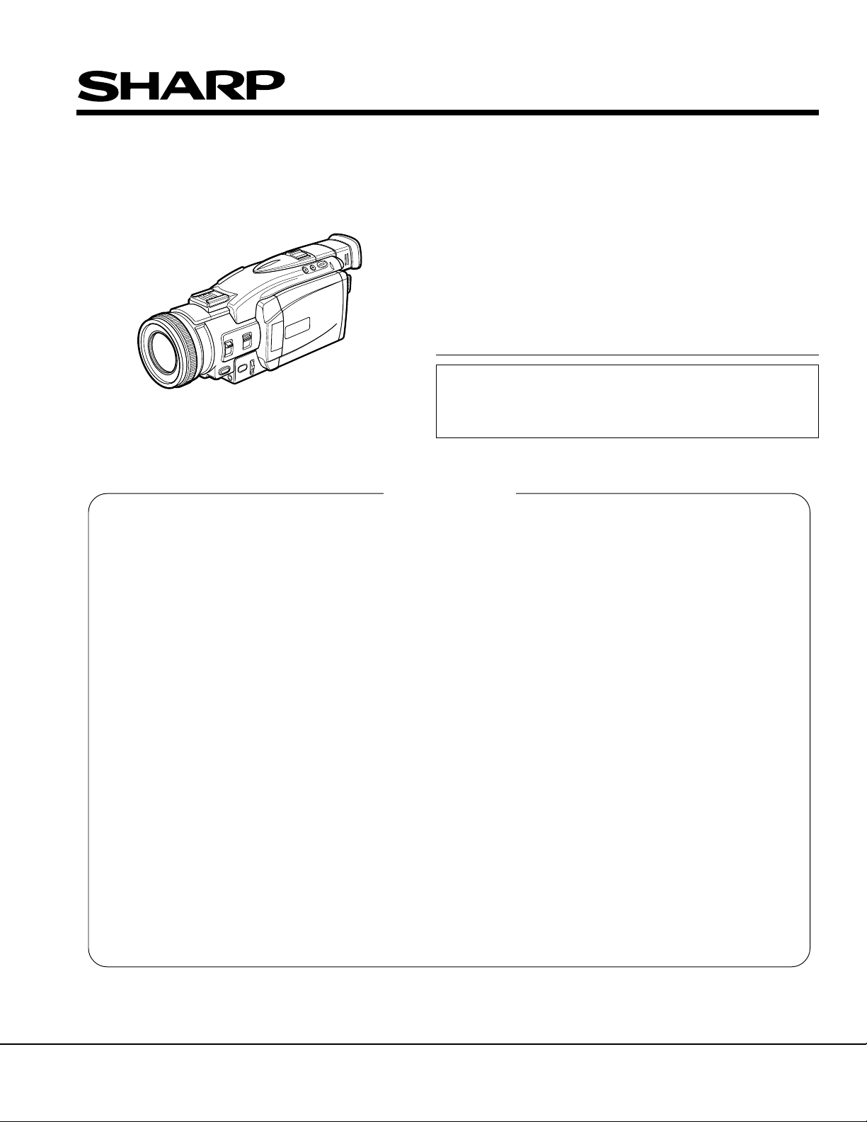
VL-AX1U
SERVICE MANUAL
S52J6VL-AX1U/
LIQUID CRYSTAL DIGITAL CAMCORDER NTSC
LIQUID CRYSTAL DIGITAL CAMCORDER
1. IMPORTANT SERVICE NOTES ........................................................................................................ 2
2. SPECIFICATIONS.............................................................................................................................. 5
3. PART NAMES .................................................................................................................................... 6
4. DISASSEMBLY OF THE SET ............................................................................................................ 7
5. MECHANISM ADJUSTMENT JIGS AND PARTS............................................................................ 10
6. INSPECTION AND MAINTENANCE
ITEMS AND INTERVALS ................................................................................................................. 11
NTSC
MODEL VL-AX1U
7. MECHANICAL ADJUSTMENTS AND CHECKS.............................................................................. 12
8. TAPE RUNNING ADJUSTMENT ..................................................................................................... 15
9. MECHANICAL SECTION ASSEMBLY AND PARTS REPLACEMENT
(DISASSEMBLY AND REASSENBLY) ........................................................................................... 17
10.ADJUSTING THE ELECTRICAL CIRCUITS.................................................................................... 24
11.USEFUL TIPS................................................................................................................................... 45
12.SIGNAL FLOW DIAGRAMS ............................................................................................................. 46
13.BLOCK DIAGRAMS ......................................................................................................................... 49
14.SCHEMATIC DIAGRAMS ................................................................................................................ 56
15.SEMICONDUCTOR LEAD IDENTIFICATION ............................................................................... 110
16.PRINTED WIRING BOARD ASSEMBLIES.................................................................................... 112
17.REPLACEMENT PARTS LIST ....................................................................................................... 123
18.PACKING OF THE SET ................................................................................................................. 145
MODEL
In the interests of user-safety (Required by safety regulations in some countries) the set should be restored to its
original condition and only parts identical to those specified
be used.
CONTENTS
VL-AX1U
Page
SHARP CORPORATION
This document has been published to be used for
after sales service only.
The contents are subject to change without notice.
1
Page 2
VL-AX1U
1. IMPORTANT SERVICE NOTES
BEFORE RETURNING THE VIDEO CAMERA
RECORDER
Before returning the video camera recorder to the user,
perform the following safety checks.
1. Inspect all lead dress to make certain that leads are
not pinched or that hardware is not lodged between
the chassis and other metal parts in the video camera
recorder.
2. Inspect all protective devices such as non-metallic
control knobs, insulating materials, cabinet backs,
adjustment and compartment covers or shields, isolation resistor/capacitor networks, mechanical insulators etc.
3. To be sure that no shock hazard exists, check for
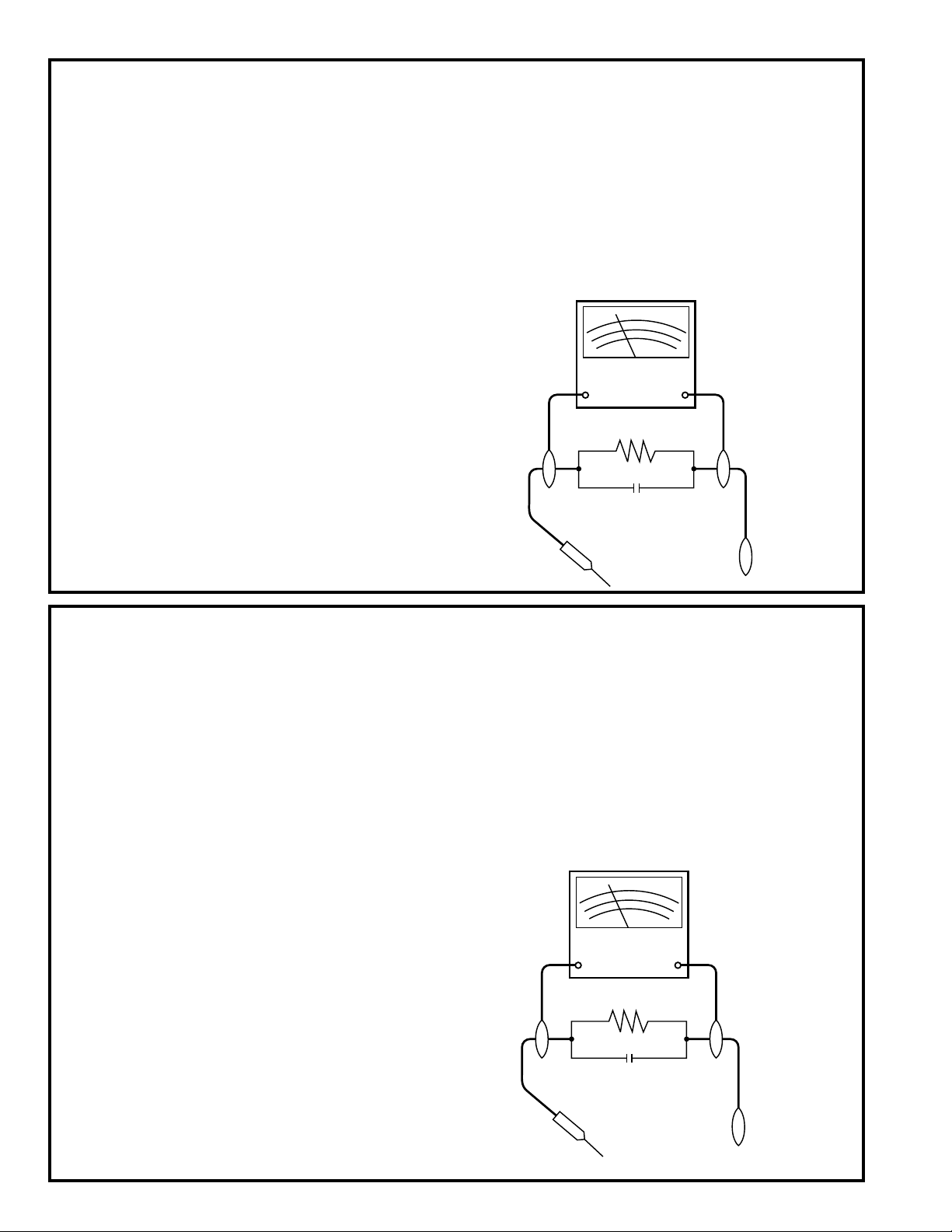
leakage current in the following manner.
· Plug the AC line cord directly into a 120 volt AC outlet
(Do not use an isolation transformer for this test).
· Using two clip leads, connect a l.5k ohm, 10 watt resistor
paralleled by a 0.15µF capacitor in series with all
exposed metal cabinet parts and a known ground,
such as a water pipe or conduit.
· Use a VTVM or VOM with 1000 ohm per volt, or higher
sensitivity or measure the AC voltage drop across the
resistor (See Diagram).
· Move the resistor connection to all exposed metal
parts having a return path to the chassis (antenna
connections, metal cabinet, screw heads, knobs and
control shafts, etc.) and measure the AC voltage drop
across the resistor. Reverse the AC plug (a non
polarized adaptor plug must be used but only for the
purpose of completing these checks) on the set and
repeat the AC voltage measurements for each exposed metallic part. Any reading of 0.45V rms (this
corresponds to 0.3mA rms AC.) or more is excessive
and indicates a potential shock hazard which must be
corrected before returning the video camera recorder
to the user.
VTVM
AC SCALE
1.5k ohms
10W
0.15 µF
TEST PROBE
TO EXPOSED
METAL PARTS
CONNECT TO
KNOWN EARTH
GROUND
1. NOTES DE SERVICE IMPORTANTES
AVANT DE RENDRE LE MAGNETOSCOPE
Avant de rendre le magnétoscope à l’utilisateur, effectuer
les vérifications de sécurité suivantes.
1. Vérifier toutes les gaines de fil pour être sûr que les fils
ne sont pas pincés ou que le matériel n’est pas coincé
entre le châssis et les autres pièces métalliques dans le
magnétoscope.
2. Vérifier tous les dispositifs de protection tels que les
boutons de commande non métalliques, les matériaux
d’isolement, le dos du coffret, les couvercles de
compartiment et ajustement ou les boucliers, les
réseaux de résistance / condensateur d’isolement,
Ies isolateurs mécaniques, etc.
3. Pour être sûr qu’il n’y a aucun risque de choc électrique,
vérifier le courant de fuite de la maniére suivante.
· Brancher le cordon d’alimentation secteur directement
dans une prise de courant de 120 volts. (Ne pas
utiliser de transformateur d’isolement pour cet essai).
· Utiliser deux fils à pinces et connecter une résistance
de 10 watts 1,5 kohm en parallèle avec un
condensateur de 0,15 µF en série avec des pièces du
coffret métallique exposées et une masse de terre
connue telle qu’un tuyau ou un conduit d’eau.
· Utiliser un VTVM ou VOM avec une sensibilité de
1000 ohms par volt ou plus ou mesurer la chute de
tension CA entre la résistance (voir diagramme).
· Déposer la connexion de la résistance à toutes les
pièces métalliques exposées ayant un parcours de
retour au châssis (connexions d’antenne, coffret
métallique, tétes de vis, boutons et arbres de commande,
etc.) et mesurer la chute de tension CA entre la résistance.
Inverser la fiche CA (une fiche intermédiaire non polarisée
doit être utilisée à seule fin de faire ces vérifications.) sur
l’appareil et répéter les mesures de tension CA pour
chaque piéce métallique exposée. Toute lecture de
0,45 V rms (ceci correspond à 0,3 mA rms CA) ou plus
est excessive et signale un danger de choc qui doit être
corrigé avant de rendre le magnétoscope à son
utilisateur.
VTVM
ECHELLE CA
1.5KOHMS
10W
0.15 µF
SONDE D'ESSAI
VERS PIECES
METALLIQUES
EXPOSEES
CONNECTER A
UNE MASSE DE
TERRE CONNUE
2
Page 3
WARNING :TO REDUCE THE RISK OF FIRE OR ELECTRIC SHOCK, DO NO T EXPOSE
THIS APPLIANCE TO WET LOCA TIONS.
CAUTION
RISK OF ELECTRIC SHOCK
DO NOT OPEN
CAUTION: TO REDUCE THE RISK OF ELECTRIC
SHOCK. DO NOT REMOVE COVER. NO
USER·SERVICEABLE PARTS INSIDE.
REFER SERVICING TO QUALIFIED SERVICE
PERSONNEL.
This symbol warns the user of uninsulated
voltage within the unit that can cause dangerous electric shocks.
This symbol alerts the user that there are
important operating and maintenance instructions in the literature accompanying this unit.
CAUTION
This symbol mark means following.
For continued protection against fire hazard, replace only with same type fuse.
(CP1; 1.25A 24V, CP2; 1.25A 24V, CP3;
1.25A 24V, CP4;1.25A 24V)
Camcorder
only
VL-AX1U
ATTENTION:POUR REDUIRE LES RESQUES D'INCENDIE OU DE CHOC ELECTRIQUE,
NE PAS EXPOSER CET APP AREIL A LA PLUIE OU A L'HUMIDITE.
ATTENTION
RISQUE DE CHOC ELECTRIQUE
NE PAS OUVRIR
ATTENTION: AFIN DE REDUIRE LES RISQUES DE
CHOC ELECTRIQUE, NE PAS RETIRER LE
COUVERCLE, AUCUN ORGANE INTERNE
NE PEUT ETRE REPARE PAR
L'UTIUSATEUR, CONFIER L'APPAREIL A
UN DEPANNEUR QUALIFIE.
Ce symbole signale à l'utilisateur la présence
d'une tension non isolée à l'intérieur de l'appareil
qui peut être la cause de secousses électriques
dangereuses.
Ce symbole avertit l'utilisateur que des instructions importantes relatives à l'utilisation
et àl'entretien se trouvent dans le manuel
accompagnant l'appareil.
ATTENTION
Ce symbole signifie que l'on devra utiliser un fusible de même type (CP1;
1,25A 24V, CP2; 1,25A 24V, CP3; 1,25A
24V, CP4;1,25A 24V) pour assurer la
sécurité.
Camcorder
seulement
3
Page 4
VL-AX1U
CAUTION
BEFORE BATTERY DESTROY
NICKEL-CADMIUM BATTERY
The following program is available in the United States. Please consult local environmental
authorities concerning the availability of this or other programs in your area.
The RBRCTM Seal
SHARP participates in the RBRC
States. The RBRC
voluntarily participating in an industry program to collect and recycle these batteries. The RBRC
program provides you with a convenient alternative to placing spent Nickel-Cadmium battery packs into
the trash or municipal waste stream, which is illegal in some areas. At the end of their useful life, the
Nickel-Cadmium battery can be dropped off at the nearest collection center for recycling. For information
on the nearest collection center, call 1-800-8-BATTERY or your local recycling center. If you are located
outside the United States, contact your local authorities for information concerning proper disposal and/
or recycling of this battery. SHARP’s involvement in this program is part of our commitment to protecting
our environment and conserving natural resources.
[Footnote] *RBRCTM is trademark of the Rechargeable Battery Recycling Corporation.
TM Seal on our battery pack contained in our product indicates that SHARP is
TM* Nickel-Cadmium Battery Recycling Program in the United
TM
NICKEL-METAL HYDRIDE BATTERY
LITHIUM or LITHIUM-ION BATTERY
SEALED LEAD BATTERY
Battery disposal
Contains the above (Rechargeable) Battery. must be recycled or disposed of properly.
Remove the Battery from the products and contact Federal or State Environmental Agencies for
information on recycling and disposal options.
4
Page 5

2. SPECIFICATIONS
Signal System: NTSC standard
Recording System: 2 rotary heads, helical scanning system
Cassette: Digital VCR Mini DV video cassette
Recording/Playback Time: 90 minutes (DVM60, LP mode)
Tape Speed: SP mode: 18.812 mm/second
LP mode: 12.555 mm/second
Pickup Device: 1/3.6" (effective size: 5.0 mm) CCD image sensor (with approx. 1,330,000
pixels including optical black)
Lens: 23x optical/500x digital power zoom lens (F1.8-3.5, f = 3.8 – 87.4 mm in
TAPE-CAMERA mode, f = 4.0 – 87.4 mm in CARD-CAMERA mode), fullrange auto focus
Lens Filter Diameter: 46 mm
Monitor: 3.0" (7.5 cm) full-colour LCD screen (TFT active matrix)
Microphone: Electret stereo microphone
Colour Temperature Compensation: Auto white balance with white balance lock and indoor, outdoor, manual ad-
justment feature
Minimum Illumination: 3 lux(with gain-up, F1.8)
Video Output Level: 1.0 Vp-p 75-ohm unbalanced
Audio Output Level: –8 dBs, impedance less than 2.2 kohms
Speaker Output: 300 mW
Still Image Compression System/
Recording Format: JPEG base line conformance/JPEG (Exif2.1)
Still Image Recording Medium: MultiMediaCard, SD Memory Card
Power Requirement: DC 7.4 V
Power Consumption: 4.3 W (during camera recording in TAPE-CAMERA mode using the viewfinder
in Full Auto mode with the DIS function on)
5.1 W (during camera recording in TAPE-CAMERA mode using the LCD monitor in Full Auto mode with the DIS function on and backlight in normal mode)
Operating Temperature: 32°F to 104°F (0°C to +40°C)
Operating Humidity: 30% to 80%
Storage Temperature: –4°F to 140°F (–20°C to +60°C)
Dimensions (approx.): 3 1/32" (W) × 3 3/8" (H) × 8 11/32" (D)
[77 mm (W) x 86 mm (H) x 212 mm (D)]
Weight (approx.): 1.45 lbs(655 g)
(without battery pack, lithium battery, video cassette, lens hood, hand strap
and SD card)
VL-AX1U
AC Adapter/Battery Charger
U ADP-0333TAZZ
Power Requirement: AC 110-220 V, 60 Hz
DC Output: 7.3 V, 1.4A
Power Consumption: 23 W
Dimensions (approx.): 3 5/32" (W) × 1 25/32" (H) × 3 7/8" (D)
[80 mm (W) × 45 mm (H) × 98 mm (D)]
Weight (approx.): 0.43 lbs (196 g)
MultiMediaCard (Supplied Accessory)
Memory Capacity: 8 MB
Power Requirement: 3 V
Operating Temperature: 32°F to 104°F (0°C to +40°C)
Storage Temperature: –4°F to 149°F (–20°C to +65°C)
Specifications are subject to change without notice.
5
Page 6
VL-AX1U
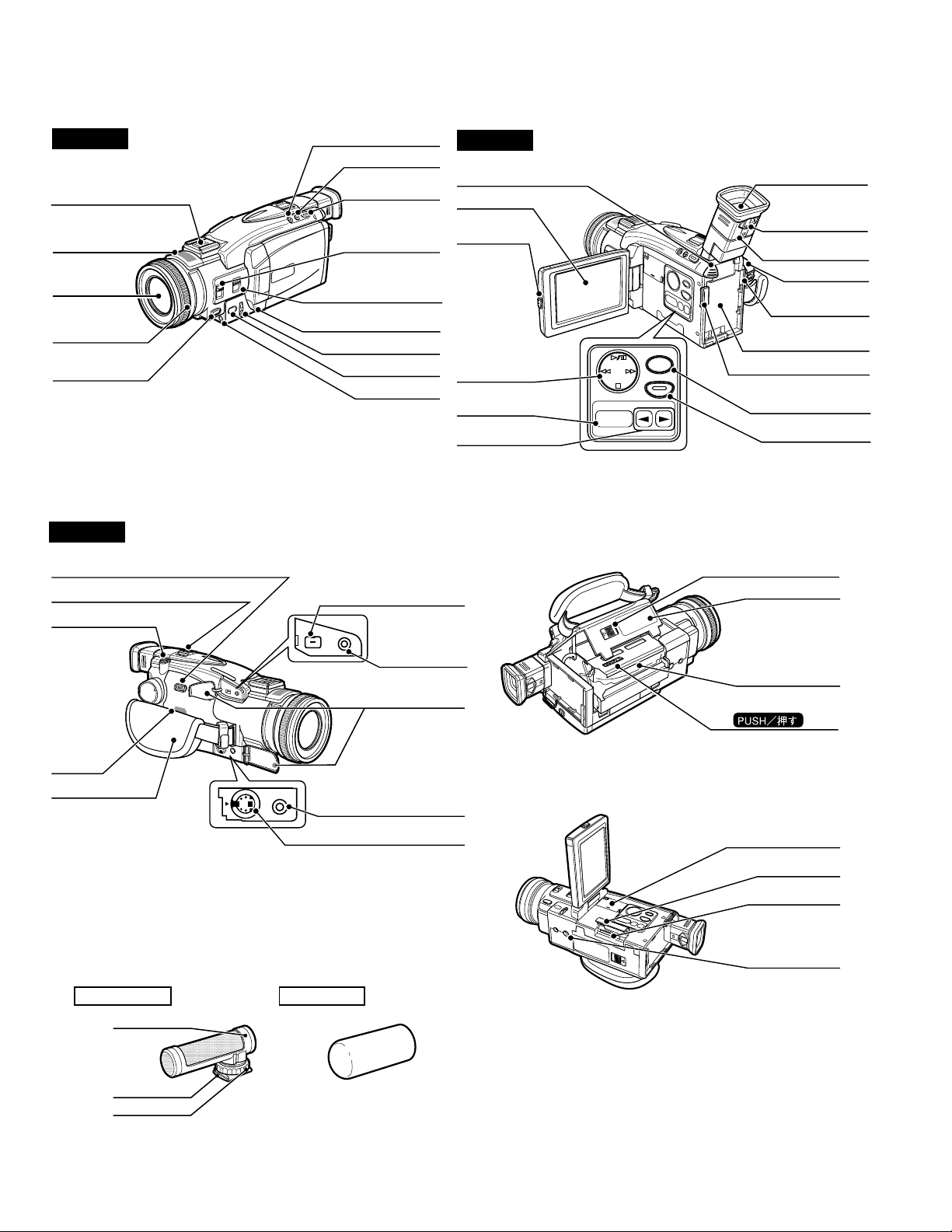
3. PART NAMES
For details on the use of each control.
Front view
Shoe Cover/System Shoe
(to attach zoom microphone)
Built-In Stereo
Microphone
Zoom Lens
Focus Ring
Still Button
Right view
Media Switch
Zoom Lever
Still Button
Volume Adjustment Lever
Stand-by Button
Fade Button
Gamma/Backlight
Button
Focus Switch
Manual Switch
Wireless Remote Control
Sensor
Control Lever
Menu Button
Headphone Jack
DV Jack
(i.LINK)
DV
PC
Communication
Jack
Jack Cover
Left view
Battery Eject Lever
LCD Monitor
LCD Monitor
Unlock Button
Tape Operation
Control Button
Screen Switch
Button
Rewind/Forward
Button
MULTI
DISP. ON/OFF
DIS
Viewfinder
Diopter Scale
Adjustment Knob
Eyepiece Removal
Button
Power Switch
Record Start/
Stop Button
Battery/DC Cable
Compartment
Shoulder Strap Holder
Display On/Off Button
Recording Navigation
Button
Cassette Cover Open Lever
Cassette Cover
Cassette Slot
Cassette Slot
Mark
Speaker
Hand Strap
S-VIDEO
AV
Zoom Microphone Wind Screen
Microphone
Shoe
Shoe Fixer
Video/Audio Jack
S-video Jack
Button Type Battery
Compartment
Card Slot Cover
Card Slot
Tripod Fixing Hole
6
Page 7
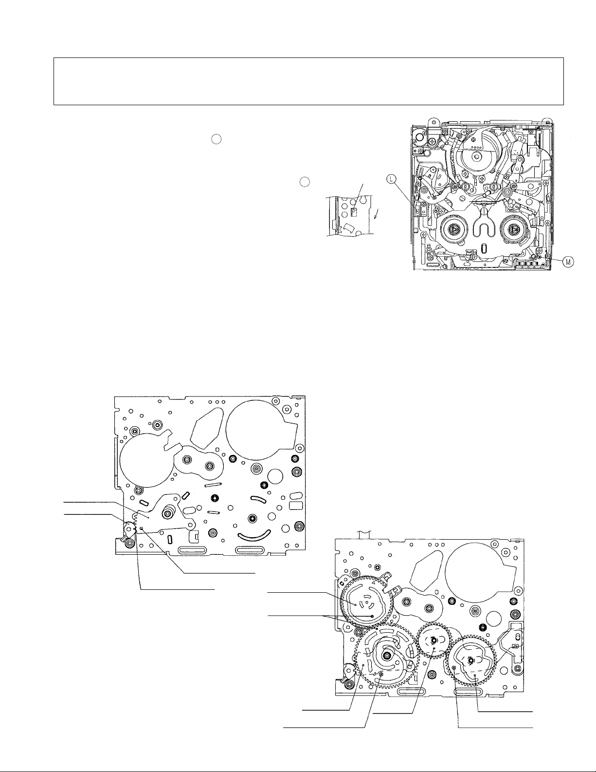
4. DISASSEMBLY OF THE SET
Note:
Before removing the cabinet, turn off the power supply, and ascertain that the battery have been removed.
VL-AX1U
1.
(R)
(O)
Fitting cover
Hot shoe FPC
(P)
Shoe fitting
(S)
(S)
DV·232C unit FPC
(P)
Top cover ass'y
Open the LCD
(P)
• Remove the 1 screw ((O)XiPSF17P03000). Lifting the fitting cover a little, pull it out in the direction of the arrow.
• Remove the 1 screw ((R)XiPSN17P03000), and pull out the shoe fitting in the direction of the arrow.
• Open the LCD, and remove the 3 screws ((P)XiPSF17P04000) and 2 screws ((S)XiPSN17P04000).
Pull out the top cover ass'y in the direction of the arrow to detach the DV•232C unit FPC and hot shoe FPC. (If the top cover
ass'y is pulled out by force, the FPC may be cut off. Therefore, pull it our gently.)
2.
Claw
Tilt FPC
(S)
Operation key unit FPC
(P)
(P)
(K)
Cabinet B ass'y
(O)
(O)
(O)
(O)
(O)
• Detach the operation key unit FPC and Tilt FPC.
• Remove the 1 screw ((S)XiPSN17P04000), 5 screws ((O)XiPSF17P03000), 1 screw ((K)LX-HZ0063TAFN), and 2 screws
((P)XiPSF17P04000).
• Raise the claw in the direction of the arrow, and pull out the cabinet B ass'y to detach the BtoB of the camera operation unit.
(If the cabinet B ass'y is pulled out by force, the FPC may be cut off. Therefore, pull it our gently.)
7
Page 8
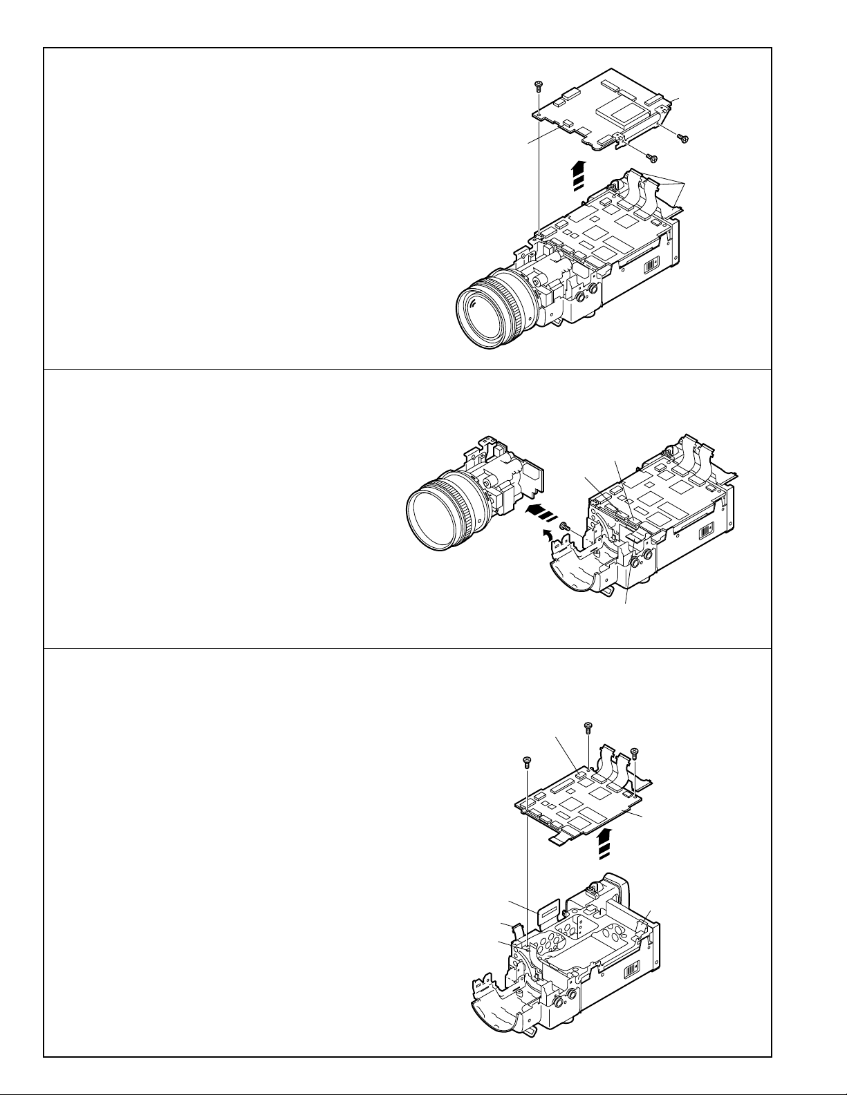
VL-AX1U
3.
• Detach the 3 main=sub FPCs (1, 2 and 3) and 1 microphone
connector.
• Remove the 1 screw ((R)XiPSN17P03000) and 2 screws
((N)XiPSF17P02000), and pull out the sub PWB in the direction of the arrow.
4.
• Detach the lens FPC, focus FPC, and camera=main FPC
BtoB.
• Remove the 1 screw ((R)XiPSN17P03000), raise the claw,
and then pull out the lens section in the direction of the arrow.
Microphone connector
(R)
Sub PWB
(N)
(N)
Main=Sub FPC
Focus FPC
Lens FPC
5.
• Detach the head amp=main FPC BtoB, battery terminal FPC
BtoB, AV/S terminal unit FPC, and power supply S/S unit FPC.
• Remove the 3 screws ((R)XiPSN17P03000).
• Pull out the main PWB in the direction of the arrow to detach
the VF FPC. (If the main PWB is pulled out by force, the FPC
may be cut off. Therefore, pull it our gently.)
Power supply S/S unit FPC
Head amp=Main FPC BtoB
VF FPC
AV/S terminal unit FPC
Claw
(R)
(R)
Camera=Main FPC BtoB
(R)
(R)
Main PWB
Battery terminal FPC BtoB
8
Page 9
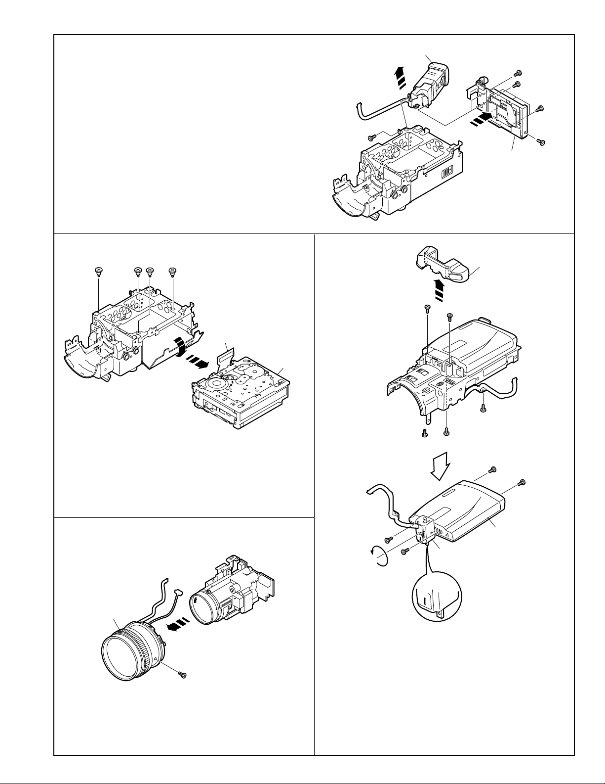
VL-AX1U
6.
• Remove the 1 screw ((Q)XiPSN17P02000) and 5 screws
((O)XiPSF17P03000), and pull out the VF unit in the direction of the arrow.
• Remove the 1 screw ((N)XiPSF17P02000) to detach the
battery cover.
7.
(C)
(B)
(B)
(B)
9.
(Q)
VF unit
(O)
(O)
(O)
(N)
Battery cover
Tilt cover
(F)
(F)
Head-amp=Main FPC
Mechanism
• Remove the 3 screws ((B)LX-BZ0232TAFD) and 1 screw
((C)LX-BZ0245TAFF).
• Open the cassette lid, and pull out the mechanism through the
opening in the direction of the arrow.
8.
Lens cabinet
(R)
(R)
*Hole direction caution
(K)
(O)
(K)
(O)
(O)
LCD cabinet
LCD tilt
(l)
• Remove the 1 screw ((I)LX-HZ0050TAFN), and pull out the
lens cabinet in the direction of the arrow.
• Remove the 2 screws ((K)LX-HZ0063TAFN) and 1 screw
((O)XiPSF17P03000) to detach the tilt cover.
• Remove the 2 screws ((F)LX-HZ0017TAFF) to detach the
LCD cabinet.
• Turn the LCD tilt to verticalize it to the LCD cabinet.
• Remove the 2 screws ((O)XiPSF17P03000) and 2 screws
((R)XiPSN17P03000).
9
Page 10

VL-AX1U
5. MECHANISM ADJUSTMENT JIGS AND PARTS
5-1. Mechanism check adjustment jigs
1. PB-use cassette
Torque meter
2. 9DASD-1015
3. DB
* 1mN·m/1.5mN·m
50 or more
ø2
No. 0 cross-bit
No. 00 cross-bit
1. Torque screwdriver
150mN·m
2. JiGTD1500RTDH
3. CB
1. Torque gauge
2. JiGTG0045
3. CN
For use in VS-REW wind-
*
ing torque measurement.
1. Master plane
2. 9EQMP-VLPD1
3. CL
* For checking reel base
height.
1. Torque gauge head
2. 9EQTGH-DH5000
3. BW
* For use with the torque
gauge listed left.
1. Height adjustment jig
2. 9DAHG-PD1
3. BZ
* For height adjusting.
<Note: The entries of list>
1. Tension gauge 4N
2. JiGSG0400
3. BK
* For measurement of
pinch roller pressure.
1. Height adjustment
screwdriver
2. 9EQDRiVER-DH5
3. BC
*
For guide roller adjustment.
Configuration
1. Name
2. Part No.
3. Code
* Model, Uses Remarks
1. Dial tension gauge
2. 9DAPTG-10-10W
3. CA
* PTG-10
*
For Tu guide adjustment.
*
For T roller adjustment.
*
Bit shape (see figure below).
Tolerance ± 0.1
2
1.4
Tip thickness 0.5
3
<Miscellaneous>
(1) Slide caliper
(2) Precision screwdrivers
1. Alignment tape – ( I )
2. VR3-GAZXS
3. CF
*
For tape running
adjustment.
1. Alignment tape – ( II )
2. VR3-GTZQS
3. CG
*
For SW point adjustment.
* 90ADVC-TAPE can use,
too.
1. For hexagon nut
opposite side 3mm bit.
2. 95CM22001
3. BL
* For S guide hexagon
nut installation.
(Phillips head and slotted)
(3) Radio needle-nose pliers
(4) Tweezers
5-2. Parts for regular periodic inspection and maintenance
1. Oil
Cosmo Hydro HV22
2. 9EQ-Oil-HV22
3. AE
* Cosmo Petroleum K.K.
1. Cleaning paper
2. JiGDUSPER
3. AP
* DUSPER ∑ (SIGMA)
(ozu Co., LTD.)
<How to make jigs for mechanism checking and adjustment>
(1)Reel hub for back tension measurement (Fig. 1)
1) Obtain a commercially available cassette tape reel hub.
(Disassemble the cassette tape and remove the tape from
the reel hub.)
2) Paste one end of a string (about 20cm long) to the reel hub
with (for example) cellophane tape.
3) Paste the weight of about 0.21N on the upper side reel hub.
(2)String for use in pinch roller snap-fit force measurement (Fig. 2)
1) Obtain an approximately 20cm length of commercially available string.
2) Tie the 2 ends together to form a loop.
1. Grease: Moly Coat
YM-103
2. 99FGREASE-YM103
* Dow corning
1. Screw lock (1401B)
* Three Bond
<Note:
The entries of list>
1. Cleaning liquid:
industrial-use ethyl alcohol
* Commercially available item
1. Extremely thin cotton swab
* Commercially available item
Weight
Reel hub
Fig. 1
Configuration
1. Name
2. Part No.
3. Code
* Model, Uses Remarks
String
String
Fig. 2
10
Page 11
VL-AX1U
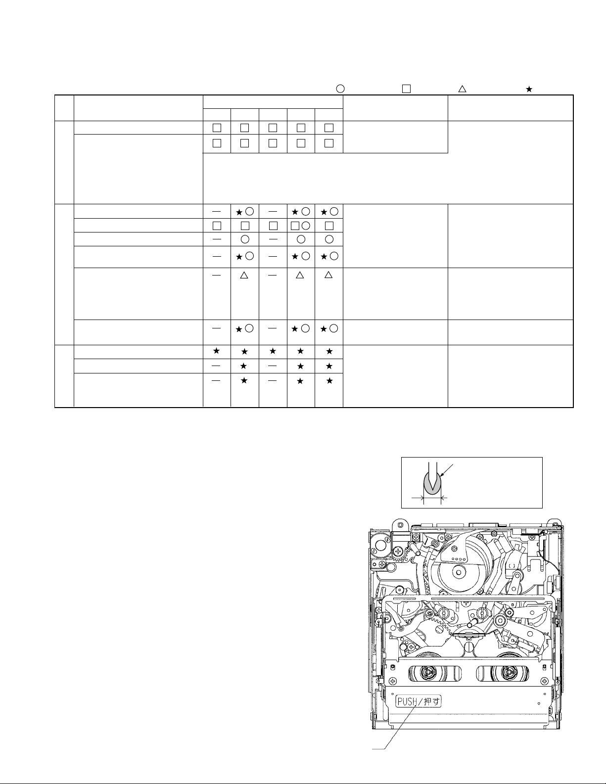
6. INSPECTION AND MAINTENANCE ITEMS AND INTERVALS
In order to keep the mechanical section always in good condition, perform the following inspection and maintenance at regular intervals.
In addition, after repair, perform the following maintenance items regardless of how long the user has been using the unit.
6-1. List of inspection and maintenance items
Inspection and
maintenance location
Tape running section (see section 8-3)
Drum section, Video head
(see section 8-3)
Tape running system
Timing belt
Pinch roller
Capstan motor
Swing arm
S reel base, Tu reel base
Center pulley shaft
Intermediate pulley shaft
Swing arm boss
Drive system
Intermediate gear A shaft,
Intermediate gear B shaft
Loading motor
Mode switch
Abnormal noise
PB · VS/R winding torque
PB · VS/R · loading back tension
Tu reel base ratchet torque
S reel base no-load torque
Performance checks
500 1,000 1,500 2,000 3,000
<Rollers>
• Replace if there is anything abnormal in the rotation, or if there is run-out
(that becomes large).
<Other than the above>
• Clean the section that contacts the tape (especially the lower drum helical
section). Use the specified cleaning liquid.
Time of use (h)
[Oil] Cosmo Hydro HV22
[Grease] Moly Coat YM-103
• • • Replace. • • • Clean. • • • Lubricate. • • • Check.
Symptoms that indicate
need for maintenance
• Block-type noise
• Head hole clogging
• Tape damage
• The tape fails to run.
• The tape becomes slack.
• Block-type noise
• Abnormal noise
• Abnormal noise
• Cannot eject.
• Fails to enter a mode.
• The tape fails to run.
• The tape becomes slack.
• Tape damage
• The play-back image is
abnormal.
[Screw lock] Three Bond 1401B
[Cleaning liquid] Industrial-use ethyl alcohol
Note:
Replace the drum ass'y if the
video head is cleaned but the
envelope still does not appear.
(When the envelope is normal,
refer to "11. USEFUL TIPS".)
• Replace if there is anything
abnormal.
• Lubricate with oil.
[Oil]
Cosmo Hydro HV22
Note:
• Replace if anything is abnormal
(including the noise).
• Replace any part that fails to
perform within the standard.
Remarks
Apply oil to the shaft, then
wipe lightly with a cloth.
6-2. Precautions
(1) When replacing any part, always replace the cut washer that was
removed with a new one.
(2) This mechanism does not have control adjustment. If the control
cannot be set as required, clean and or replace parts.
(3)On the oil
a) Always use the specified oil. (Using another kind of oil can cause
various kinds of trouble.)
b) Always use clean oil, without any mixed-in dirt, to lubricate bearings.
(Using oil with dirt mixed in can cause the bearings to wear or to
stick.)
c) One drop of oil is the amount shown in the Fig. 1, on the point of a
pin.
(4)Perform circuit repair, tape running adjustment, etc. with the cassette
controller assembly attached to the mechanism.
(5) When operating the mechanism separately, apply voltage to the
loading motor. However, the terminal voltage must be DC3V~4V.
(When the mechanism is connected to the main PWB, do not apply
external voltage to the loading motor. It may cause a trouble.)
(Forcing the gears to turn by hand entails danger of breakage.)
If the mechanism is separated from the unit, the capstan motor may rub
and be damaged if spacing under the mechanism is inadequate.
(6)To install the cassette controller, push section A in the Fig. 2. Do not
push anything else.
(7)Do not deform any of the mechanical parts.
Oil
1.5mm diameter or less
Fig. 1
11
A
Fig. 2
Page 12
VL-AX1U
7. MECHANICAL ADJUSTMENTS AND CHECKS
The items discussed here relate to general on-site servicing (field servicing). Adjustments and replacements that require
sophisticated facilities, jigs and technology are omitted.
In addition, in order to maintain the characteristics that the unit has when it is new, not only are inspection and maintenance necessary,
but it is absolutely necessary that, for example, the tape not be damaged, and always use jigs for adjustments that require them.
<Precautions>
(1)Always set the power supply and state of the unit as follows Notes for mechanism adjustments and checks.
AC adapter used, with cassette controller assembly
AC adapter used, without cassette controller assembly (Independent Mechanism)
DC3V, without cassette controller assembly (Independent Mechanism)
(2) When the mechanism is connected to the main PWB, do not apply external voltage to the loading motor. It may cause a trouble.
(3) Always run the tape with the cassette controller assembly attached.
7-1. Checking the playback (recording) winding torque AC adapter used, with cassette controller assembly
(1)Set the torque cassette with the cassette controller assembly attached, then, in SP recording mode (playback mode if a signal has
already been recorded in SP mode on the tape), confirm that the torque on the winding side is within the standard.
<Winding torque standard in record (playback) mode>
(If there is torque ripple, read the center value.)
0.70 +0.4/-0.3mN·m, ripple 0.4mN·m or less
7-2. Checking the rewinding playback (VS-REW) winding torque
AC adapter used, without cassette controller assembly (Independent Mechanism)
(1)Remove the cassette controller assembly, press the DOWN switch, using the
adhesive tape and referring to 9-3, operate in the TEST mode (T01) to rewind,
and set the rewinding playback (VS-REW) mode.
(2)Set the torque gauge on the S reel base, press the front end of tension post with
your finger in the arrow A direction so as to ascertain that the winding torque is
as specified. (Check without rotating the torque gauge.)
<Rewinding playback (VS-REW) winding torque standard>
(If torque ripple exists, read its center value.)
1.6 ± 0.6mN·m, ripple 0.5mN·m or less
(3)After checking the winding torque remove the torque gauge, and remove the
adhesive tape used in item (1) above (refer to 9-3). The STANDBY mode is set
automatically.
Fig. 1. Removal of tension band when
measuring the rewinding playback (VS-REW) winding torque
7-3. Checking of reel base height DC3V, without cassette controller assembly (Independent Mechanism)
(1)Remove the cassette controller assembly (refer to 9-2).
(2)Referring to 9-1, apply DC3V to the loading motor and put the system into playback mode.
(3)Taking adequate care so that the master plane does not contact drum, running parts (guide roller, etc.), or the MIC contacts. Fit
the master plane holes to the 2 guides (A and B) in Fig. 2.
(4)Confirm that the heights of the S reel base reel receiving surface and the Tu reel base reel receiving surface below the master plane
top surface are within the set values, using, for example, a slide calliper (Fig. 3).
When checking the S reel base height, press the front end of tension post in the arrow A direction with your finger to release the
tension band, and then check the height in this state (Fig. 1).
(5)If the height is not within set values, replace the washer under the reel base, and adjust as specified.
Note: After the adjustment, make sure that the reel bases rotate smoothly.
Reel receiving
surfaces
2.4 ± 0.1
2.4 ± 0.1
Reel base height
setting values
Reel base height
Fig. 3
12
A
setting values
MIC contacts
Fig. 2
B
Page 13
VL-AX1U
7-4. Back tension torque check and adjustment in record (playback) mode
AC adapter used, with cassette controller assembly
(1)Checking
Set the torque cassette (SD-1015), and make sure in the SP record mode that
the supply side torque is within the standard shown below (or in the playback
mode for the tape on which the signal has been SP-recorded).
<Standard>
(If torque ripple exists, read its center value.)
0.7 ± 0.1mN·m
(2)Adjustment (Fig. 4)
If the value is out of standard range, adjust, using the screw 1 shown in Fig. 4.
1. Loosen the screw 2 slightly.
2. Adjust to turning the screw 1. When back tension is too high, turn the screw
1 counterclockwise (CCW).
When back tension is too low, turn the screw 1 clockwise (CW).
3. After adjustment fix the angle with the screw 2. (At this time take care so as
to prevent excessive tightening.) Apply Screw Lock to the screw 1.
<Caution>
Screw tightening torque: 0.04N·m
7-5. Checking and adjustment of tension roller position in
record (playback) mode
DC3V, without cassette controller assembly (Independent Mechanism)
(1)Checking
Before winding the 60-min tape make sure that the tension roller is in the same
position as S guide as shown in Fig. 4.
If not, take out the tape and adjust in the following procedure.
(2)Adjustment (Fig. 5)
1. Set the playback mode without loading the tape.
2. Loosen the screw 3 slightly (to such an extent that the tension band holder
4 can be moved).
3. If the tension roller is inside from the specified position, shift the tension
band holder 4 in the arrow
the tension band holder in the arrow
(Proper shift must be 0.2 to 0.6mm outside from the specified position.)
4. Check the position by the procedure described in item (1) Checking above.
5. If the position is not specified position, adjust again.
direction. If the tension roller is outside, shift
A
direction, and fix with the screw 3.
B
Screw1
Apply screwlock
Tension roller position (S guide standard)
0.2~0.6mm (Standard)
Tension roller
Tension roller position (S guide standard)
Screw2
CCW
CW
Fig. 4. Check (tape exists)
0 ± 0.3
S guide
Tension band holder 4
Screw 3
7-6. Checking of supply S reel base no-load torque
DC3V, without cassette controller assembly (Independent Mechanism)
(1)Remove the cassette controller assembly, then apply DC3V to the loading
motor and put the system into L. start mode (refer to 9-1).
(2)Move the swing arm toward the Tu reel base side.
Be careful not to cause damage to the gears and other parts in the process. (Fig.
6)
(3)Set a back tension measurement reel hub on the S reel base.
(4)Using a dial tension gauge, pull the string in the A direction, then confirm that the
tension is within the standard.
<FF back tension standard>
(If the tension fluctuates, read its center value.)
30mN or less
7-7. Checking of loading back tension
DC3V, without cassette controller assembly (Independent Mechanism)
(1)Remove the cassette controller assembly, then apply DC3V to the loading
motor and put the system into L. start mode.
(refer to 9-1)
(2)Move the swing arm toward the S reel base side. Be careful not to cause
damage to the gears and other parts in the process. (Fig. 7)
(3)Set a back tension measurement reel hub on the Tu reel base.
(4)Using a dial tension gauge, pull the string in the A direction, then confirm that
the tension is within the standard.
Fig. 5. Position adjustment
(tape does not exist)
Move the swing arm
A
toward the Tu reel
base side.
Fig. 6. S reel base no-load torque
measurement method
13
Page 14
VL-AX1U
<REW back tension standard>
(If the tension fluctuates, read its center value.)
15 ± 12mN
7-8. Checking of winding Tu reel base ratchet torque
DC3V, without cassette controller assembly (Independent Mechanism)
(1)Remove the cassette controller assembly, then apply DC3V to the loading
motor and put the system into standby mode. (refer to 9-1)
(2)Move the swing arm toward the S reel base side.
Be careful not to cause damage to the gears and other parts in the process.
(Fig. 8)
(3)Set a back tension measurement reel hub on the Tu reel base.
(4)Using a dial tension gauge, pull the string in the A direction, then confirm that
the tension is within the standard.
<Winding Tu reel base ratchet torque standard >
(If the tension fluctuates, read its center value.)
100mN or less
7-9. Checking of rewinding playback (VS-REW) back
tension
DC3V, without cassette controller assembly (Independent Mechanism)
(1)Remove the cassette controller assembly, then apply DC3V to the loading
motor and put the system into rewinding playback (VS-REW) mode. (refer to
9-1)
(2)Move the swing arm toward the S reel base side.
Be careful not to cause damage to the gears and other parts in the process.
(3)Set a torque gauge on the Tu reel base.
(4)Turning the torque gauge to counterclockwise (1 turn for 3 seconds), then
confirm that the torque is within the standard.
<Rewinding playback (VS-REW) back tension standard value>
(If the tension fluctuates, read its center value.)
0.70 +0.6/-0.3mN·m
Move the swing arm
toward the S reel
base side.
A
Fig. 7. Loading back tension measurement
method
7-10. Checking of pinch pressing force
DC3V, without cassette controller assembly (Independent Mechanism)
(1) Set the pinch roller pressing force measuring thread on the pinch lever
(position A , Fig. 9).
(2)Set the mechanism to the playback mode, press the pinch roller against the
capstan shaft.
(3)Fit the tension gauge to the pinch roller pressing force measuring thread, pull
in the arrow B direction shown in Fig. 11 to separate a little the pinch roller from
the capstan shaft.
(4)Gradually return the pinch roller, and when the pinch roller contacts parallel
the capstan shaft, read the value (see Fig. 10) to make sure that the value
conforms to the standard shown below.
<Standard>
1.8 +0.3/-0.5N
<Caution>
After making this measurement, quickly release the system from playback
mode and remove the pinch roller from the capstan shaft. (If the pinch roller
is left fitted onto the capstan shaft for a long time, the pinch roller will be
deformed.)
A
OK
NG
Move the swing arm
toward the S reel
base side.
A
Fig. 8. Winding Tu reel base ratchet torque
measurement method
Pinch roller
Right guide
Capstan shaft
B
Fig. 9
Fig. 10
Fig. 11
14
Page 15
8. TAPE RUNNING ADJUSTMENT
8-1. Adjustment locations
VL-AX1U
<Replacement parts>
· T roller, arm
· Tu guide, arm
· Slide chassis
<Replacement parts other
than those shown above>
· S guide
· Pole base
· Guide roller
· Drum assembly
· Capstan motor, etc.
Adjust the height of only
replaced parts with the
adjusting jig.
Adjustment procedure 8-2
Height presetting is not
necessary.
Cassette controller
installation
Running adjustment preparation
Adjustment
procedure 8-3
Running rough
adjustment
Adjustment
procedure 8-4
Running final
adjustment
Adjustment
procedure 8-5
8-2. Running height adjustment
· After replacement of T roller or Tu guide adjust the height . (Adjust only the replaced parts.)
· After height adjustment do not turn the T roller. If crease is found on the tape of Tu guide, remove the crease by rotating.
(As for details refer to the “Running rough adjustment”.)
· After height adjustment of T roller or Tu guide, apply Screw lock to an end of shaft.
(After replacement of S guide apply Screw lock to same point, too.)
Tu guide
T roller
Height setting
jig
Lower edge
fitting
Master plane
Fit height the par on low edge fitting.
After setting adjustment jigs, turn T roller
counterclockwise to 315°.
Master plane
Height setting
jig
Height setting
jig
Master plane
8-3. Preparation for tape running adjustment
Meters, jig… Oscilloscope, Adjustment remote control, Height adjustment screw driver, Alignment tape (for tape running
adjustment, for switch point adjustment), Master plane, Height adjustment jig.
<Method and description>
(1)Clean the tape running surface (especially, adequately clean
the drum surface and the lower drum helicam surface).
(2)Attach the cassette controller.
(3)Connect an oscilloscope to each TP on the relay circuit board.
(4)Turn the AC adapter power ON.
(5)Using the adjustment remote control unit, put the system TEST
mode T-05.
(6)Replay the alignment tape for running adjustment, and make
sure that the tape is running in the SP mode.
(7)Check the oscilloscope playback envelope, then, at +1/4 shift
and -1/4 shift, check whether all of it is flat. If it is not, perform
the following adjustment so that it becomes flat.
(Each time you push the PLAY key, the shift will change;
+1/4 shift → Normal → -1/4 shift → Normal , in order.)
Sup guide roller
Tension roller
Drum
S guide
Tu guide roller
Tu guide
Pinch roller
Reels
15
Page 16
VL-AX1U
8-4. Running rough adjustment
(With cassette controller)
1) Su, Tu guide roller height adjustment
<Method and description>
(1)Loosen the guide roller lock screw, then tighten loosely so that
the roller turns easily.
(2)Replay an alignment tape, and adjust the Sup, Tu guide roller
so that the envelope sides of entrance and exit are flat.
(3)Perform ± 1/4 shift, then, as in the above case, adjust until the
envelope becomes flat.
* If running is difficult for the entrance changed, turn the T roller
to counterclockwise 180°. (refer to Fig. 1)
2) Check of V/SR envelope wave form
<Method and description>
(1)Confirm that the envelope waveform peaks in V/SR mode are
uniform.
(2) If they are not uniform, fine-adjust the guide roller and the Tu
guide.
3) Check of tape wrinkles
<Method and description>
(1)Check that the tape is not distorted between the Tu guide and
pinch in the PB mode and the V/SR mode.
-If crease is found, make an adjustment in the range of ±180°.
-After adjustment apply Screw Lock.
NG
±1/4 shift ±1/4 shift
Entrance side
Turn to 180°
Exit side
Normal
T roller
Fig. 1
Adjust so that A B.
A
Pinch roller
B
Wrinkles
Tu guide
Deformation
Deformation
NG
•
•
4) Check the rising time of the envelope wave form
<Method and description>
(1)Check the rising time of the envelope when switching from V/SR mode to PB mode. (Within 5 sec)
(2)Check the rising time of the envelope when switching from STOP mode to PB mode. (Within 5 sec)
8-5. Final running adjustment
(With cassette controller)
1) Adjustment of Sup and Tu guide roller height
<Method and description>
(1)Perform ± 1/4 shift, then if the envelope wave's ratio of MAX.
to MIN. are 60% or less, adjust again the height of guide roller.
(Refer to Fig. 2)
(2)Finally adjust the lock screw of Sup and Tu guide roller.
(3)Once perform unloading and then loading to set the PB mode,
and make sure that the envelope waveform does not change.
2) Adjustment of playback SWP
<Method and description>
(1)Playback the alignment tape for switch point adjustment.
(2)Perform SWP automatic adjustment with adjustment remote control.
Fig. 2
* When replacing the mechanism and drum, adjust the phase and equalizer using the adjustment remote control.
(Refer to "10. ADJUSTING THE ELECTRICAL CIRCUITS".)
16
Page 17
VL-AX1U
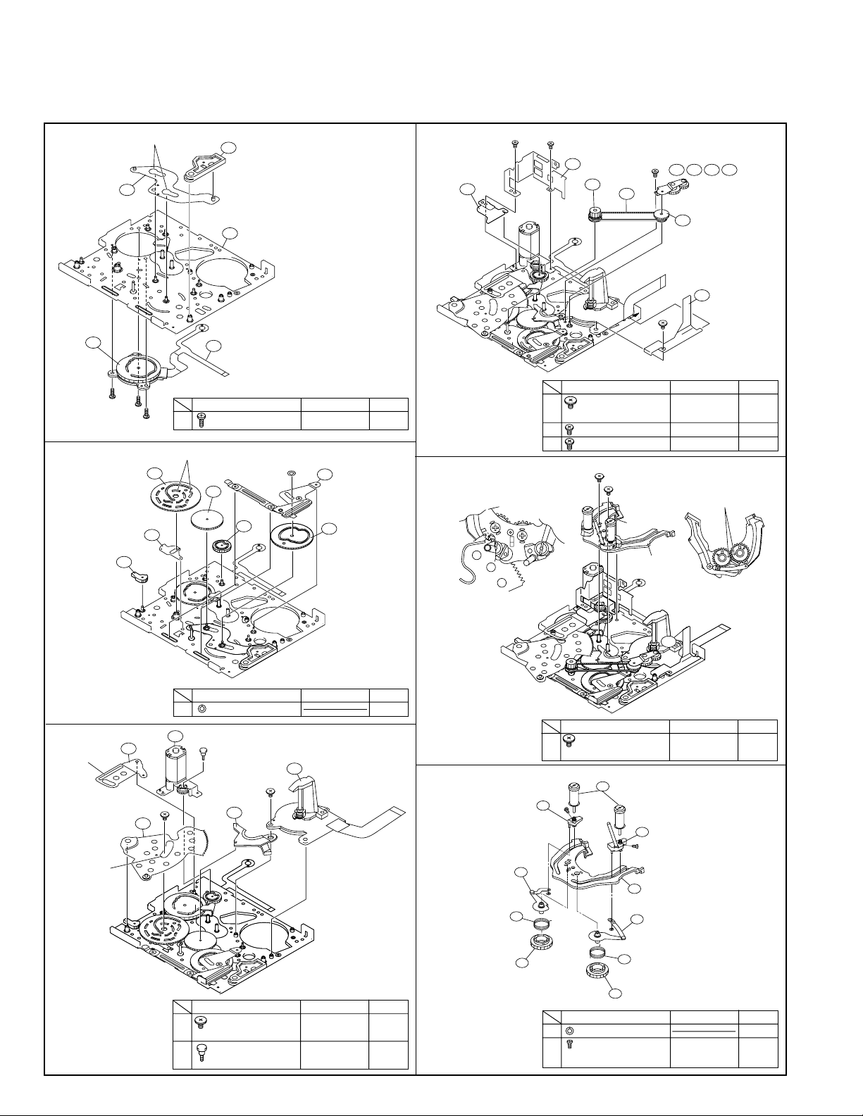
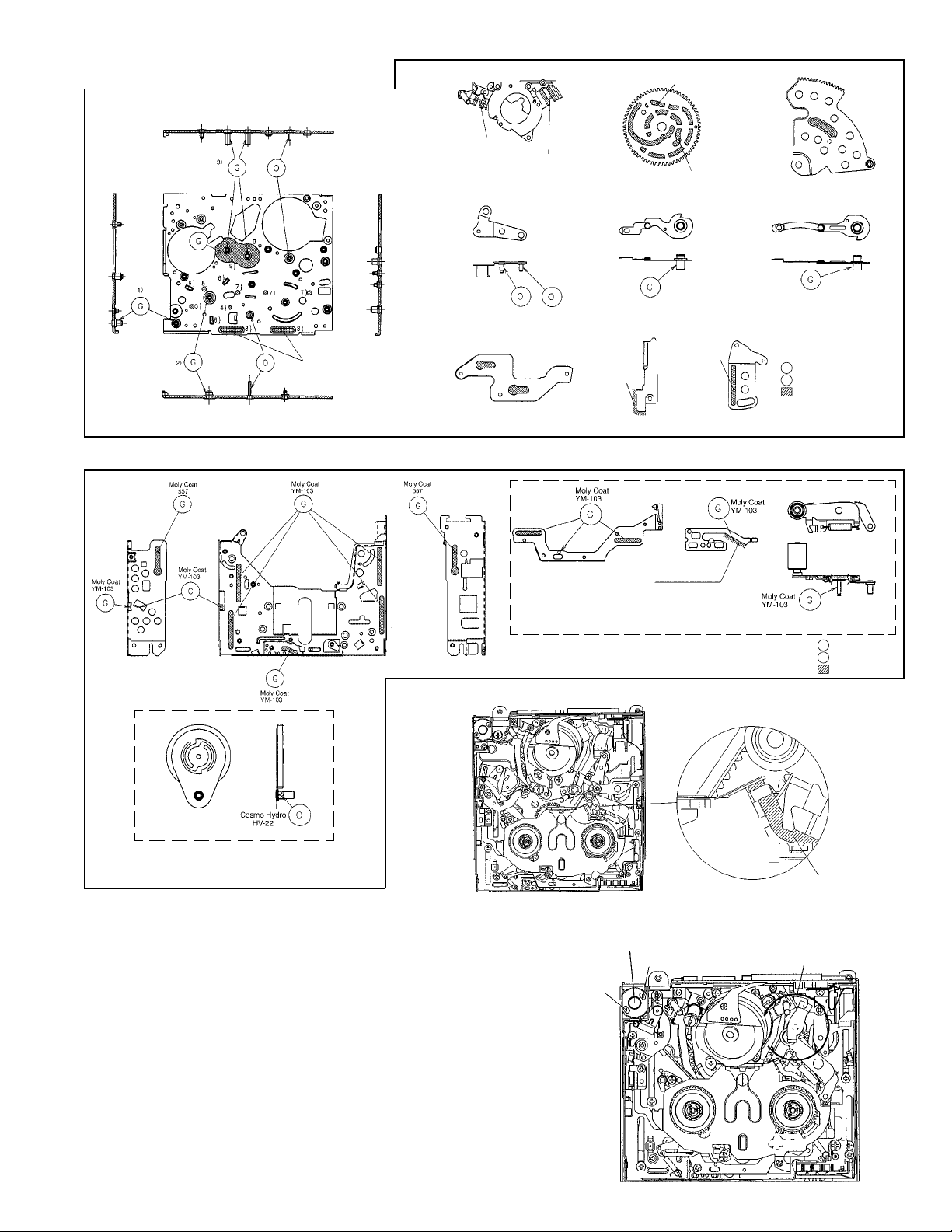
9. MECHANICAL SECTION ASSEMBLY AND PARTS REPLACEMENT
(DISASSEMBLY AND REASSEMBLY)
Mechanical section disassembly and reassembly are explained in this section.
For removal of the cabinet, etc., refer to 4. DISASSEMBLY OF THE SET.
<Precautions>
1. Always replace cut washers that have been removed, for example in parts replacement, with new ones.
When reassembling, be careful not to allow screws, washers or foreign matter to enter. They can cause mechanical misoperation.
2.
3. Use the cleaning liquid, oil, grease and screw lock that are specified below. Use of any other kind can cause mechanical
misoperation.
Oil: Cosmo Petroleum : Cosmo Hydro HV22 Screw lock: Three Bond :1401B
Grease: Dow Corning : Moly Coat YM-103 Cleaning liquid: Industrial-use ethyl alcohol
9-1. On the mechanical modes
When operating the mechanism separately, apply DC3~4V to the loading motor.
(When the mechanism is connected to the main PWB, do not apply external voltage to the loading motor. It may cause operational problems.)
(1)EJECT mode
The mechanism position to take out the cassette where the
EJECT lever is extremely shifted in the A direction. (It is impossible to lock the cassette controller assembly in this mode.)
EJECT lever
A
EJECT mode diagram
(3)LOADING START mode
This is the mode where the tape is wound around the winding
reel when a cassette with visible wind start leader tape is
loaded. (The brake shifter moves to the left, the S main brake
is separated from the S reel base and the Tu main brake is
separated from the Tu reel base.)
(2)STANDBY mode
The mechanism position to set the cassette where the slide
chassis is at the farthest position from the drum and the
EJECT lever is in counterclockwise rotated position (position
where the cassette controller assembly can be locked).
EJECT lever
Rotation
It is hardly seen since
it is concealed with
slide chassis.
Slide chassis
STANDBY mode diagram
(4)REWINDING (VSR) mode
The mechanism position to rewind the tape (fast rewinding
playback). The S and T pole base is pressed, the pinch roller
is pressed to the capstan shaft, the brake shifter VSR brake
section engages with the Tu reel base gear.
T pole base
S pole base
Capstan shaft
Pinch roller
S reel base
S main brake
Brake shifter
LOADING START mode diagram
VSR brake section
Tu reel base
Tu reel base
Tu main brake
REWINDING (VSR) mode diagram
17
Page 18
VL-AX1U
(5)PLAYBACK (RECORD, FF, VSF) mode
The mechanism position for playback, record, FF and fast
feed playback.
The pinch roller is pressed to the capstan shaft, and the S/Tu
main brake is separated from the S/Tu reel base.
Pinch roller
S reel base
S main brake
Capstan shaft
Tu reel base
Tu main brake
(Not visible)
(6)STOP mode
The system is in the STOP (Rec Lock in CAMERA mode)
position; the S and the T pole bases are snap-fitted to the drum
base, the S brake is in contact with the S reel base, and the Tu
brake is in contact with the Tu reel base.
S reel base
S main brake
PLAYBACK mode diagram
(RECORD, FF, VSF)
9-2. Cassette controller assembly
<Removing>
(1) Apply DC3V to the loading motor to enter the standby mode.
Press the lock lever in the arrow direction to raise the cassette controller. (See Fig. 1;
(2) Turn the damper lever in the arrow
(3) Remove two screws
, and remove the down guide D in the arrow
E
Take care that the slide chassis is provided with the down guide positioning G or
(4) Slide the cassette controller in the arrow
and turn the cassette controller in the arrow
(5) Slide the cassette controller in the arrow
direction to release the engagement of the damper bar. (See Fig. 2.)
C
direction, remove the outer link shaft (both sides) toward the inside of the mechanism,
I
direction. (See Fig. 5.)
J
direction. (See Fig. 6.)
K
direction. (See Figs. 3 and 4.)
F
S pole base
T pole base
STOP mode diagram
or B direction.)
A
.
H
Tu reel base
Tu main brake
<Installing>
(1) Apply DC3V to the loading motor to enter the standby mode.
(2) For assembly, reverse the removing procedure (5) thru (2).
Tightening torque of two screws E: 40±4mN.m
Fig. 1.
Fig. 3.
Fig. 2.
Fig. 4.
Fig. 5.
Fig. 6.
18
Page 19
VL-AX1U
9-3. How to operate with the circuit board without the cassette controller assembly.
In this method, if the procedure is followed incorrectly there is danger of damaging the mechanism and the tape, so except in special
cases, such as when measuring the VSR torque, do not perform this procedure. Normally operate this unit with the cassette controller
assembly attached.
Be sure to follow each caution mentioned.
(1) Apply DC3 ~ 4V to the loading motor to enter the standby mode.
(2) Securely press the movable piece
cellophane tape or similar to turn on SW. (Take care that the
movable piece turns only in the shown arrow direction.)
Note: To enter REC mode, press the pin of the recognition switch
(Unnecessary in other modes.)
(3) Set the test mode (T-01) with the adjustment remote controller
without putting the tape, and the mechanical operation will
become possible with the mode key.
(4) For ejection, remove the tape of (2).
of the down SW with
L
Movable piece
.
M
of down SW.
Side view
Rotary direction of
movable
piece
9-4. Phase matching
Fig. 7. LOADING START mode
Referring to Figs. 8 and 9, align the phase for the following parts.
(1) Eject lever (2) Eject control lever (3) Mode SW (4) Main cam (5) Sub cam
Note: Before disassembly, sufficiently check the marker position.
Note: When installing the joining gears, verify that the phase matching holes of the main cam and subcam are aligned to the hole of
the chassis.
Note: After the phase is aligned, turn the mode SW with hand, and verify that it turns nearly one turn.
(After verification, return it to the original position.)
Eject
control lever
Eject lever
Phase matching hole
(for chassis)
Phase matching hole
(for gear)
Fig. 8
Mode switch
Phase matching
mark
Main cam
Phase matching hole
(for chassis)
19
Coupling
gear
Fig. 9
Sub cam
Phase matching hole
(for chassis)
Page 20
VL-AX1U
9-5. Reassembly
9-5-1. Reassembly in side of the main chassis.
Note) Numbers before part names are given as a guide to the order of assembly.
As for greasing/oiling/cleaning places refer to the attached drawings (Grease/Oil application side of the main chassis).
1.
Pinch control lever
Mode SW
463
Groove grease
303
Pinch drive lever
361
Main chassis Ass'y(Front surface)
301
LM/Mode FPC
465
4.
T arm control
lever stopper
363
E
E
H/A PWB angle
315
Center pulley
Ass'y
Drive belt
367
459
Intermediate gear angle
sub Ass'y
F
312
364
366
Intermediate pulley
Ass'y
Capstan FPC stopper
311
C
365
421
Intermediate gear
stopper
2.
3.
Groove grease
A-3
EJECT control lever
EJECT lever
T arm control lever
Loading lever
Groove grease
360
309
A-2
A-1
Main cam
302
306
Item
Tightening torque
A S Tight · M1.4 x L3 70mN·m3
Cam groove grease
304
Coupling
gear
370
AHC cam
369
Item
Shifter drive lever
B
305
371
Sub cam
Tightening torque
BCWø1.2-ø3.0-t0.25 1
Loading motor Ass'y
461
D
Loading motor
fitting Ass'y
Slide chassis
C
guide
Capstan motor
462
C
386
Quantity
Ass'y
Quantity
5.
6.
Phase match check
Sup pole base Ass'y
S loading arm
Ass'y
S pressure spring
Item
Tightening torque
C Special screw · 40mN·m1
M1.4 x L1.6
E S Tight · M1.4 x L4 70mN·m2
F S Tight · M1.4 x L2 70mN·m1
G
G
Phase match check
Guide rail sub Ass'y
(Rear surface)
Tightening torque
40mN·m2
G
Special head screw ·
Enter part of
convexity rear
surfacer
Guide rail sub Ass'y
Item
M1.4 x L1.5
Guide roller Ass'y
454
I
451
Tu pole base
452
Ass'y
I
307
Guide rail
H
395
362
Tu loading arm Ass'y
308
H
Quantity
Quantity
Item
Tightening torque
Quantity
C Special screw · 40mN·m2
M1.4 x L1.6
Special screw with step
D
· 70mN·m1
M1.4 x L6.25
20
372
S loading gear
Tu pressure spring
396
373
Tu loading gear
Item
Tightening torque
Quantity
HCWø0.7-ø2.2-t0.25 2
I Special screw · 5mN·m2
M1.2 x L1.8
(Tentative tightening)
Page 21
9-5-2. Reassembly in side of the Slide chassis.
Note) Numbers before part names are given as a guide to the order of assembly.
As for greasing/oiling/cleaning places refer to the attached drawings (Grease/Oil application side of the slide chassis)
VL-AX1U
1.
S cassette stay
Note1)
Slide adjustment
angle
344
Grease
376
Sensor FPC cover
502
K
382
Tu pole
381
383
352
Tu guide
Ass'y
arm
393
Tu guide
arm SPR.
Tightening torque
397
Guide
adjustment
SPR.
H
Quantity
466
Damper
Spring
J
F
Grease
353
Brake shifter
Ass'y
331
Slide chassis Ass'y
Item
T roller upper
flange
T roller bottom
flange
F S Tight · M1.4 x L2 40mN·m1
HCWø0.7-ø2.2-t0.25 1
J Special screw · 40mN·m1
M1.2 x L1
Note 1: Use the No. 00 bit.
K
Special head screw ·
40mN·m1
M1.4 x L2
2.
T roller upper
382
flange
455
Tension arm Ass'y
3
54
456
N
T spring
hanging
ANG
356
K
B
Tu main
brake
375
O
411
415
M
T arm SPR.
392
H
N
391
Main brake
SPR.
351
Tu reel base
Ass'y
457
411
O
Main brake SPR.
Fit the main brake SPR from
above, and close with the hook.
Swing arm release
lever fixing screw
Swing arm
release lever
Swing arm
release SPR.
420
357
390
Tension band
Ass'y
S reel base Ass'y
S main brake
374
391
F
L
Note 1: Take care for scratch and hit mark on 381, 382 , 383 , 384 and
455 . Handle the tension band with care against deformation.
Note 2: After lightly tightening 428 arm area against deformation,
apply screw-lock on the tip of the shaft.
3
84
383
397
Guide adjustment
SPR.
S guide hexagon nut
428
385
S guide sleeve
415
Pinch lever Ass'y
458
Pinch lever
394
return SPR.
H
T roller Ass'y
T roller inner
T roller bottom
flange
Grease
Item
Tightening torque
Quantity
BCWø1.2-ø3.0-t0.25 1
F S Tight · M1.4 x L2 40mN·m1
HCWø0.7-ø2.2-t0.25 2
Special head screw ·
K
40mN·m1
M1.4 x L2
Special screw with step
L
· 40mN·m1
M1.4 x L1
Type 2 minuteness
M
40mN·m1
M1.4 x L1
NCWø0.7-ø1.8-t0.1 2
OWø1.2-ø2.5-t0.3 2
21
Page 22
VL-AX1U
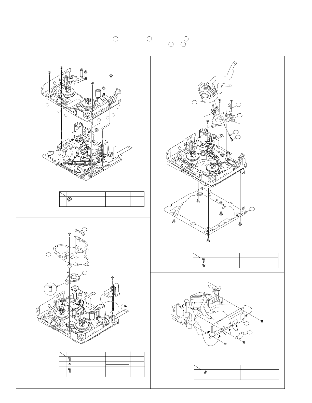
9-5-3. Main chassis assembly and slide chassis assembly assembling method
(1)Enter the coupling mode. (In this position, the cam groove of the T arm operation lever in the figure is parallel to the side of the main
chassis, and the poll base is slightly moved.)
(2)Insert the slide chassis side operation pins (1 tension arm, 2 Tu guide arm, 3 pinch lever) in the position shown below at the
A
main chassis side, move the slide chassis in the arrow direction, using
into the groove of slide chassis, and install with the 4 screws.
to D as guides, insert the loading lever operation pin
1.
C
C
C
B
A
1
D
Item
C
Special screw ·
C
C
2
3
Tightening torque
40mN·m4
Quantity
M1.4 x L1.6
2.
FPC cover
377
P
3.
A
A
399
PB guide SPR.
453
Drum base Ass'y
Grease
(Front surface, rear surface,
groove side surface)
Drum fixing SPR
398
Drum installation screw
438
Tightening torque
50mN·m
Mechanism fixing angle
314
F-4
F-3
F-2
470
Drum Ass'y
Grease
(Rear surface,
groove side surface)
F-5
A
355
Reel cover Ass'y
Oil
Swing arm Ass'y
N
313
Item
A
Tightening torque
Quantity
A S Tight · M1.4 x L3 40mN·m1
NCWø0.7-ø1.8-t0.1 1
Type 1 minuteness
P
40mN·m1
M1.4 x L1
F-1
Item
Tightening torque
Quantity
A S Tight · M1.4 x L3 70mN·m3
F S Tight · M1.4 x L2 70mN·m5
4.
Q
Quantity
Q
Q
Item
Special screw ·
M1.4 x L2
500
Head amplifier PWB unit
501
H/A FPC shield plate
Q
Tightening torque
40mN·m3
22
Page 23
VL-AX1U
GREASE/OIL APPLICATION
Including groove
side surface
(Applied)
Rear surface · groove
side surface
Drum base assembly
Intermediate gear angle
Pinch control lever
Front surface · rear
surface · groove
side surface
Side of the main chassis
(Applied)
Main cam
S loading arm
Enabled after
Enabled after
assembling
Capstan FPC stopper
assembling
From rear
surface side
From rear
surface side
T arm control lever
Loading lever
Tu loading arm
: Oiling(Cosmo Hydro HV22)
O
: Greasing(Moly Coat YM-103)
G
: Greasing(Moly Coat YM-103)
Swing arm
After joining the main chassis
and slide chassis
9-6. Removing the cassette
(1)Apply DC3V to the loading motor unload slightly.
(2)After the tape is slackened, turn the rotor (lower side of mechanism)
of capstan motor to tighten the tape. (Arrow direction, Fig. 1)
(3) Repeat the operations (1) and (2). After the pole base has been
completely unloaded, ascertain that the tape is not loose.
(4)Finally apply again DC3V to the loading motor, so that the cassette
controller ejects.
(5)Take out the cassette.
Note) DC3V is applied to the loading motor as shown Fig 1. Then, the
mechanism moves in the unloading direction.
Enabled after
Brake shifter
assembling
Slide adjustment angle
Side of the slide chassis
Sensor FPC wiring
Loading motor
Minus pole
Plus pole
Pinch lever
: Oiling
O
: Greasing
G
: Greasing
Part A
Capstan motor rotor rotation direction
(from rear side of mechanism)
Sensor FPC
23
Fig. 1
Page 24

VL-AX1U
10. ADJUSTING THE ELECTRICAL CIRCUITS
Before starting the electric circuit adjustment
• The adjustment methods described herein are used, in most cases, when the expendable mechanical parts, including
the video head, have been replaced, at which time the electrical circuits need to be readjusted. Before adjusting the
electrical circuits, make sure that the mechanism works properly (i.e., the mechanism is properly adjusted). Incase of
the occurrence of any problem to the electrical circuits, be sure to use the specified measuring instruments to locate
the area to which the problem is occurring, and then take the necessary action, including repair, replacement or
adjustment, exactly as instructed in the electrical adjustment methods that will follow.
Do not attempt to make adjustments without using the proper measuring instruments.
• This machine is configured so that the electrical circuits inside its PWB unit are composed, for the most part, of highdensity, small surface-mounted component parts for downsized machine body.
To perform repair service or parts replacement, do so using a soldering iron, but in as short a time as possible; this is
because surface-mounted component parts are generally so small in size and susceptible to heat, as compared with
the large discrete parts used in TV sets, desk-top video decks, etc., that attempting to heat their electrodes for a longer
time than is necessary with a soldering iron may result in their becoming defective.
This applies particularly when replacing the laminated chip capacitors.
For this purpose, ceramic soldering irons with a temperature regulator are recommended (iron tip temperature 250°C
and soldering time 5 seconds or shorter).
VL-AX1U Specifications of service jigs
No. Connection section Connector REF. No.
1 H/A PWB–H/A FPC P306 80B-B C QCNW-1832TAZZ BV
2 H/A FPC–MAIN SC3301 80B-B CPWBH2925TA01 Product unit use AR
3 MAIN PWB–SUB PWB SC5701, SC5702 39P QPWBH3224TAZZ Product unit use AE
4 MAIN PWB–SUB PWB SC5703 45P QPWBH3225TAZZ Product unit use AF
5 Power SW–MAIN PWB SC703 17P QSW-Z0370TAZZ Product unit use AR
6 V/F–MAIN PWB SC8801 21P DCOVA1793TAK1 Product unit use AS
7 DV/232C/ZOOM SW– SC5704 21P RUNTK0411TAZZ Product unit use AT
MAIN PWB
8 AVS/EJECT SW– SC1401 21P RUNTK0409TAZZ Product unit use AT
MAIN PWB
9 Hot shoe–SUB PWB SC6602 12P QPWBH3227TAZZ Product unit use AG
10 Battery Terminal– SC900 20B-B QTANZ0149TAZZ Product unit use AQ
MAIN PWB
11 VCR operation–SUB PWB SC3707 10P QSW-ZA002WJZZ Product unit use AV
12 Focus Ring Unit– SC701 10P RUNTK0410TAZZ Product unit use AQ
MAIN PWB
13 Camera Operation FPC– SC3702 30B-B N QCNW-2067TAZZ BS
SUB PWB
14 Camera Operation FPC– 30B-B QSW-Z0371TAZZ Product unit use AZ
Camera Operation Unit
15 CAMCCD PWB– SC1002 39P CPWBH3087TA01 Product unit use AL
CAMCCD FPC
16 CAMCCD FPC– SC201 40B-B C QCNW-2001TAZZ BY
MAIN PWB
17 LCD PWB–MAIN PWB SC2801 33P QSW-Z0372TAZZ Product unit use AT
18
TP Jig for Envelope confirmation
19 Built-in microphone– P6601 4P RMiCC0106TAZZ Product unit use AQ
SUB PWB
SC3703 14B-B N RUNTK0414TAZZ BA
No. of pins
New or
Continuation
Part cord
Price
code
24
Page 25
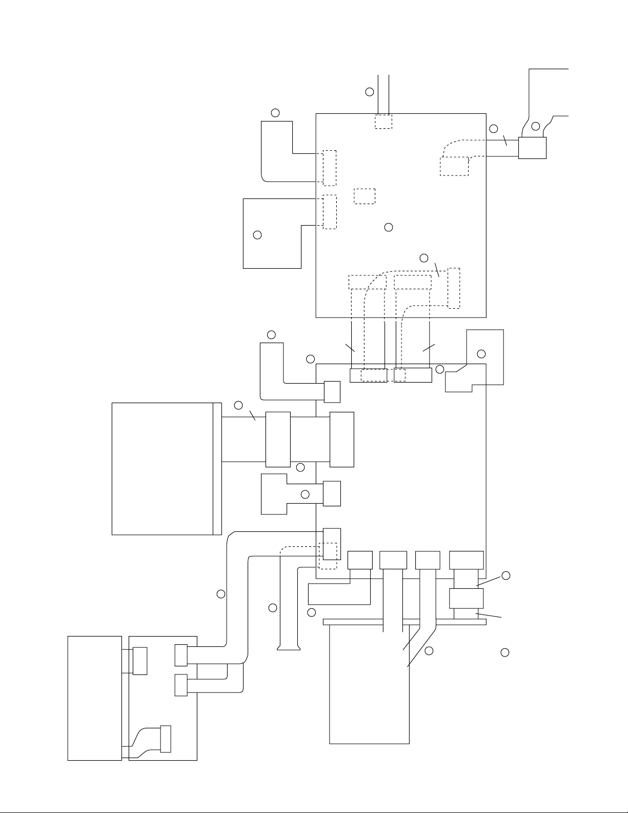
VL-AX1U Service jig configuration
3
3
4
2
1
7
16
12
Hot Shoe
Sheet Key
QCNW-2067TAZZ
<Sub PWB>
45p
39p
39p
39p
39p
45p
BT
POW/SS
QCNW-1832TAZZ
H/A Unit RAMP-0035TAN0
Mechanism
DMECV0067GE71
DV/232C/
ZOOM
AVS/
EJECT
Lens
<Main PWB>
QCNW-2001TAZZ
RUNTK
0409
TAZZ
Lens
V/F
V/F
LCD
<LCD PWB>
BL
Panel
Panel
DMON-0011QA01
Product unit use
RUNTK0411TAZZ
Adjustment Connector
10
13
14
5
11
9
18
17
6
8
19
15
Product unit use
DCOVA1793TAK1
Product unit use
QSW-Z0372TAZZ
Product unit use
Product unit use
(Lens Ass'y)
Product unit use
CPWBH2925
TA01
to Mechanisim
Product unit use
RUNTK0410TAZZ
Product unit use
QPWBH3224
TAZZ
Product unit use
QPWBH3224
TAZZ
Product unit use
QTANZ0149TAZZ
Product unit use
CPWBH3087TA01
Product unit use
QPWBH3225TAZZ
Product unit use
QSW-Z0370TAZZ
Product unit use
QSW-ZA002WJZZ
Product unit use
QPWBH3227TAZZ
Product unit use
QSW-Z0371
TAZZ
Product unit use
RMiCC0106TAZZ
<Camera PWB>
RUNTK0414TAZZ
(TP Jig for Envelope confirmation)
Camera Operation
Microphone
Camera
Focus
VL-AX1U
25
Page 26
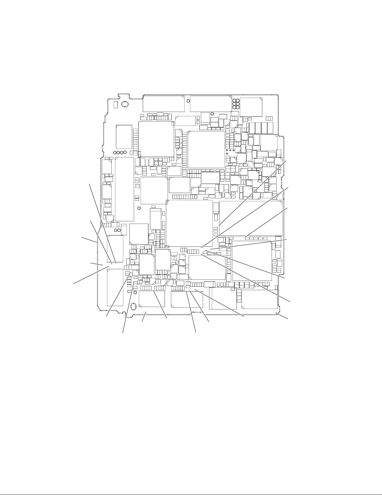
VL-AX1U
[TEST POINT]
(Wiring board diagram: Main Side B)
TL8843(VB)
VF sub-brightness R/B
TL8841(VG)
VF COM-DC
VF brightness
VF contrast
VFγ1
VF sub-brightness R/B
TL8861(BLD)
VF VCO
TL8840
VF COM-DC
TL8842(VR)
VF sub-brightness R/B
TL2804(VGL)
COMMON PULSE
R3493R3492
IC3405
C3462
R3491
R3495
C450
R440
R441
IC405
R442
C452
R443
R446
C451
C407
R411
R406
Q1947
R1992
C404
R407
R412
C405
R416
TL3320
TL8855
TL8861
TL783
SC5704
TL5760
TL5758
TL8840TL8842TL8841TL8843
TL911
TL2811
TL2813
TL2814
TL2818
TL2819
SC2801
TL2825
TL1913
TL1909
TL2834
TL2803
COMMON PULSE
TL5769
TL5766
TL5762
TL5755
TL787
TL785
SC703
TL3332
SC3301
TL403
C508
TL416
TL417
TL4436
TL5768
TL5756
TL5761
TL5759
R2833
R2814
R2811
TL2812
C2808
R2825
R2823
TL2817
R2822
TL2816
TL2815
TL2820
TL2833
TL5763
TL5765
TL5757
TL3406
TL3403
TL3401
C1720
C1718
C1717
C1714
R1711
R1710
C1712
C1710
R1709
R1708
R1707
R798
R1704
C1708
R1726
R1717
R1701
R1721
R1720
TL3321
R2592
C2548
R2582
R2583 R2584
R2588 R2585
Q2510
R2832
C2805
R2812
C2807
D2801
R2815
TL2804
Q2800
R2813
R2810
TL2803
R2831
R2818
R2820
R2819
R2824
TL1908
TL1475
PCO D/A-Y
TL5754
TL5764
R5701
C1724
C1704
TL913
L1702
R1724
R1719
R1718
Q1701
R1723
IC503
R2589
R2594
C2542
R2581
R2617
R2605
C2551
R2616
R2615
C2552
R1470
FB1472
SC1401
TL1475TL1478 TL1481TL1479
R1948
R1713
C1728
TL5776
R2516
R2512
R2586
R2587
R2590
C2546
R2593
IC2507
R2610
R2606
R2604
R2623
R1471
R1476
R1950
R1716
C1725
R1714
IC1701
R1705
C1703
R1702
C1711
TL5772
C4701
IC4701
C4702
FL501
R520
R519
R516
R518
Q504
R517
R537
R2509
R2514
R2511
C2516
C2549
C2544
D2504
TL1480
TL1477
R1475
R1472
SC5701
C1721
R1949
R1715
C1726
C1727
C1723
R1706
C1709
C1702
C1701
R1703
C722
R749
L1701
C724
R754
TL5767
R514 C504 R531
C513
C515
C516
C514
C2515
C2512 R2507
R2515 R2508
IC2502
R2526
R2528
R2529
R2530 R2521
C2517 C2518
C2520 R2520
D2501 R2519 R2522
R1473
R1474
R1477
FB1471
TL1477
PCO D/A-C
0
TL789
TL788
TL3331TL3330TL3329
TL3322
TL5750
TL5753
TL5775
TL5777
TL5773
TL910
TL1914
C1719
C1722
TL1910
IC705
R1722
TL5784
TL5771
TL5785
R706
Q1940
R710
R708
R1712
R733
C1716
R740
C1715
R730
R776
C1713
C734 R770
R774
R781
R757
R713
R711
R716
R782
C1705
C1706
C1707
R719
Q702 Q701
C729
C728
R752
C723
IC706
R753
C726
C506
IC502
TL5770
C512
R535
C502
C511
R536
C503
IC501
TL5789
TL5790
TL5788
R521
R522
R523
TL5786
C2513
TL5752
Q2502
R2510
R2513
TL5778
Q2504
R2534
R2533
Q2507
Q2503
Q2508
C2511
R2527 R2525
L2502
R2537
Q2501
C2503
TL2801
TL2800
C2553
C2554
R2518
R2524
R2523
R2517
SC5702
TL5783
TL5751
TL3319
C934
C936
C721 R755
L903
TL5779
L902
TL5782
C733
C732
TL5774
C718 R744
IC704
C720 C730
R746
R748
R751 C737
C725 R758
R779 R750
R703 R718
C727 R756
C719 R704
X702
IC708
TL797
TL776
TL799
C702
Q703
IC701
C701
TL5780
TL4403
TL7801
IC2501
C2508
R2502
D1900
R780
R506
C230
FB201
TL4440
TL7800
R509
C507
R526
TL4404
R2503
C2501 C2510
R2505
C2507
R2504
TL5781
R505
R504
C509
R532
R533
TL4405
C2555
C2556
R2538
C2530
C2531
R2532
C2504
C2502
R2501
C2506
C2505
TL2802
SC2501
TL2801(G OUT)
DAC full-scale
TL2800(R OUT)
C935
L904
C716
C709
C712
L701
C202
C501
L501
R796
R2506
SC701
TL1904
TL1905
Q1908
R1925
R735
R729
C731
R736
R738
C735
R747
R723
TL420
TL418
TL412
TL5787
R734
R737
R769
R772
TL914
R761
R763
R764
C711
C706
Q1920
R1911
FB203
C224
R205
TL912
C222
C5702
C5704
C5703
C5701
C239
C210
C208
R235
C2509
R797
TL902
TL900
TL901
TL904
TL906
TL905
C1922
R1930
R1931
R1929
Q1911
R1927
Q1903
R1915
R741
R725
R739
Q1904
R724
R759
R720
R1921
R1920
R1918
R732
TL421
Q1946
TL1912
TL1911
Q705
R771
R1901
C704
R762
C713
R1913
Q1905
Q1921
R1912
C237
C231
C223
R209
L2501
R202
C204
R213
R201
TL1431
TL239TL245TL244TL243TL242TL241TL235TL240
SC900
R922
TL903
R925
R908
C1911
CP3
CP2
R1957
R1958 R1959
R1961
R1956
C930
C950
R1917
R1960 Q1909
R1919
FB900
L906
C1910
C901
C946
C1993
Q1941
L905
TL8858
Q1943
R1902
Q1942
C1906 R1905
C1994 C1995
R1934
C944
C949
R972
R979
R974
Q902
R973 C943
R1903
Q1945
C940
Q1906
R1914 R1904
R1937
TL1907
TL1906
R1936
Q1936
Q1938
R1935
IC202
TL7823
C226
C227 C228 C240 C235
IC201
R206
R204
R203
R207
R208
TL236
TL237
TL238
SC201
TL2802(B OUT)
DAC full-scale
R901
C900
R900
CP4
CP1
L990
C948
L908
C939
R1951
Q901
TL7800(AFC)
R980
R977
C945
C941 C942
R975 R971
Q1944
Q1914
R1943
R1940
C238
Q1913
VCO free-run
TL4405(B-Y OUT)
DAC_B-Y
IC901
R1942
R1941
R1945
R1944
C1921
TL7823(GND)
DAC_Y,
DAC_R-Y,
DAC_B-Y
TL4404(R-Y OUT)
C203
DAC_R-Y
FB204
TL908
TL4441
L204
C215
C213
C212
C211
C209
R251
R257
R255
TL234
TL4437
TL4438
TL4439
TL4403(Y OUT)
TL233
TL202
DAC_Y
R243
R242
C205
TL201
R258
R244
TL7801
VF VCO
TL1420
TL1420
PCO D/A-Y
PCO D/A-C
DAC full-scale
26
Page 27
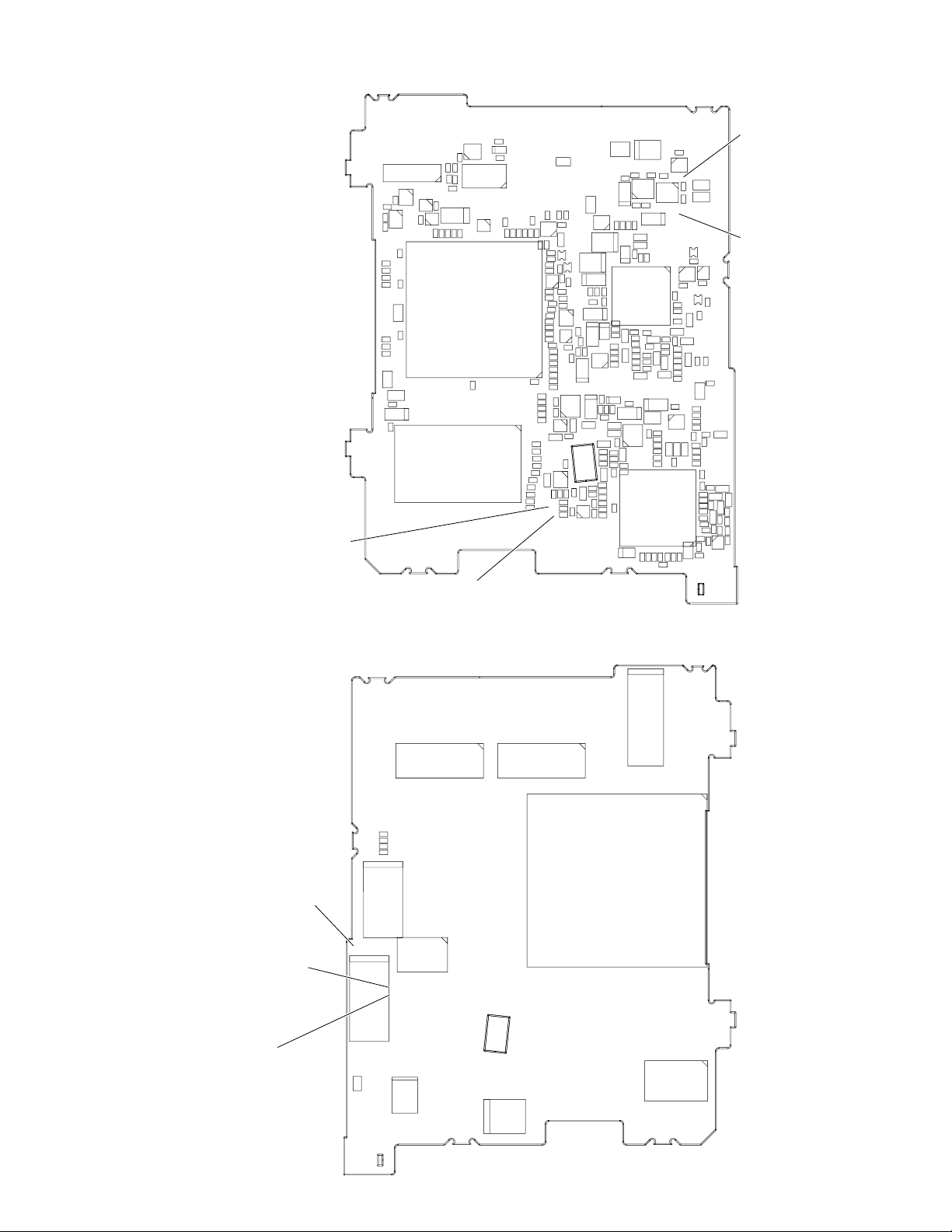
(Wiring board diagram: Sub Side A)
TL6606(INT MIC L)
EE level
Frequency character
VL-AX1U
TL2732
TL2731
TL2730
TL2728
TL3781
TL2724
TL2722
TL2720
TL2718
TL2712
TL2706
TL2704
X3750
TL3796
TL3793
TL3795
Q3709
R3719
Q3702
R3718
TL3780
Q3708
R3714
R3717 C3718
TL3712
C3715
R3780
TL3704
TL3729
R3775
TL3711
R3779
TL3709
R3762
R3715
C3701
TL3702
TL3710
TL3707
C3708
R3778
TL3708
R3777
TL3706
R3776
TL3705
L3701
FB3701
C3711
C3709
C3710
TL3727
TL3719
TL3713
TL3717
TL3721TL3718
TL3726TL3724
TL3714
TL2721
TL2726
TL2716
TL2719
TL2725
TL2715
TL2717
TL2711
TL2710
TL2714
TL2709
TL2708
TL3750
D3751
TL2751
TL2707
TL2702
R3753
TL2750
C3752
R3752
IC3750
C3753
R3751
TL3794
C3751
TL3797
TL3799
TL2713
TL3792
R3781
TL3777TL3776
FL3701
Q3703
TL3775
R3713
C3707
C3706
R3716
R3712
IC3701
TL2701TL3798
TL2705
TL2703
C3705
IC3702
TL3725TL3722
TL3720
TL6607(INT MIC R)
EE level
Frequency character
TL2723
C3750
TL3766
TL2727
D3750
TL2729
R3750
TL2739
TL2740
TL2741
TL3784
TL3786
TL3778
TL3783
TL3782
TL3785
Q3707
C3714
TL3791
TL3779
TL3789
TL3790
R3710
C3704
TL3716
TL3715
0
TL3756
TL3760
TL3769
TL3787
TL3758
TL3764
TL3757
TL3762
TL3759
TL3773
TL3771
TL3768
TL3767
TL3788
TL3772
R3769
R3765
R3771
TL3754
C3755
R3770
TL3755
Q3701
C3754
R3735
R3772
R3711
R3784
TL3801
TL2761
TL3728
TL3723
R3818
R3812
TL3765
C3702
R3773
R3733
R3721
R3732
R3734
R3731
R3720
R3800
TL3800
R3783
Q3706
R3737
R3730
C3712
TL3703
R3705
R3774
TL3770
R3729
R3728
R3727
R3726
R3725
Q3705
R3724
R3723
R3722
Q3704
R3797
R3786
R3796
R3799 R3787
R3795
R3798
R3794
R3793
R3792
R3791
C3703
TL3701
R3790
TL2760
R3808
R3809
R3810
IC6602
R3803
R6645 C6642
R3804
Q6606
C6652
R6644
C6653
R3813
R3814
R3817
R3819
R6642
R3815
R3816
Q6603
C6651
R3811
R3801
R6643
R6625
R6626
R6627
C6603
TL6605
TL6606
C6608
Q6602
TL6607
R6612
C6650
TL3752
TL3742TL3739
TL3743
L603
C635
TL3749
TL3738
TL3751
R689
R687
R663
R685
Q608
C685
TL3753
TL3744
L601
TL3761
TL3763
C640
C639
R654
R670
C633
C632
R3788
R3789
C3717
C6657
C6654
R6616
R6611
C6611
R686
R688
TL3774
Q606
C642
R638
TL3746
Q609
R6660
C6655
R6658
C6612
R6619
R6618
C6613
R6617
R6615
C6605
R6603
C6607
C6602
R6624 R6604
C686
C690
R656
R651
C651
TL3748
C646
C637
R641
C638
R640
R639
IC601
R658 C605
C645
R635
C629
C624
C631
R657
R632
C628
C623
R630
C621
R626
R628
R631
R621
R648
R649
D6601
R6657
R6659
C6616
C6615
R6621
C6619
C6618
C6614
R676
R624
R633
C641
C644
C661
C626
R634
R653
C647
C625
R6656
C6643
C6656
L6601
R6646
C6648
Q6608
R6648
R6647
R6623
R6649
R6650
C6617
R6651
R6622
C6620
R6620
IC6601
C6610
C6604
C6621
R6628
C6622
R6664
R6629
TL3747
TL3745
TL602
R610
TL3737
Q602
TL3730
TL605
Q601
R603 R609
TL3733
TL3731
TL3735
TL604
TL3732
TL3734
TL3736
R655
R662
TL3741
TL3740
Q604
R661
C611
C610
C608
C607
C606
C617
R652
C619
R667
R623
R673
R625
C618
C648
R668
C622
R627
R647
R6607
C6606
R6606
Q6609
FB6601
C6601
R6653
C6646
C6644
C6645
C6647
R6640
C6641
R6652
C6624
C6628
R6630
R6665
R6666
C6630
TL605
EE level
Frequency character
Super-directional microphone
C603
C616
TL604
EE level
Frequency character
Q605
Super-directional microphone
R660
R614
R616
R613
R6671
R6672
FB6602
C6684
R6641
C6637
R6639
C6640
C6639
C6638
R6638
R6636
C6636
C6634
C6635
R6635
R6634
C6633
R6633
C6631
C6632
R6632
C6659 R6637
C6629
R6663
C6660 R6662
C6658 R6661
C6626
Q6607
C6623
(Wiring board diagram: Sub Side B)
TL6609(GND)
EE level
Frequency character
Super-directional microphone
TL6608(TELE-MIC)
Super-directional microphone
TL6610(OPEN)
EE level
Frequency character
Super-directional microphone
SC3706
SC3705SC3704
R3802
R3805
R3806
R3807
SC3701
TL2755
TL2754
SC3707
TL2752
TL2759
TL2733
TL6609
TL2753
TL2756TL2757
TL2758
TL6601
1
SC6602
SC3703
TL6611
TL6608
TL6610
BAT3750
SC3702
SW3702
P6601
27
Page 28
VL-AX1U
[Making adjustments]
Adjusting the servo system controller and related parts
1. Setting the system codes
Replacement of IC705 E2PROM requires the following data to be set in this order.
[Procedure]
Set the unit to the VCR mode and set the data for each address.
Code
Address 01 09 02 0A 03 0B 04 0C 05 0D 07 0F
Data 00 FF 01 FE 1C E3 00 FF 00 FF 02 FD
When replacing the IC705 E2PROM, first make the following settings and then start the adjustments.
(1) Electromagnetic conversion
Address 27 28 2B *105 25 26
Data 40 90 90 80 40 90
* The address uses only when replacing the IC302.
• Manual adjustment
Mode VCR ADJ mode
Procedure 1) Set the CAM/OFF/VCR selection switch to VCR.
Examples • During E
1. Model code 2. Destination code 3. Specifications code 4. Menu selection code 5. Software switching code 6. Calendar switching
2) Press “CONTINUE” → ”VCR adjustment” on the remote controller to set the VCR adjustment mode.
(At this time an indication “VCR ADJ” appears at the left lower side.)
Enter a setting corresponding to the address.
<Setting method>
3) Adjust the address by moving up and down the blinking numeral with the FF and REW key, and fix the address
by pressing the PB key.
4) Adjust to the setting by moving up and down the blinking numeral with the FF or REW key, and set data by
pressing the PB key.
5) Press the STOP key to set the address set state.
6) Repeat the operations 3), 4) and 5) as much as input addresses. After completion of input of all items hold
down the “CONTINUE” key to cancel the VCR adjustment mode.
7) Set the CAM/OFF/VCR selection switch to OFF.
2
PROM (IC705) replacement.
2. HSWP adjustment
Mode VCR ADJ mode
Procedure 1) Play back the alignment tape in the video mode.
2) Press the "CONTINUE" and "HSWP ADJ" keys on the adjustment remote control in this order.
→ This executes the HSWP adjustment.
When the adjustment is successful, the LCD lights up [OK] and the cassette is automatically ejected. If not
properly adjusted, the LCD lights up [NG].
Examples • During mechanism replacement. • During E2PROM replacement (IC302 inside the head amplifier circuit board).
3. SHUT OFF adjustment
Mode VCR ADJ mode
Procedure 1) Load a recordable tape, and set the camera mode.
Press the "CONTINUE" and then the "TEST SEL" on the remote control for adjustment to enter the TEST mode (T-01 blinks).
2)
3) Select T-03 with the FF or REW key and then press the PB key. (By the remote control)
4) Observing the power voltage from TL900(-), set it so that TL904(+) obtains 6.00V ± 50mV.
5) Press the playback key on the main unit. Turn off the power and the adjustment is completed.
Examples • During microcomputer (IC704) or E
2
PROM (IC705) replacement.
28
Page 29
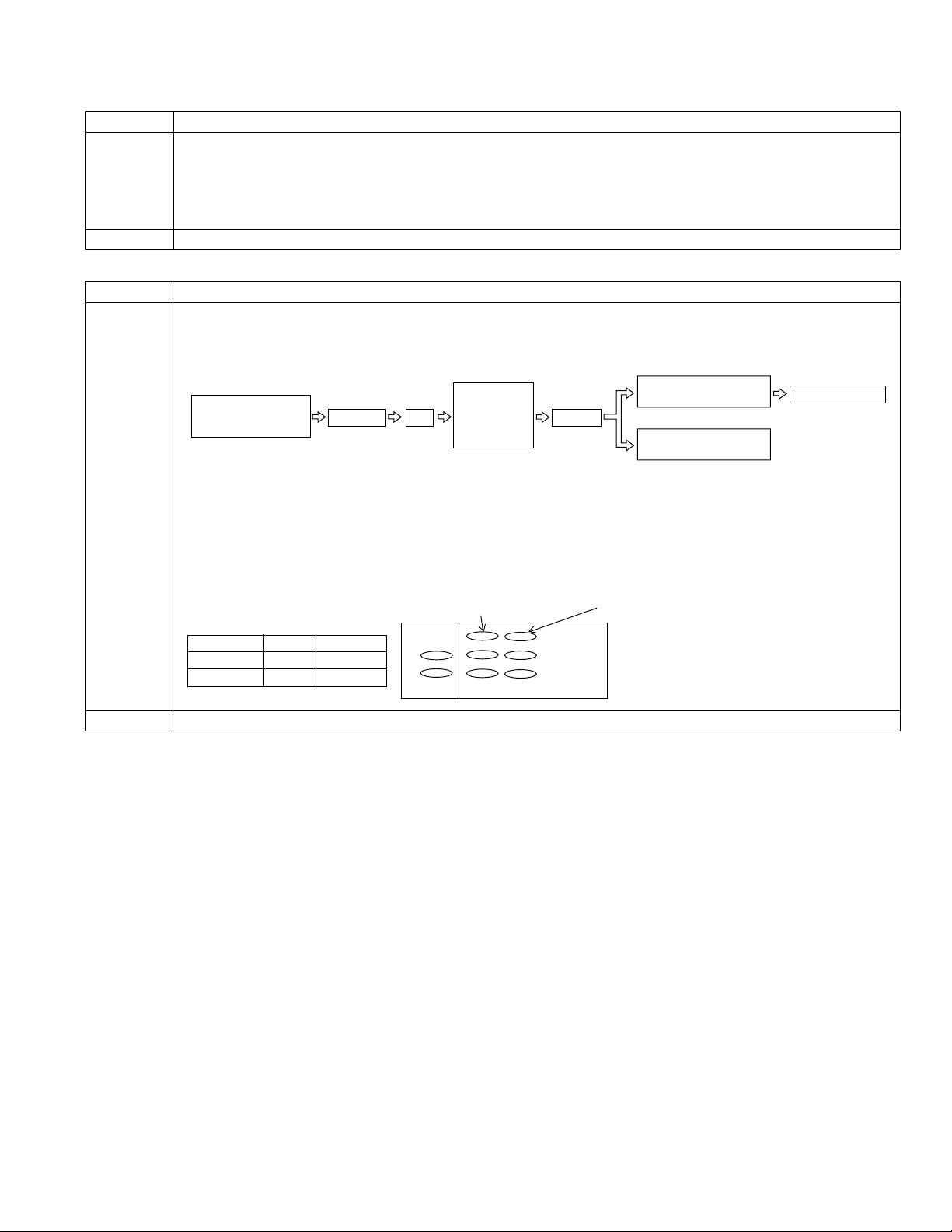
ADJUSTING THE ELECTROMAGNETIC CONVERSION CIRCUIT SYSTEM
1. PLL VCO adjustment
Mode VCR ADJ mode
Procedure 1) Playback the alignment tape (or a self-recorded tape).
2) Call the adjustment mode (V-ADJ).
3) Set the address "2A" and call the data.
4) Set the called data with the FF/REW key to the point where the playback screen appears.
(At this time, the screen full of block noise is OK.)
Examples • During E
2. Phase and equalizer adjustment → (Performed in the VCR mode)
Mode VCR ADJ mode
Procedure 1) Load a self-recorded tape into the deck.
2) After playback for 3 minutes, select the test mode 0F using the remote control for adjustment to start the
automatic adjustment. (The following sequence is automatically performed.)
2
PROM replacement. • During circuit board (Main) replacement.
VL-AX1U
The built-in VI/O
colour bar is recorded.
VS REW
PB
Phase and
equalizer are
adjusted
automatically.
OK:
Blue LCD comes on.
Judgment
NG:
Red LCD comes on.
Tape is EJECT.
3) A power source is put again after a power source is cut once.
4) Error rate check
Select and fix the TEST MODE 0B on the adjustment remote control.
5) Manual adjustment method (video adjustment mode)
* Perform this adjustment with the self-recording/playback in the LP mode.
For phase, vary the data for the address 26 and 2B, and for equalizer, vary the data for the address 25 and 27,
to set the error rate is made as small as possible.
Error rate
Synchronization error 20 or less
Error rate 200 or less (SP Mode)
330 or less (LP Mode)
Phase Equalizer
H ch side 2B 27
L ch side 26 25
Synchronization error
H
L
Examples • During mechanism replacement. • During circuit board (Main) replacement. • During E2PROM replacement.
29
Page 30
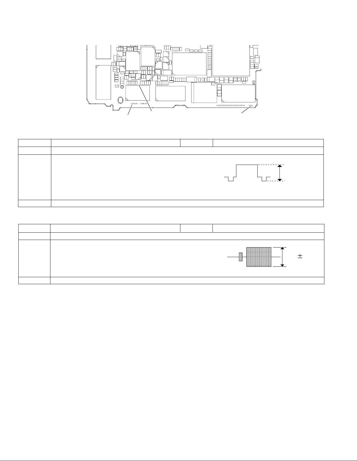
VL-AX1U
;
;
;
;
y
y
y
y
TL783
7
TL5756
5
R2589
5
5
C
R
R
B
ADJUSTING THE VIDEO I/O CIRCUIT SYSTEM
(Wiring board diagram: Main Side B)
TL5760
TL5758
TL8840TL8842TL8841TL8843
TL911
TL2811
TL2813
TL2814
TL2818
TL2819
TL2825
TL1913
TL1909
TL2834
SC5
TL2812
TL2817
TL2816
TL2820
SC2801
TL2833
TL5761
R2583 R25R2588 R2
R2582
TL5759
Q2510
R2832
C2805
R2812
C2807
D2801
R2833
R2815
TL2804
R2814
Q2800
R2811
R2813
R2810
C2808
TL2803
R2825
R2831
R2823
R2818
R2822
R2820
TL2815
R2819
R2824
TL1908
TL1475
PCO D/A-Y
R2592
C2548
R2594
R2581
R2605
C2551
R2615
C2552
R1470
R2
R25C2
R2590
C2544
C2546
C2542
R2593
IC2507
R2610
R2617
R2606
R2604
R2616
D2504
R2623
TL1480
TL1477
R1471
R1476
R1472
FB1472
SC1401
TL1475TL1478 TL1481TL1479
IC2502
R2529
R2528
R2526
R2530 R2521
C2520 R2520
C2517 C2518
D2501 R2519 R2522
R1477
R1473
R1475
R1474
FB1471
TL1477
PCO D/A-C
TL5789
R2527 R2525
Q2501
TL5790
C2513
R2534
Q2508
R2517
TL5788
TL5786
R2513
R2510
Q2507
R2537
R2523
R521
R522
Q2502
Q2504
R2533
Q2503
C2511
L2502
TL2800
C2553
C2554
R2518
R2524
SC2501
TL5752
TL5778
TL4403
TL4405
R523
TL7801
C2555
C2556
R2538
C2530
C2531
R2532
IC2501
C2504
C2502
C2508
R2502
R2501
C2506
C2505
C2503
TL2802
TL2801
L501
TL4404
R2503
R2505
C2507
R2504
C2501 C2510
TL912
R796
R2506
SC701
C224
R205
C222
C5702
C5704
C5703
C5701
C239
C210
C208
R235
L2501
C2509
R797
C204
IC201
R203
R207
R208
R202
TL238
R213
R201
TL239TL245TL244TL243TL242TL241TL235TL240
TL1431
R204
TL237
SC201
TL1420
PCO D/A-Y
PCO D/A-C
1. PCO D/A-Y adjustment
Test point TL1475 (connected to oscilloscope) Address VCR ADJ 22
Mode EE mode
Procedure 1) Connect TL1420 to GND.
2) Connect the AVS cable and then connect it to the monitor (TO).
3) Call the adjustment mode (V-ADJ).
4) Set the address to "22", and call the date.
(100% white signal is output.)
5) Vary the date with the FF and REW keys to set the signal appearing at TL1475 to 1.0Vp-p ± 0.05Vp-p.
Examples • During E
2
PROM replacement. • During IC4401 replacement. • During IC1401 replacement.
F
TL908
TL4441
L204
C215
C213
C212
C211
C209
R251
R257
R255
TL234
TL4437
TL4438
TL4439
TL233
TL202
R243
R242
C205
R206
TL201
R258
TL236
R244
TL1420
1.0±0.05
2. PCO D/A-C adjustment
Test point TL1477 Address VCR ADJ 23
Mode EE mode
Procedure 1) Connect TL1420 to GND.
2) Connect the AVS cable and then connect it to the monitor (TO).
3) Call the adjustment mode (V-ADJ).
4) Set the address to "23", and call the data.
5) Vary the data with the FF and REW keys to set the signal appearing at TL1477 to 0.62Vp-p ± 0.05Vp-p.
Examples • During E2PROM replacement. • During IC4401 replacement. • During IC1401 replacement.
;;;;
yyyy
;;;;
yyyy
;;;;
yyyy
;;;;
yyyy
0.62 0.05
30
Page 31

ADJUSTING THE LCD CIRCUIT
F
* To make this adjustment, set the backlight switch to the "NORMAL" position.
(Wiring board diagram: Main Side B)
TL4440
TL7800
R509
C507
R526
TL4403
TL4404
TL4405
R2503
TL7801
C2530
C2531
C2501 C2510
R2505
IC2501
C2507
R2504
C2508
R2502
R2501
TL2801(G OUT)
DAC full-scale
C202
C501
L501
R796
R2506
SC701
FB203
C224
R205
TL912
C222
C5702
C5704
C5703
C5701
C239
C210
C208
R235
L2501
C2509
R797
TL7823
C231
C223
R209
R202
C204
R213
R201
TL1431
TL239TL245TL244TL243TL242TL241TL235TL240
C226
C227 C228 C240 C235
IC201
R204
R203
R207
R208
TL237
TL238
SC201
TL2802(B OUT)
DAC full-scale
R242
C205
R206
R258
TL236
Adjustment procedure and connecting same as the VCR section.
TL8855
TL8861
TL5760
TL5758
TL783
TL911
TL2811
TL2813
TL2814
TL2818
TL2819
TL2825
TL1913
TL1909
TL2834
R407
R412
C405
R416
TL8840TL8842TL8841TL8843
C404
TL3322
TL3320
SC5704
SC2801
TL2833
TL2812
TL2817
TL2816
TL2820
TL403
C508
TL416
TL417
IC503
TL4436
TL5768
TL5756
R2589
R2592
C2548
TL5761
R2582
R2583 R2584
R2588 R2585
R2594
TL5759
R2814
R2811
C2542
Q2510
R2581
R2832
C2805
R2812
C2807
D2801
R2833
R2815
TL2804
Q2800
R2813
R2617
R2605
R2810
C2808
C2551
TL2803
R2825
R2616
R2831
R2823
R2615
C2552
R2818
R2822
R2820
TL2815
R2819
R1470
FB1472
R2824
TL1908
TL5776
R2516
R2512
R2586
R2587
R2590
C2546
R2593
IC2507
R2610
R2606
R2604
R2623
R1471
R1476
TL1480
TL1477
R514 C504
C513
R519
R520
C515
R516
C516
R518
Q504
C514
R517
R537
R2509
R2514
R2511
C2516
C2515
C2512 R2507
R2515 R2508
C2549
C2544
IC2502
R2529
R2528
R2526
C2520 R2520
C2517 C2518
D2504
D2501 R2519 R2522
R1472
R1474
R1477
R1473
R1475
FB1471
SC1401
TL1475TL1478 TL1481TL1479
IC501
TL5789
TL5790
TL5788
R521
R522
R523
TL5786
C2555
C2556
C2513
R2513
R2534
Q2507
Q2508
R2530 R2521
R2527 R2525
R2537
Q2501
R2523
R2517
R2538
TL5752
Q2502
R2510
TL5778
Q2504
R2533
R2532
Q2503
C2511
L2502
C2504
C2502
C2506
C2505
C2503
TL2802
TL2801
TL2800
C2553
C2554
R2518
R2524
SC2501
TL2804(VGL)
COMMON PULSE
TL2803
COMMON PULSE
TL2800(R OUT)
DAC full-scale
1. VCO free-run adjustment
Test point TL7800(AFC) Address VCR ADJ 32
Mode VCR AV input
Procedure 1) Input the white 100% signal to AV input.
2) Connect the digital voltmeter to TL7800, and adjust DC voltage value to the specified adjustment value with
VCR ADJ 32.
Adjustment 2.00 ± 0.1V
rating
Examples • During E
• During DAC (IC4701) replacement.
2
PROM (IC705) replacement. • During VIO ENG (IC4401) replacement.
VL-AX1U
C203
FB204
TL908
TL4441
L204
C215
C213
C212
C211
C209
R251
R257
R255
TL234
TL7800(AFC)
TL4437
TL4438
TL4439
VCO free-run
TL233
TL202
R243
TL201
R244
TL1420
2. DAC full-scale adjustment
Test point TL2800(R OUT), TL2801(G OUT), TL2802(B OUT)
Address VCR ADJ 3D(R), VCR ADJ 3E(G), VCR ADJ 3F(B)
Mode VCR AV input
Procedure 1) Set the VCR ADJ 83/93/C0 to 00/77/00. (At this time, LCD can not be displayed.)
2) With the VCR ADJ 3D, adjust the output voltage of TL2800 and the DC voltage value of the digital voltmeter to
the specified adjustment values.
3) Similarly with the VCR ADJ 3E/3F, adjust the output voltage of TL2801/2802 and the DC voltage value of the
digital voltmeter to the specified adjustment values. (Same as Item (2))
4) Return the VCR ADJ 83/93/C0 to the initial value. (Initial value: C5/7F/28)
Adjustment 0.78V ± 10mV
rating
Examples • During E2PROM (IC705) replacement. • During VIO ENG (IC4401) replacement.
• During DAC (IC4701) replacement.
3. COMMON PULSE adjustment
Test point TL2804(VGL) Address VCR ADJ 29(C)
Mode VCR AV input
Procedure 1) Connect TL2803 to GND.
2) Set the VCR ADJ 93 to A0.
3) With VCR ADJ 29, adjust the output voltage of TL2804 and the DC voltage value of the digital voltmeter to the
specified adjustment values.
4) Return the VCR ADJ 93 to the initial value. (Initial value: 7F)
Adjustment 6.95V ± 50mV
rating
Examples • During E2PROM (IC705) replacement. • During DAC (IC4701) replacement.
31
Page 32

VL-AX1U
Q2501
3
80
R
C237
1
9
4. COM-Bias adjustment
Test point LCD panel display area Address VCR ADJ 33
Mode VCR AV input
Procedure 1) Input white 40% signal into the AV input.
2) Set the illuminometer (TOPCON IM-3) on the LCD panel surface. (Shut off the external light.)
3) Minimize the ripple of output waveform of illuminometer.
Adjustment Minimum
rating
Response time : 0.6 sec.
Remark Make this adjustment after 5-minute or longer aging.
Examples • During LCD panel replacement. • During IC705, IC4401, IC4701 replacement.
5. White Balance adjustment
Test point LCD panel daisplay area Address VCR ADJ 84(R), VCR ADJ 86(B)
Mode VCR AV input
Procedure 1) Input white 40% signal into the AV input.
2) Input white 40% signal into the standard monitor, and adjust it until it becomes the same as that screen.
Adjustment Standard monitor
rating
Remark Make this adjustment after 5-minute or longer aging.
Examples • During LCD panel replacement. • During IC705, IC4401, IC4701 replacement.
VIDEO I/O ENG DAC CIRCUIT
(Wiring board diagram: Main Side B)
FB203
C224
R205
TL912
C222
C5702
C5704
C5703
C5701
C239
C210
C208
R235
C2509
R797
C231
C223
R209
L2501
R202
C204
R213
R201
TL1431
TL239TL245TL244TL243TL242TL241TL235TL240
C
R1934 R1935
TL7823
R208
IC202
C226
C227 C228 C240 C235
IC201
R203
R207
R204
TL237
TL238
SC201
C238
Q1
TL4405(B-Y OUT)
DAC_B-Y
TL7823(GND)
DAC_Y,
C203
DAC_R-Y,
FB204
DAC_B-Y
TL908
TL4441
L204
C215
TL4404(R-Y OUT)
C213
C212
DAC_R-Y
C211
C209
R251
R257
R255
TL234
TL4437
TL4438
TL4439
TL233
TL4403(Y OUT)
TL202
R243
R242
C205
R206
TL201
TL1420
DAC_Y
R244
R258
TL236
C5
R53C50C5
5789
TL5790
C2513
R2534
Q2508
R2517
TL5788
TL5786
R2513
R2510
Q2507
R2537
R2523
R53C50R50R50C50R53R5
R521
Q2502
Q2504
R2533
Q2503
C2511
L2502
TL2800
C2553
C2554
R2518
R2524
SC2501
IC501
R522
TL5752
TL5778
R506
TL5780
C230
FB201
TL4440
TL7800
R509
C507
R526
C202
C501
TL4403
TL4405
R523
TL7801
C2555
C2556
R2538
C2530
C2531
R2532
IC2501
C2504
C2502
C2508
R2502
R2501
C2506
C2505
C2503
TL2802
TL2801
L501
TL4404
R2503
C2501 C2510
R2505
C2507
R796
R2506
R2504
SC701
6. DAC_Y adjustment, DAC_R-Y adjustment, DAC_B-Y adjustment
Test point TL4403(Y OUT), TL4404(R-Y OUT), TL4405(B-Y OUT), TL7823(GND)
Mode CAM
Address VCR ADJ FA(Y), VCR ADJ FB(R-Y), VCR ADJ FC(B-Y)
Procedure 1) Set VCR ADJ 303/304/432/423/424/425/426 to 0C/EF/63/90/EB/80/80.
Adjustment 0.450V ± 5mV (Y OUT), 0.229V ± 2mV (R-Y OUT), 0.290V ± 2mV (B-Y OUT)
rating
Examples • During IC705, IC4401, IC4701 replacement.
2) With VCR ADJ FA, adjust the output voltage of TL4403 and the DC voltage value of the digital voltmeter to the
specified adjustment values.
3) Similarly with VCR ADJ FB/FC, adjust the output voltage of TL4404/TL4405 and the DC voltage value of the
digital voltmeter to the specified adjustment values. (Same as Item (2))
4) Return VCR ADJ 303/304/432/423/424/425/426 to the initial value. (Initial value: FF/FF/43/10/29/6E/F0)
Note:When it is changed to the initial value FF/FF/43/10/29/6E/F0, OSD display goes out together with LCD/VF.
Checking the monitor output, adjust it. After adjustment, be sure to return to FF.
32
Page 33

(Wiring board diagram: Main Side B)
4
S
C701
R1943
VL-AX1U
TL4440
TL7800
R509
C507
R526
C2501 C2510
D1900
C230
FB201
C202
C501
L501
R2506
SC701
Q1920
R1911
TL912
C5702
C5704
C5703
C5701
R797
R796
R1912
C237
C231
FB203
C223
R209
C224
R205
C222
C239
C210
C208
R235
L2501
C2509
C204
TL1431
C1994
R1934QR1935
IC202
TL7823
C226
IC201
R207
R208
R202
R213
R201
TL239TL245TL244TL243TL242TL241TL235TL240
TL8843(VB)
VF sub-brightness R/B
TL8861(BLD)
VF VCO
TL8841(VG)
VF COM-DC
VF brightness
VF contrast
VFγ1
VF sub-brightness R/B
TL8840
VF COM-DC
TL8842(VR)
VF sub-brightness R/B
R406
R416
TL8855
TL8861
TL783
TL5760
TL5758
TL8840TL8842TL8841TL8843
TL911
TL2811
TL2813
TL2814
TL2818
TL2819
TL2825
TL1913
TL1909
TL2834
IC
R442
C452
R443
R446
C451
C407
R411
Q1947
R1992
C404
R407
R412
C405
TL3322
TL3320
SC5704
SC2801
TL2833
TL2812
TL2817
TL2816
TL2820
R1721
R1720
TL3321
TL403
C508
TL416
TL417
TL4436
TL5768
TL5756
TL5761
TL5759
C2805
R2833
R2815
TL2804
R2814
R2811
C2808
R2825
R2823
R2822
TL2815
R2824
TL5776
IC503
R2516
R2512
R2589
R2587
R2586
R2592
R2590
C2548
C2546
R2582
R2583 R2584
R2588 R2585
R2594
C2542
R2593
Q2510
R2581
R2832
R2812
C2807
D2801
IC2507
Q2800
R2813
R2610
R2617
R2605
R2810
C2551
TL2803
R2606
R2604
R2616
R2831
R2623
R2615
C2552
R2818
R2820
R2819
R1471
R1476
R1470
FB1472
TL1908
SC1401
TL1475TL1478 TL1481TL1479
C2549
TL1480
TL1477
R1472
TL5770
C512
R535
C4702
TL5767
FL501
R514 C504 R531
C513
R519
R520
C515
R516
C516
R518
Q504
R517
C514
R537
R2509
R2514
R2511
C2516
C2515
C2512 R2507
R2515 R2508
TL5789
TL5790
C2544
R2526
D2504
C2517 C2518
R1475
TL5788
TL5786
C2513
R2510
R2513
IC2502
R2534
R2533
Q2507
R2528
R2529
Q2508
R2530 R2521
R2527 R2525
C2520 R2520
R2537
D2501 R2519 R2522
Q2501
R1473
R1477
R1474
R2524
R2523
R2517
FB1471
C502
C511
R536
C503
IC501
R521
R522
TL5752
Q2502
TL5778
Q2504
Q2503
C2511
L2502
TL2800
C2553
C2554
R2518
SC2501
TL5781
R505
R504
R523
C2555
C2556
R2532
C2504
C2502
C2503
TL2802
TL2801
R780
C509
R532
R533
R506
TL5780
TL4404
TL4403
TL4405
R2503
TL7801
R2538
C2530
C2531
R2505
IC2501
C2507
R2504
C2508
R2502
R2501
C2506
C2505
7. VF VCO adjustment
Test point TL8861(BLD) Address VCR ADJ E1
Mode VCR AV input
Procedure 1) Connect TL7801 to GND. (No signal)
2) Connect TL8861 to the frequency counter, and adjust the frequency to the specified adjustment value with the
VCR ADJ E1.
Adjustment 15.734 ± 0.1KHz
rating
Examples • During IC705 or IC8800 replacement.
Q1938
C227 C228 C240 C235
R206
R204
R203
TL236
TL237
TL238
SC201
R1940
C1921
C238
Q1913
TL7801
C203
VF VCO
FB204
TL908
TL4441
L204
C215
C213
C212
C211
C209
R251
R257
R255
TL234
TL4437
TL4438
TL4439
TL233
TL202
R243
R242
C205
TL201
R258
R244
TL1420
8. VF COM-DC adjustment
Test point TL8840 Address VCR ADJ F6
Mode VCR AV input
Procedure 1) Input the signal of a 3-step waveform.
2) Read the DC voltage value of the output of TL8841 with the digital voltmeter. (VG
3) Similarly rad the DC voltage value of the output of TL8840 with the digital voltmeter. (VCOM
4) Adjust the value of (VCOMDC - VGDC) to the specified adjustment value.
Adjustment -0.15 ± 0.1V
rating
Examples • During IC705 or IC8800 replacement.
9. VF brightness adjustment
Test point TL8841(VG) Address VCR ADJ E0
Mode VCR AV input
Procedure 1) Input the signal of a 3-step waveform.
2) Set VCR ADJ ED to 00.
3) Adjust the waveform pedestal range of TL8841 to the specified adjustment value.
4) Return VCR ADJ ED to the initial value. (Initial value: 7A)
Adjustment 7.4Vp-p ± 0.1Vp-p
rating
Sig. center
7.4Vp-p 0.1Vp-p
)
DC
)
DC
GND
Examples • During IC705 or IC8800 replacement.
33
Page 34

VL-AX1U
10. VF contrast adjustment
Test point TL8841(VG) Address VCR ADJ E5
Mode VCR AV input
Procedure 1) Input the signal of a 3-step waveform.
2) Set VCR ADJ EB/ED to FF/00.
3) Adjust the pedestal 100% range of the waveform of TL8841 to the specified adjustment value.
4) Return VCR ADJ ED to the initial value. (Initial value: 7A)
Adjustment 2.0Vp-p ± 0.1Vp-p
rating
GND
2.0Vp-p 0.1Vp-p
Examples • During IC705 or IC8800 replacement.
11. VFγ1 adjustment
Test point TL8841(VG) Address VCR ADJ EB
Mode VCR AV input
Procedure 1) Input the signal of a 3-step waveform.
2) Set VCR ADJ ED to 00.
3) Adjust the white 100% range of the waveform of TL8841 to 5.6±0.1Vp-p with VCR ADJ EB.
4) Then adjust the same waveform VCR ADJ E5 to 3.2±0.1Vp-p.
5) Return VCR ADJ ED to the initial value. (Initial value: 7A)
Adjustment 5.6 ± 0.1Vp-p (VCR ADJ EB)
rating 3.2 ± 0.1Vp-p (VCR ADJ E5)
Sig. center
5.6Vp-p 0.1Vp-p
3.2Vp-p 0.1Vp-p
GND
Examples • During IC705 or IC8800 replacement.
12. VF sub-brightness R/B adjustment
Test point TL8842(VR), TL8841(VG), TL8843(VB) Address VCR ADJ E9(R), VCR ADJ EA(B)
Mode VCR AV input
Procedure 1) Input white 40% signal into the AV input and standard monitor.
2) Adjust it with the VCR ADJ E9/EA so as to obtain the same color as the standard monitor.
Adjustment Standard monitor
rating
Examples • During IC705 or IC8800 replacement.
34
Page 35

ADJUSTING THE MIC AMP CIRCUIT
C690
R6615
3
(Wiring board diagram: Sub Side A)
VL-AX1U
52
TL3742TL3739
TL3743
TL602
C635
TL3737
TL3738
87
R689
R663
TL3730
Q608
Q601
688
R686
TL3774
C686
C646
C637
R3801
R3818
TL3725TL3722
R3812
TL3716
TL3715
TL6606(INT MIC L)
EE level
Frequency character
TL3745
R610
Q602
TL605
C603
C616
R603 R609
TL3731
TL3733
TL604
TL3735
TL3732
TL3734
TL3736
R6626
R6625
R6627
C6603
TL6605
TL6606
C6608
TL6607
R6612
TL6607(INT MIC R)
EE level
Frequency character
TL3747
TL605
EE level
Frequency character
Super-directional microphone
TL604
EE level
Frequency character
Super-directional microphone
R6611
R664
C6611
C6605
R6603
C6607
C6610
Q6602
C6602
C6650
R6624 R6604
C6604
IC6601
C6621
R6628
C6622
R6664
R6665
R6666
C6630
R6629
TL6609(GND)
EE level
Frequency character
Super-directional microphone
TL6608(TELE-MIC)
Super-directional microphone
TL6610(OPEN)
EE level
Frequency character
Super-directional microphone
(Wiring board diagram: Sub Side B)
TL6609
TL6601
1
TL2758
SC6602
SC3707
TL2753
TL2756TL2757
TL6611
TL6608
TL6610
1. EE level check
Measuring instrument Valve voltmeter Test point TL605, TL604
Mode P-ON (CAM), Zoom MIC "OFF", Adjustment rating -9dBs ± 3dB
Timbre mode "NORMAL" ,
Wind sound decrease "OFF"
Test signal 1kHz -54dBs sine wave
Procedure 1) Input 1kHz, -54dBs sine wave into TL6606(INT MIC L) and TL6607(INT MIC R).
2) Make sure that the signal level of TL605 Audio-L out and TL604 Audio-R out is within the standard
limits.
Remark TL6610: OPEN, TL6609: GND
TL2755
TL2754
TL2752
TL2759
TL2733
SC3703
SW3702
2. Frequency character check
Measuring instrument Valve voltmeter Test point TL605, TL604
Mode P-ON (CAM) Adjustment rating
(1kHz standard)
100Hz: -11dBs ± 3dB
Parameter: Zoom MIC "OFF", 10kHz: 0B ± 3dB
Timbre mode "NORMAL",
Wind sound decrease "OFF"
Test signal 100Hz, 10kHz -54dBs sine wave
Procedure 1) Input 100Hz, -54dBs sine wave and then 10kHz, -54dBs sine wave into TL6606(INT MIC L) and
TL6607(INT MIC R).
2) At this time make sure that the signal level of TL605 Audio-L out and TL604 Audio-R out is within the
standard limits (1kHz standard).
Remark TL6610: OPEN, TL6609: GND
3. Super-directional microphone check
Measuring instrument Valve voltmeter Test point TL605, TL604
Mode P-ON (CAM), Zoom MIC "TELE", Adjustment rating -10dBs ± 3dB
Timbre mode "NORMAL",
Test signal 1kHz -54dBs sine wave
Procedure 1) Input 1kHz, -54dBs sine wave into TL6608(TELE-MIC).
Remark TL6610: OPEN, TL6609: GND
Wind sound decrease "OFF"
2) Make sure that the signal level of TL605 Audio-L out and TL604 Audio-R out is within the
standard limits.
35
Page 36

VL-AX1U
DV INTERFACE (IEEE1394) ID SETTING
This unit has a DV interface function conforming to IEEE1394. Therefore, each individual ID number must be used for each unit. Since this ID is written
on the E
■ ID code is acquired
1. Connect with the EUI48/64 ID code control system.
2
PROM (IC302) on the head amp PWB, the ID must be newly written when replacing this IC or the head amp PWB.
Address 180, 17F, 17E Mode VCR
Adjustmentrating ID number obtained from the URL below
Procedure 1) Refer to the ID code application below.
2) Set the data obtained in step (1) to the corresponding addresses in the VCR adjustment mode.
* (Example) The data "08001F 0100 123456" is obtained.
(1) Enter the unit in the VCR ADJ mode.
(2) Set the ID numbers as follows.
Address 180 17F 17E
Data 12 34 56
Examples • During E
2
PROM (IC302: on the H/A unit) replacement. • During the H/A unit (RAMP-0035TAN0) replacement.
(1) Start the Internet Explorer or Netscape Navigator.
(2) Access the following address.
(URL:http://www.rcg.kami.sharp.co.jp/quics/e_index.html)
Select the "EUI48/64 ID code control system" from the "Service" item.
Note: If you want to establish a connection by directly inputting the URL, please input the following.
URL:http://www1.rcg.kami.sharp.co.jp:7000/adrs_agt/adrs_dba/ide00010.main
The login screen will appear.
(3) For the [User ID], input the [Password].
Click on [Login].
(4) Click on [EUI 64 (IEEE 1394)] from the [1. Application for acquisition of ID].
Click
36
Page 37

(5) Click on [Repair use].
Click
(6) Input the necessary information for the application.
For the indispensable input items, be sure to input them.
Select the [Group/company] and [Kind name] from the list.
Input the [Model name].
Input the [Serial number].
Input the [Site/department of repair].
VL-AX1U
(7) Click on [motion].
The confirmation screen will appear.
(8) Click on [Yes].
2. Print the application result.
(1) Print out the application result screen.
Control the application result as evidence.
To print it, select "Print (P)" from the "File (F)" in the
menu bar or click on the print button in the tool bar.
(2) Click on [Menu] to complete the application.
If you create applications in succession, repeat steps
(1)~(8).
To complete it, click on [End] in the menu screen.
MODEL ID SETTING
Address VCR ADJ FD, FE, FF Mode VCR
Adjustment rating The following table reference. VL-AX1U (102022)
Procedure 1) Set the unit to the VCR ADJ mode.
Address FD FE FF
2)
Data 10 20 22
Examples • During E2PROM (IC705) replacement.
37
Page 38

VL-AX1U
10-2. Camera Section Adjustments
10-2-1. Camera section service
(1)Camera adjustment is performed after the set has been completed.
(2)Subjects, measuring instruments and jigs needed for camera section service and adjustments
• Gray scale chart • Frequency counter • Video output cable
• Color bar chart • Illumination meter • AC adapter
• Oscilloscope • Color temperature meter • Extension cables
• Digital voltmeter • Color temperature conversion filter • Remote control unit for servicing
• Halogen lamp: 2 pcs. HOYA "LB-165"
• Vector scope • Color video monitor
10-2-2. List of camera jigs and tools
Configuration
<Note: The entries of list> 1. Name 2. Part No. 3. Code
1. Gray scale chart
(390 x 520 mm)
2. JiGCHART-1
3. CP
1. Color temperature
conversion filter
(3200 degrees K ⇒ 6800
degrees K)
2. JiGHOYA-LB165
3. BN
1. Color bar chart
(240 x 320 mm)
2. JiGCHART-4
3. DA
1. PC plate connector drawer
2. JiGTH-SS10
3. AW
1. Illumination meter
(0 to 3000 lux)
2. JiGMETER-1
3. CT
1. Remote control until for
servicing
2. RRMCG0033TASA
3. BT
1. Color temperature meter
(1600 to 40000 degrees K)
2. JiGMETER-2
3. EL
10-2-3. Adjusting the camera unit
(1)Preparations for adjustments and items to be checked
1) Set up the light box so that the entire pattern is evenly lit. Set the color temperature to 3200°K.
2) Use test patterns that are not dirty nor discoloured.
3) If the electrical circuitry gets in trouble, be sure to pinpoint the trouble spot with a measuring instrument and repair or replace
the defective part.
(2)Remote control for servicing RRMCG0033TASA
To adjust the camera section of this machine, the remote control for servicing (RRMCG0033TASA) is used. The adjustment is made
in such a manner that the remote control writes necessary data by way of the microprocessor to the specific addresses on the
2
PROM (IC502).
E
1) To adjust the camera:
Press the "CONTINUE" key first and then the "CAM ADJ" key.
This will show
CAM ADJ
on the LCD screen, thereby having the camera unit ready for the adjustments.
2) Descriptions of the displays
CAM ADJ (Indicates the camera adjustment mode.)
(Address value) (Data value)
* The address values for this machine range from 0000 to 09FF.
* The data include byte data (the last two digits are effective) and 2-byte data (the last three digits are effective).
3) Descriptions of the remote control keys
"FF" key: Increases the address and data values.
"REW" key: Decreases the address and data values.
"PLAY" key: Specifies addresses and calls the data.
This key also fixes the data values.
"STOP" key: Clears the data to enable the selection of address.
38
Page 39

4) Operation flow
FF or REW PLAY PLAY STOPFF or REW
Address is selected and specified, with the data called. Then the called data are selected and
fixed. The operation flows in this sequence.
5) When the adjustment is complete:
Press the "CONTINUE" key to let the "CAM ADJ" display disappear from the screen.
Note: Before terminating the adjustments, make sure that the adjustment mode is neither the auto-focus function adjustment
mode nor the camera signal system adjustment mode (these modes are mentioned later).
• Camera unit adjustment modes
The camera unit is adjusted in two types of modes: the auto-focus function adjustment mode and the camera signal system
adjustment mode.
VL-AX1U
Note: E
2
PROM contains the adjustment item data as shown below. If it is changed, data rewriting and confirmation of latest data
must be performed.
1) E2PROM on Camera Head Section
Lens Data
2) E2PROM(IC502) on main unit
Signal system adjustment data
(3)Auto-focus function adjustment mode
• The camera unit uses a microprocessor-controlled auto-focus zoom lens.
The auto-focus circuit incorporated in this unit is designed to execute the image processing where the focusing action is done by
taking advantage of the fact that the high-frequency components in the image signals increase as the focus intensifies. Moreover,
to achieve high magnifying power with a small lens, the camera unit incorporates the inner focus system in which the focus is shifted
by moving the master lens (rear lens) back and forth. This inner focus system is a full-range focus type by which the focus can be
shifted from approximately 10 mm to the infinity. It should be noted, however, that since the closest subject distance at the telephoto
end is fixed at 1.5 m, subjects in a closer range than 1.5 m at the telephoto end will be out of focus. For this reason, the unit is
designed so the zoom control is automatically shifted to the wide angle side until the position is found where the subject can be
focused on.
In the auto-focusing system of this until, the following constitute the important factors:
• Master lens position detection data
• Iris position detection data
• Zoom lens position detection data
2
These detection data are handled and stored by the microprocessor, lens by lens, into the E
PROM.
Therefore, in the following cases, the auto-focus function adjustment is required:
• When the lens has been replaced
• When the CCD has been replaced
2
• When the E
PROM has been replaced
1) Shifting to the auto-focus function adjustment mode
Set the data for the address "0000" to " 01".
]
This makes the screen fade temporarily in white and shifts to the auto-focus function adjustment mode.
* When this adjustment mode has been shifted to, make the adjustment according to (5) Camera unit adjustment procedure.
* In this adjustment mode, the lens can not be operated.
2) Shifting to the normal operation mode
Set the data for the address "0000" to " FF".
]
This makes the screen fade temporarily in white and shifts to the normal operation mode.
]
Press the "CONTINUE" key, and the "CAM ADJ" display goes out of the screen, enabling the normal operation.
39
Page 40

VL-AX1U
(4)Camera signal system adjustment mode
In the camera signal system adjustment mode, the automatic white balance is disabled to allow for the adjustment of the camera
unit. At this time, the white balance mode is fixed at the INDOORS mode and the focus mode is switched to the manual focus mode.
1) Shifting to the camera signal system adjustment mode
Set the data for the address "0000" to " 00".
]
This shifts the camera signal system adjustment mode.
* When this adjustment mode has been shifted to, make the adjustment according to (5) Camera unit adjustment procedure.
2) Shifting to the normal operation mode
Set the data for the address "0000" to " FF".
]
This shifts the mode to the normal operation mode.
]
Press the "CONTINUE" key, and the "CAM ADJ" display goes out of the screen, enabling the normal operation.
(5)Camera unit adjustment procedure
1. Auto focus adjustment
2. Iris, ND Meter basic adjustment
3. Black balance adjustment/A/F noise adjustment
7. White balance adjustment
8. Indoor white gain adjustment
9. Color gain adjustment
4. Iris AE coarse adjustment
10. Auto white balance adjustment
5. White balance coarse adjustment
11. Outdoor white gain adjustment
6. Color gain coarse adjustment
12. Iris AE adjustment
* The above 1. Auto-focus function adjustment in the auto-focus function adjustment mode, whereas the other adjustments are made
in the camera signal system adjustment mode.
(6) Replacement procedure of gyro unit
2
1) When replacing E
Since the adjustment data of gyro is written in E
PROM on lens unit of camera head with the gyro unit not replaced
2
PROM, copy the data of addresses "0864, 0865, 0866, 0867" and rewrite them
after replacement.
2) When replacing the gyro sensor: RMC1001, RMC1002
After replacing with the specified gyro sensor, write the following data in the addresses "0864, 0865, 0866, 0867".
Ref No. Part code Address Data
RMC1002 Replacement with RSNSG0004CEZZ
RMC1001 Replacement with RSNSG0013CEZZ
0864 02
0865 30
0866 04
0867 00
40
Page 41

10-2-4. Adjustment procedures
VL-AX1U
Item
(1) Auto-focus adjustment
Set the unit to the auto-focus function adjustment mode and write data to the address "0001" one after another. This executed
the adjustments automatically. The items to be adjusted are as listed below. Every time an adjustment is made properly, the data
"00FF" is written to the address. After each adjustment, make sure that the adjustment has been made properly, and then go on
to the next adjustment item.
Address Data Adjustment item
0001 0012 WIDE end adjustment
0006 WIDE end focus ∞ position adjustment
0008 TELE end focus ∞ position adjustment
000D Zoom tracking adjustment
Note 1: To adjustment of ∞ position is executed by actually picking up the image of subject. For this adjustment use the subject with
clear profile.
Especially, if the adjustment of TELE end focus ∞ position is made without picking up the image of remote subject,
adjustment failure may occur.
Adjustment of WIDE end focus ∞ position: 3 m or more
Adjustment of TELE end focus ∞ position: 50 m or more
Note 2: In case of ∞ position adjustment the field depth is important to ensure the adjustment accuracy. If the field depth is high,
the focus becomes too stable , which may cause incorrect adjustment of ∞ position. Therefore the adjustment must be made
with low field depth (with iris opened).
The iris can be opened with the high-speed shutter.
1. It returns to the normal operation mode.
2. In the normal operation mode, set the high-speed shutter mode until the iris is opened. (Refer to the operation manual.)
3. Display “CAM ADJ” with the remote control for service.
4. It shifts to the auto-focus adjustment mode.
5. Perform the ∞ position adjustment.
6. After completing the ∞ position adjustment, return the high-speed shutter mode to the normal mode.
Adjustment method
In the camera signal system adjustment mode (write the data " 00" to the address "0000"), set the unit to the
adjustment mode.
(2)Iris/ND Meter basic adjustment
This is for adjusting the operating point of the hole element installed in the iris meter of the lens.
The adjustment is automatically done by sequentially writing the data at the address "0001" in the camera signal system
adjustment mode.The items to be adjusted are as listed below. Every time an adjustment is made properly, the data "00FF" is
written to the address.
Address Data Adjustment item
0001 0009 Hall offset adjustment
000A Iris offset adjustment
000B Iris close adjustment
(3) Black balance adjustment/A/F noise adjustment
1) Prior to the adjustment, initialize the data for the addresses "0500", "0502", "0504", "0506", "0508", "050A".
Write " FF" to all of these address.
2) Write the data " 01" to the address "0001" This starts the adjustment automatically.
When the adjustment is completed properly, the data "00FF" is written automatically.
FF
41
Page 42

VL-AX1U
Item
(4)Iris AE coarse adjustment
• Measurement terminal:
S terminal luminance signal output
(75 Ω termination)
• Address: "0002" AE_CVT
• Measuring instrument:
Oscilloscope (horizontal sync)
• Object:
Grey scale
• Data variation width:
"0000" to "00FE"
(5)White balance coarse adjustment
• Measurement terminal:
EE output
• Address:
"0128" CGAIN_KR_W
"012A" CGAIN_KB_W
• Measuring instrument:
Vector scope
• Object:
Grey scale
• Data variation width:
"0000" to "03FF"
Adjustment method
(1)Video output is observed with the oscilloscope in the grey scale standard record state,
the data of address "0002" is rewritten, and the luminance signal level is adjusted white
to 760 ± 10mVp-p, gray of the background 420 ± 10mVp-p.
100mV/div
(1)Indication on the vector scope is observed in the grey scale standard record state,
data of address "0128" and "012A" are rewritten, and an adjustment is made so that
the luminous dot is located in the position of burst ratio:
R-Y 0 ± 5%
B-Y 0 ± 5%
(6)Color gain coarse adjustment
• Measurement terminal:
EE output
• Address:
"013A" CGIN RYG
"013C" CGIN BYG
"0138" CMAT RYG
"0136" CMAT BYG
"07DE" Yellow
"07DD" Yellow phase
• Measuring instrument:
Vector scope
• Object:
Color bar chart
• Data variation width:
"0000" to "00FF"
amplitude
(1)The color bar chart is imaged, and the picture angle is adjusted so as to get white level
700 mV. Indication on the vector scope is observed, the data of address "013A",
"013C", "0138", "0136", "07DE"and "07DD" are rewritten, and setting is made so that
the red, blue and yellow luminous dots are located in the following positions. (The gain
of vector scope must be set on 75% amplitude point on the B-Y axis.)
Adjustment address
Red amplitude 1.85 ± 0.1 time (burst ratio) : "013A"
Blue amplitude 1.50 ± 0.1 time (burst ratio) : "013C"
Yellow amplitude 1.35 ± 0.1 time (burst ratio) : "07DE"
Red phase 103° ± 2° : "0138"
Blue phase 358° ± 2° : "0136"
Yellow phase 164° ± 2° : "07DD"
42
Page 43

VL-AX1U
Item
(7)White balance adjustment
• Measurement terminal:
EE output
• Address:
"0128" INDOOR_W/B R
"012A" INDOOR_W/B R
• Measuring instrument:
Vector scope
• Object:
Grey scale
• Data variation width:
"0000" to "03FF"
(8) Indoor white gain adjustment
• Measurement terminal:–
• Address: 0001
• Measuring instrument:–
• Object: White pattern
• Data variation width:–
(9)Color gain adjustment
• Measurement terminal:
EE output
• Address:
"013A" CGIN RYG
"013C" CGIN BYG
"0138" CMAT RYG
"0136" CMAT BYG
"07DE" Yellow
"07DD" Yellow phase
• Measuring instrument:
Vector scope
• Object:
Waveform monitor color bar chart
• Data variation width:
"0000" to "00FF"
amplitude
Adjustment method
(1) White balance adjustment is performed repeatedly.
(1)The adjustment is automatically done by writing the data "05" at the address "001" in
the signal system adjustment mode.
When the adjustment is normally completed, the data "FF" will be return to the address
"001". If another data except "FF" is returned, it will be judged as the poor adjustment.
(1) Color gain adjustment is performed repeatedly.
Adjustment address
Red amplitude 1.85 ± 0.05 time (burst ratio) : "013A"
Blue amplitude 1.50 ± 0.05 time (burst ratio) : "013C"
Yellow amplitude 1.35 ± 0.05 time (burst ratio) : "07DE"
Red phase 103° ± 1° : "0138"
Blue phase 358° ± 2° : "0136"
Yellow phase 164° ± 2° : "07DD"
(10) Auto white balance adjustment
• Measurement terminal:
EE output
• Address:
"000C" OUTDOOR R
"000E" OURDOOR B
• Measuring instrument:
Vector scope
• Object:
Grey scale
• Data variation width:
"0000" to "03FF"
(11) Outdoor white gain adjustment
• Measurement terminal:–
• Address: 0001
• Measuring instrument:–
• Object: White pattern
• Data variation width:–
(1)The color temperature conversion filter (LB165) is mounted in front of lens.
(2)Indication of vector scope is observed in the grey scale standard record state, and
an adjustment is made so that the luminous dots are located in the following
positions:
R-Y 0 ± 5% (burst ratio)
B-Y 0 ± 5% (burst ratio)
(1) Attach the color temperature conversion filter (LB165) in front of the lens.
(2) The adjustment is automatically done by writing the data "06" at the address "001"
in the signal system adjustment mode.
When the adjustment is normally completed, the data "FF" will be return to the
address "001". If another data except "FF" is returned, it will be judged as the poor
adjustment.
43
Page 44

VL-AX1U
Item
(12) Iris AE adjustment
• Measurement terminal:
S terminal luminance signal output
(75 Ω termination)
• Address: "0002" AE_CVT
• Measuring instrument:
Oscilloscope (horizontal sync)
• Object:
Grey scale
• Data variation width:
"0000" to "00FE"
Adjustment method
(1) Set the unit to the normal operation mode (write the data " FF" to the address
"0000").
(2)Video output is observed with the oscilloscope in the grey scale standard record
state, the data of address "0002" is rewritten, and the luminance signal level is
adjusted white to 760 ± 10mVp-p, gray of the background 420 ± 10mVp-p.
100mV/div
44
Page 45

11. USEFUL TIPS (PROBLEMS DIFFER FROM THOSE FOUND ON VHS OR
The outline looks
like a Moire pattern.
Noise bar (Green)
+ random block
noise when tape
recorded on this
unit or another
unit is played back.
8MM DECKS BECAUSE THE SIGNALS ARE DIGITALLY PROCESSED.)
VL-AX1U
Camera (EE mode)
Picture fails
to appear
Major circuits to be checked
• CCD
• Camera circuits (CDS, ADC,
CAM ENGINE)
• MEC/SYS MiCON (IC704)
• VIDEO I/O (IC1401)
• VIO ENGINE (IC4401)
Camera (REC mode)
VCR (PB mode)
Blueback when
tape recorded on
this unit or another
unit is played back.
(EE OK)
VCR (EE mode)
Blueback fails
to appear.
Major circuits to be checked
• MEC/SYS MiCON (IC704)
• CAM ENGINE (IC201)
• REC/PB ENGINE (IC452)
Camera (REC mode)
VCR (PB mode)
Random block
noise when tape
recorded on this
unit or another
unit is played back.
Camera (REC mode)
VCR (PB mode)
Picture fails to
appear when tape
recorded on this
unit or another unit
is played back.
(EE OK)
Major circuits to be checked
• CAM ENGINE (IC201)
• REC/PB ENGINE (IC452)
or
Major circuits to be checked
• EQ/PLL (IC3401)
• Head amplifier (IC301)
* Dirty or defective video head
VCR (PB mode) + color bar
Lines appear on
the color bar.
Major circuits to be checked
• CAM ENGINE (IC201)
Major circuits to be checked
• EQ/PLL (IC3401)
• Head amplifier (IC301)
* Dirty or defective video head
VCR (PB mode) + color bar
There is considerable
randam block noise.
Major circuits to be checked
• Adjustment of the electromagnetic
conversion circuit system.
Camera (EE mode)
Major circuits to be checked
• Y data between CAM ENGINE
(IC201) and VIO ENGINE (IC4401)
is missing.
45
Page 46

VL-AX1U
12. SIGNAL FLOW DIAGRAMS
12-1. EE MODE FLOW (VIDEO)
CAM ADIN
209
200
CAM ENGINE
APT
VIO ENGINE
VIDEO I/O
SEP-Y IN/OUT
SEP-C IN/OUT
51
CZYP
38
22
ZYP
168
164
249
Y
14
9
VIDEO IN/OUT
IC201
58
65
CZCP
31
474341
IC1201
175
254
13
182
43 48 53
17
29
174
IC4401
C
IC1401
19
1
12
G
6 7 8
IC2800
24 22 20
G
R
LCD Panel
72
39
21
19
ZCP
189
187
184
259 264 269
Y
48
16
RRG
VF LCD Panel
B
B
WAVEFORM DIAGRAM
(DURING COLOR BAR RECORDING)
IC4401 249pin Y/YC Output
CH1=500mV
DC P*10
IC4401 170pin ZYP3 Input
CH1=1V
DC P*10
5ms/d
IC4401 124pin CDY3 Output
1
CH1=1V
DC P*10
192
R-Y
B-Y
2
1
IC8800
11
14
B
IC4401 184pin ZCP3 Input
CH1=1V
DC P*10
IC4401 134pin CDC3 Output
CH1=1V
DC P*10
5ms/d
IC4401 254pin C Output
1
CH1=500mV
DC P*10
20µs/d
1
5ms/d
1
5ms/d
1
20µs/d
12-2. FLOW IN REC MODE (VIDEO)
ZYP
168
164
130
127
CDY
40
244
REC GATE
VIO ENGINE
REC/PB ENGINE
B TO B
ZCP
175 184
182
137
131
CDC
50
REC DATA
187
140
57
189
192
IC4401
IC452
243
SC3301
HEAD AMP
121
1
WAVEFORM DIAGRAM
(DURING COLOR BAR RECORDING)
IC452 244pin Rec GATE Output
CH1=1V
DC P*10
174
124
47
IC452 243pin Rec DATA Output
CH1=1V
DC P*10
5ms/d
1
5ms/d
1
46
Page 47

VL-AX1U
IC1602 Output
8
CH1=1V
DC P*10
10µs/d
1
12-3. FLOW IN PB MODE (VIDEO)
HEAD AMP
PB_DATA
44
13
2
227
288
IC3403
4
295
58
44
39
SC3301
IC3401
32
IC452
IC201
IC3404
12
21
3
ADIN
229 236
50 57
297 304
65
CZCP
17
CDC
REC/PB ENGINE
CAM ENGINE
B TO B
PB_DATA
EQ/PLL
PB-CK
40 47
CDY
282
51
CZYP
IC4401 to VIO ENGINE
same as in EE system
WAVEFORM DIAGRAM
(DURING COLOR BAR PLAYBACK)
IC3401 39pin PBDATA Input
CH1=500mV
DC P*10
IC3401 44pin Input
CH1=1V
DC P*10
5ms/d
1
5ms/d
A/D
10
1
IC3401 1pin Output
CH1=500mV
DC P*10
5ms/d
72
1
IC3401 32pin Output
CH1=500mV
DC P*10
5ms/d
1
12-4. FLOW IN REC MODE (AUDIO)
TELE-MIC
MIC AMP
AUDIO I/O
16Bit ADC/DAC
REC/PB ENGINE
47
2
IC6601
MIC R
IC601
AUD-R ADIN
IC1602
IC452
REC DATA
17
4239
20
2
8
AIDAT
13
243 244
same as in
REC system
32
MIC L
4138
21
AUD-L ADIN
3
REC GATE
46
3
WAVEFORM DIAGRAM (1.6 kHz SINE WAVE)
INT-MIC-L
INT-MIC-R
47
Page 48

VL-AX1U
IC
1602 D
O
D
AT Inout
9
CH1=1V
DC P*10
10µs/d
1
12-5. FLOW IN PB MODE (AUDIO) WAVEFORM DIAGRAM (1.6 kHz SINE WAVE)
From IC3404
same as in Video
PB system
REC/PB ENGINE
16Bit ADC/DAC
AUD-R_DA_OUT
IC452
8
DODAT
9
IC1602
1516
AUD-L_DA_OUT
AUDIO I/O
AUDIO-R_IN/OUT
AUDIO-L_IN/OUT
18
43
43
44
IC601
SP(-)
19
45
46
47
48
Headphone
Jack
SP(+)
48
Page 49

13. BLOCK DIAGRAMS
LENS
IC1
1330K
CCD-Sensor
E
2
PROM
IC101
CDS/ADC
IC21
TG
72.000MHz
IC2501
LENS DRIVER
IC2502/IC2507
IRIS DRIVE
IC501
CAMERA/LENS
MiCON
IC3701
CARD MICON
SD CARD, MMC
UNIT
IC3702
16Mbit DRAM
PC
IC503
D/A-CON
IC202
SDRAM
CAM
DSP
ZOOM
IC201
CAMERA
ENGINE
(Total ASIC)
M-CTL
CameraZoom
IC1401
ANALOG
VIDEO I/O
IC704
MECHA/SYSTEM MiCON
PPW
v1
IC4401
VIO
ENGINE
(Total ASIC)
PPW LCD
OSD
Synthesis
LCD
CTL
IC407
Codec External
Memory
IC408
ECC External
Memory
CODEC
TRANSPORT
PCM
CLK.
Gen
IEEE1394
IC3404
A/D
IC3401
EQ/PLL
IC301
2CH
ATF/H/A
(4.9V)
Lithium
IC1602
16Bit
ADC/DAC
IC601
AUDIO
I/O
IC6601
MIC AMP
INT. MIC
TELE MIC-IN
IC1701
MOTOR DRIVER
D-Driver
C-Driver
L-Driver
LCD
IC2800
LCD INTERFACE
IC452
REC/PB
ENGINE
(Total ASIC)
CT
DV
in/out
Head
INT.
Speaker
HP out.
Audio
out
Camera section
VCR/LCD Section
IC703
CHARACTER
GENERATOR
Video
out
PB
REC (EE)
IC8800
VF RGB DECODER
VF
Mecha
Dram Motor
CAP Motor
LOA Motor
13-1. SYSTEM BLOCK DIAGRAM
VL-AX1U
49
Page 50

VL-AX1U
IC1
CCD-Sensor
VHLiCX286AK-1
IC101
CDS/ADC
VHiHD49325H-1
48P
IC21
TG
VHiCXD3602R-1
48P
X21
72.000MHz
RCRSZ0083TAZZ
IC201
CAM ENGINE
RH-iX0785TAZZ
368P
IC202
SDRAM
RH-iXA312WJZZ
86P
OFD
V1, V2, V3, V4
CCD OUT
FSX, FCDX,
BCPX, PBLK, ADCK
XSDADR0 12
XSDCLK
XSDCKE
XSDCSX
XSDRASX
XSDCASX
XSDWEX
XSDDQM0 3
XSDDAT0 31
ZYP0 7
ZCP0 7
ZCLKP
ZHDP
ZVDP
ZUVSELP
TGHD, TGVD
TGCLK
TGVD
TGHD
CAMADIN0 9
H1, H2, RS
TGCLK
SC1002–SC201
39 : CAMADIN9 : 21
30 : CAMADIN0 : 30
4 : TGVD : 37
3 : TGHD : 38
1 : TGCLK : 40
CDY0 7
CDC0 7
CLK13P
CDHDP
CDVDP
CCD CAMERA
MAIN
CAMADIN0 9
IC1201
APT
RH-iX0891TAZZ
48P
13-2. CAMERA SECTION BLOCK DIAGRAM
50
Page 51

13-3. VIO ENGINE SECTION BLOCK DIAGRAM
REC (EE)
PB
REC (EE), PB
IC4401
VIO ENGINE
RH-iX0707TAZZ
304P
IC1401
VIDEO I/O
VHiNJM2538B-1
20P
SC2801
IC452
REC/PB ENGINE
RH-iX0809TAZZ
368P
IC2800
LCD INTERFACE
VHiMM1323XV
24P
SC1401
CDY0 7, CDC0 7
CDVDP
CDHDP
CDUVSELP
ZUVSELP
ZCLKP
ZHDP
ZVDP
CAMERA SECTION
BLOCK DIAGRAM
CAM ENGINE
ZYP0 7
ZCP0 7
VIDEO IN/OUT
SEP Y IN/OUT
SEP C IN/OUT
I/O SEL
CLD, SPD, CTR,
EX1, EX2,PSS1,SPS,
RES, CLS, LOW
VR, VG, VB
CVDR, CHDR
A-Y-OUT
A-C-OUT
A-C_IN
A-Y/COMP_V_IN
IC1431
VHiNJM2535V-1
VIDEO-IN
SEP-Y-IN
R
G
B
IC8800
VF RGB DECODER
VHiAN2536FH-1
48P
SC8801
VF_R,
VF_G,
VF_B
VF_Y,
VF_R-Y,
VF_B-Y
VL-AX1U
51
Page 52

VL-AX1U
REC (EE)
PB
REC (EE), PB
IC452
REC/PB ENGINE
RH-iX0809TAZZ
368P
IC4401
VIO ENGINE
RH-iX0707TAZZ
304P
IC407
Codec External Memory
RH-iXA193WJZZ
60P
IC3404
A/D CONV IC
VHiADC08351-1
20P
IC301
HEAD AMP, ATF
48P
IC3401
EQ/PLL IC
48P
X401
24.576MHz
RCRSC0160TAZZ
IC408
ECC External Memory
RH-iXA193WJZZ
60P
MADDR0 11
XCS, XWE, XRAS, XCAS,
XUDQM, XLDQM, XCKE,
CK18M1IV
SM-ADR0 11
I/OSEL
CVDR
CHDR
DI00 15
MDT0 15
CS, WE
UDQM, RAS
LDQM, CAS
CKE, CK18M1IV
PB-CK
ADIN0 7
I D
REC DATA
REC GATE
CDY0 7
CDC0 7
CDUVSELP
CDHDP, CDVDP
13-4. REC/PB SECTION BLOCK DIAGRAM
52
Page 53

13-5. AUDIO/DIGITAL OUTPUT SECTION BLOCK DIAGRAM
REC (EE)
PB
REC (EE), PB
MECHA/SYSTEM MiCON
IC1602
16Bit ADC/DAC
VHiPCM3008+-1
16P
IC601
AUDIO I/O
VHiBH7761KV
48P
IC6601
MIC AMP
VHiBA7780KV
64P
HP JACK
INT MIC
TELE MIC
AV
JACK
SPEAKER
DV CONNECT
REC/PB ENGINE
BLOCK
SP OUT
DFSO
DFSI
AIDAT
AUD R DA OUT
AUD L DA OUT
AUDIO R I/O
AUDIO L I/O
ADMCK
PDAD
PDDA
DODAT
CS-1394,
RD-1394,
WR-1394
AUD R AD IN
AUD L AD IN
XTPA0, TPA0,
XTPB0, TPB0
HP OUT
MIC-L
MIC-R
VL-AX1U
53
Page 54

VL-AX1U
MAIN
CCD CAMERA
IC21
Timing
Generator
Electric Zoom
Image Stabilizer
Digital Noise Reduction
IC101
CDS/ADC
IC1
CCD
Sensor
IC2501
IC201
IC202
X21
72MHz
Focus-Motor
Driver
IC2507
ND AMP/Drive
IC2502
IRIS AMP/Drive
Zoom-Motor
Driver
REC /PB
Y/C Data
PB Y/C Data
Sirial Data
RMC1001
Gyro Sensor
RMC1002
Gyro Sensor
IC1001
LPF
IC1002
AMP
IC503
D/A
Converter
IC502
E
2
PROM
Y-Process
SSG
Digital Auto
C-Process
SDRAM
IC501
CAM/Lens µ-com
CAM ENG
IC1201
H/V-APT
13-6. CAMERA CIRCUIT BLOCK DIAGRAM
54
Page 55

- M E M O -
VL-AX1U
55
Page 56

VL-AX1U
14. SCHEMATIC DIAGRAMS 14-1. OVERALL SCHEMATIC DIAGRAM
J
I
H
G
F
E
D
C
B
A
1234567891011 12 13 14 15 16 17 18 19 20
56~57
Page 57

VL-AX1U
14-2. CAMERA ENGINE SCHEMATIC DIAGRAM
J
I
H
G
F
E
D
C
B
A
1234567891011 12 13 14 15 16 17 18 19 20
58~59
Page 58

VL-AX1U
14-3. REC/PB ENGINE SCHEMATIC DIAGRAM
J
I
H
G
F
E
D
C
B
A
1234567891011 12 13 14 15 16 17 18 19 20
60~61
Page 59

VL-AX1U
14-4. CMC SCHEMATIC DIAGRAM
J
I
H
G
F
E
D
C
B
A
1234567891011 12 13 14 15 16 17 18 19 20
62~63
Page 60

VL-AX1U
14-5. MEC/SYS MiCON SCHEMATIC DIAGRAM
J
I
H
G
F
E
D
C
B
A
1234567891011 12 13 14 15 16 17 18 19 20
64~65
Page 61

VL-AX1U
14-6. POWER2 SCHEMATIC DIAGRAM
J
I
H
G
å AND SHADED COMPONENTS=SAFETY RELATED PARTS
å
å
å
å
F
E
å
D
C
B
A
1234567891011 12 13 14 15 16 17 18 19 20
66~67
Page 62

VL-AX1U
14-7. RINKAKU SCHEMATIC DIAGRAM
J
I
H
G
F
E
D
C
B
A
1234567891011 12 13 14 15 16 17 18 19 20
68~69
Page 63

VL-AX1U
14-8. VIDEO I/O SCHEMATIC DIAGRAM
J
I
H
G
F
E
D
C
B
A
1234567891011 12 13 14 15 16 17 18 19 20
70~71
Page 64

VL-AX1U
14-9. MOTOR DRIVER SCHEMATIC DIAGRAM
J
I
H
G
F
E
D
C
B
A
1234567891011 12 13 14 15 16 17 18 19 20
72~73
Page 65

VL-AX1U
14-10. POWER1 SCHEMATIC DIAGRAM
J
I
H
G
F
E
D
C
B
A
1234567891011 12 13 14 15 16 17 18 19 20
74~75
Page 66

VL-AX1U
14-11. LENS DRIVER SCHEMATIC DIAGRAM
J
I
H
G
F
E
D
C
B
A
1234567891011 12 13 14 15 16 17 18 19 20
76~77
Page 67

VL-AX1U
14-12. LCD IF SCHEMATIC DIAGRAM
J
I
H
G
F
E
D
C
B
A
1234567891011 12 13 14 15 16 17 18 19 20
78~79
Page 68

VL-AX1U
14-13. CONNECTION(B-B) SCHEMATIC DIAGRAM
J
I
H
G
F
E
D
C
B
A
1234567891011 12 13 14 15 16 17 18 19 20
80~81
Page 69

VL-AX1U
14-14. EQ/PLL SCHEMATIC DIAGRAM
J
I
H
G
F
E
D
C
B
A
1234567891011 12 13 14 15 16 17 18 19 20
82~83
Page 70

VL-AX1U
14-15. VIDEO I/O ENGINE SCHEMATIC DIAGRAM
J
I
H
G
F
E
D
C
B
A
1234567891011 12 13 14 15 16 17 18 19 20
84~85
Page 71

VL-AX1U
14-16. DAC SCHEMATIC DIAGRAM
J
I
H
G
F
E
D
C
B
A
1234567891011 12 13 14 15 16 17 18 19 20
86~87
Page 72

VL-AX1U
14-17. CARD CONN SCHEMATIC DIAGRAM
J
I
H
G
F
E
D
C
B
A
1234567891011 12 13 14 15 16 17 18 19 20
88~89
Page 73

VL-AX1U
14-18. V/F SCHEMATIC DIAGRAM
J
I
H
G
F
E
D
C
B
A
1234567891011 12 13 14 15 16 17 18 19 20
90~91
Page 74

VL-AX1U
14-19. AUDIO I/O SCHEMATIC DIAGRAM
J
I
H
G
F
E
D
C
B
A
1234567891011 12 13 14 15 16 17 18 19 20
92~93
Page 75

VL-AX1U
14-20. CARD MICON SCHEMATIC DIAGRAM
J
I
H
G
F
E
D
C
B
A
1234567891011 12 13 14 15 16 17 18 19 20
94~95
Page 76

VL-AX1U
14-21. MIC AMP SCHEMATIC DIAGRAM
J
I
H
G
F
E
D
C
B
A
1234567891011 12 13 14 15 16 17 18 19 20
96~97
Page 77

VL-AX1U
14-22. CCD SCHEMATIC DIAGRAM
J
I
H
G
F
E
D
C
B
A
1234567891011 12 13 14 15 16 17 18 19 20
98~99
Page 78

VL-AX1U
14-23. TG SCHEMATIC DIAGRAM
J
I
H
G
F
E
D
C
B
A
1234567891011 12 13 14 15 16 17 18 19 20
100~101
Page 79

VL-AX1U
14-24. CDS SCHEMATIC DIAGRAM
J
I
H
G
F
E
D
C
B
A
1234567891011 12 13 14 15 16 17 18 19 20
102~103
Page 80

VL-AX1U
14-25. LCONN SCHEMATIC DIAGRAM
J
I
H
G
F
E
D
C
B
A
1234567891011 12 13 14 15 16 17 18 19 20
104~105
Page 81

VL-AX1U
14-26. LCD SCHEMATIC DIAGRAM
J
I
H
G
å AND SHADED COMPONENTS=SAFETY RELATED PARTS
å
F
E
D
C
B
A
1234567891011 12 13 14 15 16 17 18 19 20
106~107
Page 82

VL-AX1U
14-27. HEAD AMP SCHEMATIC DIAGRAM
J
I
H
G
F
E
D
C
B
A
1234567891011 12 13 14 15 16 17 18 19 20
108~109
Page 83

VL-AX1U
15. SEMICONDUCTOR LEAD IDENTIFICATION
C
D
1
2
3
2SA1989R
2SC4738Y
FMMT717
2SC5383F
2SA1588Y
RT1N441U
2
3
RN1704
2SC4944Y
E
B
2SC4627CD
UN9214
CPH3109
CPH3206
1
5
4
TA75S01F
TC7S08U
TC7S04U
TCSZ04U
G
S
NDS355AN
3LN01S
4
HN2A01FU
HN1B04FU
HN2C01FU
RN4990
XP05534
C
A
MC2852
6
5
FC117
RN4984
RN4986
NC
3
5
4
FMG12
1
2
(E)
(B)
D
1
2
S
G
NDS332P
C
A
A
MA132WK
3
(A)
(C)
(C)
(C)
4
6
5
CPH6702
110
Page 84

C
HVU359TR
EX1394CE
HVC359TR
64
50
44
38
30
28
24
20
16
14
10
A
KV1812K
HVU362
32
25
22
19
15
14
12
10
VL-AX1U
93
92
81
80
73
72
138
120
108
90
75
60
54
48
42
36
27
28
37
43
49
55
61
76
91
109
121
139
8
7
5
36
48
56
64
72
80
100
120
144
160
184
61
60
51
50
41
40
37
36
33
32
29
28
25
24
19
18
1
47
41
37
31
26
21
19
17
15
13
10
9
12
14
16
18
20
25
30
36
40
46
LV4051AT
NJM2538B
NJM2904V
NJM2902V
IX0707TA
IX0809TA
IX0785TA
1
MB8346BV
LV4051AT
ADC08351
IXA193WJ
8
NJM2143R
TLC2940
BH7277KV
BH7275KV
MB3881
5
1
M24C04W6
NJM2143R
MB88344F
LB11990W
8
1
4
4
5
NJM2535V
SN2G53CT
NJU7015R
111
Page 85

VL-AX1U
IC1431
C1409
C1441
C1439
R1415
R1408
C1405
R1414
Q1401
R1402
R1419
R1401
R1423 R1413
R1422
C2804
C2803
C2802
C8832
L8804
L8801
C8816
C8815
C8809
R8892 R8891
R8890 R8893
R8870 R8869
1
L8800
SC8801
R8899
R8894
R8826
Q8800
R8897 R8895 R8898
R8819
R8881
R8882
C8824
C462
R8847
C8833
C8831
R8846
R8848
R8868
C8825
R8867
R8896
C8812
R8809
C8810
R8807
C8811
R8808
C8800
IC8800
C8802
C460
C8862
R8866
C8805
R8814
FB8800
C8818
C8829
C8817 C8863
C8806 C8804
R8815
R2802
R2801
C8808
C8801
R2800 C8861
L2800
L2801
IC2800
C2800
C2801
C4401
IC4471
Q1402
C1407
C1406
C1411
Q1403
C1412
R1461
R1421 R1462
C1417 R1403
IC1401
C1418 R1404
C1416
C1414
C1410
C1413
C1404
R1431
C4485
Q1432
Q4483
C1432
R4489
C1433
C1435
R1435
C1408
R1434
R1433
C1434
R1432
L1404
Q1433
R1437
C1440
R1442
R1436
C1438
L1402
R1454
R1456
R1438
C1402
R1439
Q1431
Q1434
C1437
R1441 R1440
Q1404
L1431
R1424 C1436
R4477
R4478
R4473
C1431
IC4461
Q4471
R4467
C4464
R4468
R4463
R4460
C4465
R4475 R4474
C1203
R4464
R1202
Q4431
Q4461
Q4462
C1202
R1201
FB4461
C4466
R4469
R4465
R4462
C4463
C4483
L4481
C4462 R4461
C4461
TL4416
R4417
R4419
R4421
C1415
L4401
R1452
R4416
R4418
R4420
R4423
D4451
C4404
C4481
R1455
R4430
R4427
R4429
R4422
C4422
C4424
C4420
C4423
TL4417
R4485 R4488
R4451
R4487
R4499
R4486
Q4481
Q4482
C4414
C4412
R4415
R4435
C4482
R4404
R4437 Q4432
C4405
R4405
R4436
C4407
R4406
C4436
C4408
R4407
R4443 Q4442
C4409
R4408
R4442
R4410
C4435
R4409
R4441
Q4440
R4411
R4413
R4448
C4441
C4484
R4412
C4413
R4447
C4440
R4446
Q4443
C4419
R4402
C4425
R7804
C7801
R4440
TL4415
R4444 R4445
R4450
FB4402
R4401
R4414
R7802
C4411 C4417 C4410
IC4472
C4402
C456
L7800
FB456
C7800
R401
C410
R432
R431
R404
C476
IC407
R402
R403 C430 C463 R420 C432
IC408
C465
C414
L8805
L403
R413
R7401
C402
C417
C401
C403
C8828
FB8802
IC8801
C7401
R7420 R7413 R1968
R7415 C7413 R1985
D7402
D7401
R7416 C7414 R1980
R7402
R1986
R7417 R7418
C7417
C7400
Q7403
R7419
D403 D404
Q7402
L7400
C435 R436 R437 C447
R7403
C416
FB7401
FL403
Q7401
C422
R428
TL406
TL414
R438 R435 R467
R471
R462
C411
C423
C415
R468
R429
TL407
R405
TL415
TL405
TL401
C424
R409
C412
R410
R414
R7423
R7422
C7405
IC452
R7424
C413
C425
R463
R478
C421
C475
C418
R418
C419
C420
R480
R477
C473
C472
C474
X401
D471
L471
D472
C7844
R7857
R7852
R7803
R7800
C7803
R7810
R7811
R7809
R7812
R7806
R7807
R7847
C4403
R7801
C7802
R7805
C4429
R7861
R7813
R7814
R7808
R4403
R7859
C7843
R7860
C7813
R7856
C739
C7816
R7827
L7801
C7815
R7841 C7842
IC4401
R7851
D7800
R7855
R4494
TL4421
C4432
C4431
C7837
R7854
C4451 C4427
R4456
TL4424
TL4428
TL4426
C4454
TL4425
R4454
D4452
TL4429
R986
X4451
L4451
C965 L913
R4495
R4453
C963
D901
D902
C967
C1201
L921
IC1201
C962
C969
C964 L914
L920 C959
Q910
R985
C961
C968
R991
C955
T900
Q905
C937
Q903
L907
C953
R982
R995
Q909
C931
Q900
R7843
C707 C938
R795
C932
C933
R999
IC702
IC709
R970
L909
L910
L925
R707
C951 C952
C705
R924
IC703
R915
C925
C927
D900
R929
R911 R917
R912 C926
R3402
L3405
C3473
C3425
L3402
L3404
R3446
C3479
R3445
TH3401
R3488
R3498
R3487 R3428
R3427
R3425
R3437
R3482
R3480
IC3402
R3429
R3424
R3422
C3431
C3444
C3432 R3432 R3486 C3474
R3478
C7402
C3428
C3467 R3479
C7403
R3454
C7404
C3433
Q3404 R3421
R7410
C3426
R3419
C3424
C3470 R3472 R3473
C3477
C3476
R3420
FL3403
R3470
TL404
C3418
R3416
R3405 R3418 C3416
C3478
R1989 R3417 C3415
R3415
C3413
R3413
R3414
C3406
R1969
C3412
R1991 R1990
C1980
R3430
C3402
R3409
C3408
R3404
C3403
C3405
R3407
L3401
C3401
R3401
IC1901
C3442
Q3401
Q3406
R1981
R1982
R3442
R3489
R1983
C3390
R1984
R3496
R3497
Q3405
C1608
C3443
L1601
R3494
C1610
R3406
C3465
FL3401
C3410
FL3402
C3466
C3411
C3409
C3414 R3410
C3420 R3411
C3417 R3412
C3454
C3419
C3451
C3421 R3471
C3458
C3423 R3457
C3455
IC3401
C3481 R3469
IC3403
R3423 R3451
R3452
R3450 C3457
R3462
R3463
C3475
R3468
C3452
C911
R903
R906
R905
R931
R937
R936
R935
R934
R939
C3434
C3471
C3429
C3430
R3435
R902
C902
R904
R930
R933
C908
C910
C909
C912
R938
C993
R3481
R3490
R3436
R907
C903
R909
C3436
R910
R914
R913 C904
IC900
R918 R919
R920 C905
R962 C906
R923 R927
C928
C907
R967
R926
R928
C921 C922
C929
Q911
L923
C990
FB901
R951
R950
C992
L901
L922
C983
R997
L900
L919
L924
C957
C960
R983
L912
L918
C954
R984
Q904
C956
Q908
L911
C980
R990
R996
C981 C973
C982
L916
Q906
R987
R956
C970
R993
C972
Q907
C971
R989
R994 R988
L915
L917
C991
C974
R966
R960
C966 R957
R959 R965
R958
C920 R954
R992 C923
R953
C919 R952
R964 R949
SC5703
R947
C917 R948
R969 C918
R942
C916 R946
R932 C924
R941 R968
R943
C915
C914
C913
R940
C3456
R3453
IC3404
R3499
R1602
C1605
C1611
C1617
C1603
C1604
IC1602
16. PRINTED WIRING BOARD ASSEMBLIES MAIN PWB
SIDE A
J
H
G
F
E
D
C
B
A
I
1234567891011 12 13 14 15 16 17 18 19 20
112~113
Page 86

VL-AX1U
TL1475TL1478 TL1481TL1479
TL1431
TL239TL245TL244TL243TL242TL241TL235TL240
TL1420
R257
R244
TL233
TL234
TL4438
R255
TL201
TL202
TL4439
TL4437
R243
R242
R258
C205
TL236
R206
SC201
TL237
R204
TL238
R203
R207
R208
R201
R213
R202
C204
C2509
L2501
R235
R797
R796
SC701
R2506
C2507
R2504
C2508
R2502
R2501
C2506
C2505
TL2802
C2504
TL2801
C2502
C2503
SC2501
TL2800
C2553
Q2503
C2554
C2511
R2518
L2502
R2524
R2537
R2523
R2517
Q2508
Q2501
R2527 R2525
R2530 R2521
R1474
D2501 R2519 R2522
FB1471
R2529
R1477
C2520 R2520
R2528
R1473
C2517 C2518
R2526
R1475
D2504
TL1477
TL1480
R1472
SC1401
R2606
R1471
R2610
R2604
R1476
R2623
R2616
FB1472
R2617
R1470
R2615
R2605
C2552
C2551
R2810
Q2800
R2819
R2820
R2818
R2831
TL1908
TL2803
R2813
TL2804
R2824
R2822
R2823
R2825
C2808
TL2815
R2811
R2814
TL2816
TL2817
TL2812
TL2820
TL2833
SC2801
TL911
TL2834
TL1909
TL1913
TL2825
TL2819
TL2818
TL2814
TL2813
TL2811
TL5758
TL5760
TL8861
TL8855
TL783
TL8840TL8842TL8841TL8843
SC5704
R2833
TL5756
TL5768
TL4436
TL5759
TL5761
TL417
R2815
C2805
R2582
R2812
R2832
Q2510
D2801
R2583 R2584
R2588 R2585
C2807
C2548
R2592
R2581
R2589
R2594
C2542
R2586
R2593
IC2507
C2546
R2590
R2587
R2512
R2516
C2549
Q504
C2544
R2511
C2516
R2514
R2509
R537
R517
C2512 R2507
C514
IC2502
R2515 R2508
C2515
TL5789
R2534
C2513
R2513
TL5790
Q2507
R2510
TL5788
TL5786
R2533
Q2504
Q2502
R521
R522
TL5778
TL5752
R523
R2532
C2555
C2556
R2538
C2530
C2531
TL4405
TL7801
TL4403
R2503
IC2501
TL4404
R2505
C2501 C2510
C202
C501
L501
TL912
C5701
C5703
C5704
C5702
FB203
C208
C210
C239
C222
R205
C224
R209
C231
C223
TL7823
C226
IC201
C227 C228 C240 C235
TL4441
TL908
C209
C211
C212
C215
FB204
R251
L204
C203
C213
IC202
C230
FB201
R526
C507
R509
TL7800
TL4440
IC501
R514 C504 R531
TL5767
C516
C515
C513
R518
R516
R519
FL501
R520
C4702
TL5776
IC503
TL3321
TL416
TL403
C508
TL3322
C404
TL3320
R442
R407
R411
Q1947
C452
R412
C451
C407
R443
C405
R1992
R406
R446
R416
R440
R3495
C3462
IC405
IC3405
R441
C450
R3491
SC3301
R1720
R1721
R1717
R1726
R1701
Q1701
R1723
R1718
R1719
R1724
C1711
C4701
IC4701
TL5772
L1701
R754
C724
R749
C722
TL5770
IC706
C512
R535
IC502
C502
C511
R536
C506
C726
R753
C723
C503
R505
R751 C737
R504
C725 R758
C509
R779 R750
Q703
R532
IC708
R703 R718
R533
TL5781
C727 R756
TL5780
C719 R704
TL797
C701
C702
R746
R506
R748
TL776
IC701
X702
R780
TL799
C720 C730
D1900
C712
C709
C716
L701
R763
R1911
Q1920
C706
C711
R764
R761
C713
R1912
C237
Q1921
R762
Q1905
R1913
C704
C1994 C1995
Q1942
C1906 R1905
R1934
R1914 R1904
R1903
Q1906
Q1936
R972
R1935
Q902
R974
R1936
R1937
Q1938
TL1907
R979
C940
R973 C943
TL1906
Q1945
C1921
R1944
R1945
R1941
R1942
IC901
Q1914
Q1944
R1940
R1943
C238
C941 C942
Q1913
R975 R971
C948
Q901
R980
L908
R977
C939
C945
L990
R1951
C944
TL8858
C901
C949
L905
C930
L906
C946
C950
Q1943
C1993
R1956
FB900
R1917
R1960 Q1909
R1902
C1910
R1919
Q1941
R1921
R1901
Q1946
Q1904
R1920
R1918
TL1912
R771
Q705
TL421
TL1911
R724
R739
R725
R741
R732
R720
R759
R772
TL418
TL5787
R769
R737
R734
R738
R736
C731
R723
R747
C735
TL412
TL420
TL914
IC704
R752
C729
R719
R782
R716
R713
R757
R781
R774
R776
R730
R740
R733
R708
R710
R706
C734 R770
Q702 Q701
Q1940
R711
C1713
C1715
C1716
R1712
C728
C1705
C1706
C1707
C1709
C1702
C1701
R1703
R1706
R1702
R1705
IC1701
C1703
C1728
L1702
TL913
C1704
C1708
R1704
R1707
R1708
R1709
C1710
C1712
R1710
R1711
C1714
C1717
R798
SC703
TL3332
TL3331TL3330TL3329
R3493R3492
0
TL788
TL789
TL785
TL787
TL3406
TL5765
C1718
C1720
TL3401
TL3403
TL5757
TL5763
TL5755
TL5766
TL5764
TL5754
TL5762
R5701
C1724
R1948
R1713
R1714
C1725
R1950
R1716
R1715
C1721
C1726
SC5701
C1727
R1949
C1723
C1722
C1719
TL1910
TL1914
TL910
R1722
TL5771
TL5785
TL5784
IC705
TL5777
TL5753
TL5750
TL5773
TL5775
TL5782
TL5774
TL5779
TL3319
C721 R755
L902
C936
C733
SC5702
TL5751
C732
L903
C934
TL5783
C718 R744
L904
C935
R1925
R729
R735
TL1905
TL1904
Q1908
R1929
Q1911
TL905
TL904
TL900
R1915
C1922
R1930
Q1903
R1931
TL906
TL901
TL902
R1927
C1911
R1961
R925
R1957
R908
R1958 R1959
R922
SC900
TL903
CP3
CP2
CP4
R901
C900
CP1
R900
TL5769
H
G
E
D
C
B
A
SIDE B
J
114~115
I
F
1234567891011 12 13 14 15 16 17 18 19 20
Page 87

VL-AX1U
SUB PWB
SIDE A
J
TL2732
TL2731
TL2730
TL2728
TL2722
TL2720
TL2718
TL2710
TL2712
TL2708
TL3702
C3709
R3719
Q3708
TL3729
C3701
TL3726TL3724
C3715
R3715
C3708
TL3717
X3750
Q3709
TL3780
TL2706
TL3796
TL3793
TL3721TL3718
TL2704
TL3795
Q3702
R3714
TL3797
Q3703
TL2701TL3798
TL2703
TL3720
I
TL3714
R3780
R3775
R3779
R3762
R3778
R3777
R3776
TL3727
TL3713
R3718
R3717 C3718
TL3712
TL3704
TL3711
TL3709
TL3710
TL3707
TL3708
TL3706
TL3705
L3701
FB3701
C3711
C3710
TL3719
H
G
F
E
D
C
B
TL2726
TL2711
TL2709
TL2707
TL3799
TL2702
TL3794
R3781
R3713
TL2705
TL2724
TL2716
TL2715
TL2714
TL3792
C3707
TL2751
C3752
C3753
C3751
FL3701
R3712
TL3781
TL2717
TL3750
R3752
R3751
R3716
IC3702
TL2719
R3753
TL2750
TL2713
C3706
TL3725TL3722
TL2721
D3751
IC3701
TL2725
TL3777TL3776
C3705
TL2723
TL2727
IC3750
Q3707
TL3775
TL2729
TL3782
TL3789
TL3786
TL3791
C3750
D3750
R3750
TL3779
TL3790
TL3766
TL2740
TL3784
TL3778
TL3783
TL3785
C3714
C3704
TL3716
TL3715
TL2739
TL2741
R3710
TL3787
TL3788
R3772
TL2761
TL3728
TL3723
TL3773
R3735
TL3801
C3703
R3816
R3811
R3801
R3818
R3812
TL3771
TL3772
C3755
R3711
TL2760
R3813
R3814
R3817
R3819
R3815
TL3769
TL3768
C3754
C3702
TL3701
R3808
R3809
R3810
R3803
R3804
TL3760
Q3701
R3733
R3732
R3734
R3731
R3730
R3705
R3727
R3726
R3725
R3724
R3723
R3722
TL6605
TL3758
TL3757
TL3767
R3771
R3773
R3729
R3797
R3796
R3795
R3794
R3793
R3792
R3791
R3790
C6653
C6651
TL6606
TL6607
Q3706
Q6606
R6627
R3770
C3712
R3774
R3728
R6645 C6642
C6603
C6608
R6612
0
TL3764
TL3759
R3765
R3784
R3721
R3800
R3783
R3786
Q6603
R6626
TL3762
R3769
Q3705
Q3704
R6644
R6642
R6625
TL3754
R3720
TL3800
R3737
TL3703
TL3770
IC6602
TL3755
TL3765
R3798
C6652
R6643
C6650
TL3756
TL3761
TL3763
R3788
R3799 R3787
Q6602
R3789
C3717
C6654
C6611
C640
C639
R670
R6616
R6611
TL3744
L601
R654
C633
C632
C6657
Q606
R638
TL3746
Q609
R6617
R6615
C6605
R6603
C6607
C6602
R6624 R6604
TL3753
C642
C6655
R6658
C6612
R6619
R6618
C6613
R6660
TL3751
R658 C605
C631
R6659
C6614
R628
R621
R648
R649
D6601
C6616
C6615
R6621
C6619
C6618
C645
R635
R657
R6657
L603
C651
R6620
C6610
TL3749
R685
TL3748
R6623
R6622
C6620
R651
R6656
C6656
C6617
C6604
C685
C638
C628
C641
TL3752
R687
R688
R656
C629
R632
R630
R631
R633
C661
R634
TL3742TL3739
Q608
R686
C690
C646
C637
R641
R640
IC601
C625
Q6608
C635
TL3738
C624
R626
R624
C626
R653
C6621
R689
C686
R639
C623
L6601
C6648
R6628
TL3743
TL3774
C6643
R6646
R6648
R6647
R6649
R6650
R6651
IC6601
C6622
C644
R6629
R663
R652
C621
R676
C647
R6664
TL602
TL3737
TL3730
Q601
TL3741
TL3740
C648
TL3731
TL604
R647
Q6609
C6647
R6665
TL3745
R610
Q602
TL605
C611
C610
C608
C607
C617
R667
R623
R673
R625
R668
C622
R627
R6652
R6666
R661
C6644
C6630
R603 R609
TL3733
TL3735
TL3734
TL3736
Q604
C619
C6645
R662
C606
C618
FB6601
R6653
C6628
R655
R6607
C6606
R6606
C6646
R6640
C6641
C603
C616
TL3732
R6672
C6601
C6624
R6630
R660
R614
R613
C6684
R6641
R6636
C6634
R6635
R6633
C6631
R6632
C6629
C6623
Q605
FB6602
R6639
C6640
C6639
R6638
R616
R6671
C6626
TL3747
C6636
R6634
C6632
C6637
C6638
R6663
C6633
C6660 R6662
Q6607
C6635
C6659 R6637
C6658 R6661
A
12345678910
116
Page 88

VL-AX1U
SIDE B
J
I
SC3705SC3704
SC3706
H
TL2758
R3802
R3805
R3806
R3807
TL2756TL2757
SC3707
TL2753
SC3701
TL2755
TL2754
TL2752
TL2759
SC3703
G
F
E
TL6609
TL6601
TL6611
TL6608
TL6610
D
SC6602
BAT3750
C
1
SW3702
B
P6601
SC3702
A
12345678910
117
Page 89

VL-AX1U
CAMERA PWB
SIDE A
J
R1003
R1001
C1007
C1003
R1005
C1005
TL104
C1018
I
C1004
R1004
R1002
C1008
R1006
C1006
R1008
H
G
F
R1007
IC1001
TL1021
TL4
TL2TL1
TL16 TL15D1TL14
R2
Q1
R1016
TL7
TL5
TL13
TL12
C1011
C4
TL11
TL10
C1014
R1011 R1015
TL8
TL1012
IC1002
R1017
R1009
R1019
Q1001
R1018
R1010
R1020
R1012
C1012
R1022
Q1003
TL1014
TL1013
Q1002
R1013
C1017
R1014
R1021
C1013
C1016
C9
TL1015
C5
C2
R24
C8
C6
R3
R7
TL1032TL1025
SC1002
C25
R22
R31
R32
TL105
C32
TL1023
TL1010
TL1008
TL1006
R29
TL1030
C34
R35
C35
E
D
TL1031
TL1029
TL1026
TL1024
TL1022
C
TL1020
TL1019
TL1017
TL1018
TL1011
B
TL1009
TL1007
TL1005
TL1003
TL1001
TL1004
TL1002
R23
R34
L24
C3
X21
R37
R21
IC21
R33
C24
TL1027TL1028
C39
C31
R41
C36
C29
TL9
L23
C27
C37
R6
R5
C33
Q2 C1
R30
C30
R40
R4
R39
R8
R10
R11
TL1016
C38
Q3
Q4
0
TL103
TL101TL102
A
12345678910
118
Page 90

CCD PWB
J
I
VL-AX1U
SIDE A
C119
R114
FB21
IC1
R103
C115
L102
C112
L1001
IC101
C111
C116
C114
R115
C104
C105
C103
C120
C21
R28
C28
C106
C26
C101
R116
R119
Q21
C23
R26
C102
R120
C118
R38
R27
R108 R111
R105
R109 R112
R106
L101
R113
R110
R107
C121
H
RMC1001
G
C1015
F
E
D
C1009
C1010
C
C1002
C22
1
C1001
C7
B
RMC1002
A
12345678910
119
Page 91

VL-AX1U
TL9800TL9802TL9804
C9810
R9818
R9817
R9804
TH9800
Q9800
L9800
C9801
R9800
C9802
C9807
R9801
C9800
Q9804
R9802
L9801
C9815
C9805
C9806
C9816
TL1809
SC1800
R9815
R9816
C9803
TL1812
Q1803
TL1800
R1829
R1828
Q1802
IC1800
TL1825
R1830
SC1801
TL1817
C1802
R1805
R1827
Q1800
0
TL1815
TL1816
TL1818
TL1819
TL1820
TL1821
TL1822
TL1823
TL1824TL1826
TL1827
TL1828
TL1829
TL1802
TL1803
TL1804
TL1805
TL1806
TL1807
TL1808
TL1801
TL1813
TL1814
TL1810
TL1811
FB9800
R9813
C9812
T9800
R9812
R9811
R9810
D9800
R9808
R9809
Q9803
TL9801
TL9803
TL9805
SC1802
R9806
C9809
C1804
R1807
R9805
R9807
C9808
D1800
R1804 R1806
R1808
Q1801
R1810
C1803
R1802
IC9800
C1809
C1807
C1806
C1808
TL1853
TL1846
D9801
C9811
R1812
C1801 C1805
R1811
R1803 C1800
C1812
TL1854
L1801
R1826
R1813
L1800
C1814
FB1800
TL1840
C1810
TL1834
TL1842
C1813
TL1848
C1816
C1815
TL1833
TL1836TL1837
R1814
TL1838
R1815
TL1839
R1816
TL1841
R1817
SC1803
R1818
TL1843
TL1844
R1819
TL1845
R1820
R1821
TL1852
R1825
C1817
C1811
TL1835
TL1855
TL1856
R1809
LCD PWB
J
SIDE A
H
G
F
E
D
C
I
B
A
12345678910
120
Page 92

HEAD AMP PWB
J
Component Side SIDE A
VL-AX1U
I
H
G
F
E
Wiring Side SIDE A
SC306
C310
R313
R316
R321 R308
C304 R320
C307
C305
R319
R304
C301
C313
C302
SC305
R309
C308
C340
C306
R310
C309
C343
C312
IC301
C314
C318
C344
C321
TP324
C342
TL302
R332 C320
TL301
R330 R331
R323 C319
TP323
R325 C333
C327 R324
C332
C323
TL303
R311
C315
R333
C322
R317
Q302
C331
C330
R318 P306
R314
R312
C324
C311
R377
Q303
R315
SC304 SC303
SC301
D
C
B
A
12345678910
121
Page 93

VL-AX1U
J
I
H
G
Component Side SIDE B
TP350
TP315
TP302TP303
TP307
TP305
TP304TP306
TP332
TP334
TP333
TP331
TP365
TP366
TP351
TP330
TP364
TP352
TP353
TP328
TP329
TP362
TP363
TP354
TP361
TP360
TP356
TP355
TP359
TP357
TP358
TP327
TP325
TP326
R380
L301
C303
TP321
TP322
C329
TP320
TP319
C345
TP318
TP316
TP317
IC302
TP314
TP313
TP312
TP311
TP336
TP338
TP340
TP309
TP335
TP339
TP344
TP348
TP349
TP301
TP310
TP308
TP337
TP341
TP343
TP346
TP345
TP342
TP347
F
E
Wiring Side SIDE B
D
C
B
A
12345678910
122
Page 94

Ref. No. Part No. ★ Description Code
17. REPLACEMENT PARTS LIST/
EXPLODED VIEWS
ELECTRICAL PARTS LIST
Parts marked with
set. Be sure to replace these parts with specified ones for maintaining
the safety and performance of the set.
"
★MARK : SPARE PARTS-DELIVERY SECTION:ALL JAPAN
To have your order filled promptly and correctly, please furnish
the following informations.
Ref. No. Part No. ★ Description Code
PRINTED WIRING BOARD ASSEMBLIES
"å"
are important for maintaining the safety of the
HOW TO ORDER REPLACEMENT PARTS
1. MODEL NUMBER 2. REF. NO.
3. PART NO. 4. DESCRIPTION
5. PRICE CODE
å MARK: SAFETY RELATED PARTS
PWB ASSEMBLY IS NOT REPLACEMENT ITEM
"
(NOT REPLACEMENT ITEM)
DUNTKB365QA00 MAIN PWB Unit —
DUNTK3120QA03 SUB PWB Unit —
DUNTK3121QA01 CAMERA PWB Unit —
DUNTK3122QA01 LCD PWB Unit —
RAMP-0035TAN0 Head Amp PWB Unit —
VL-AX1U
Ref. No. Part No. ★ Description Code
DUNTKB365QA00
MAIN PWB UNIT
INTEGRATED CIRCUITS
å CP1 VHiCCP2B25/-1 CCP2B25, 1.25A 24V AD
å CP2 VHiCCP2B25/-1 CCP2B25, 1.25A 24V AD
å CP3 VHiCCP2B25/-1 CCP2B25, 1.25A 24V AD
å CP4 VHiCCP2B25/-1 CCP2B25, 1.25A 24V AD
IC201 RH-iX0785TAZZ IX0785TA, CAMENG BL
IC202 RH-iXA312WJZZQ IXA312WJ, SDRAM AX
IC405 VHiNJU7015R-1Y NJU7015R, DC Amp AF
IC407 RH-iXA193WJZZY IXA193WJ, Codec Externa AW
Memory
IC408 RH-iXA193WJZZY IXA193WJ, ECC External AW
Memory
IC452 RH-iX0809TAZZ IX0809TA, Codec/ECC/ BM
PCM/CLK. Gen/Dif
IC501 RH-iX0930TAZZQ IX0930TA, Camera/Lens AX
Micon
IC502 VHiBR24C32F-1Y BR24C32F, E2PROM AH
IC503 VHiMB8346BV-1 MB8346BV AN
IC701 VHiRQ5RW28B-1 RQ5RW28B, Sys 2.8V AE
Regulator
IC702 VHiSN2G04CT-1 SN2G04CT, Inverter AE
IC703 RH-iX0940TAZZY IX0940TA, Character AL
Generator
IC704 RH-iXA150WJZZQ IXA150WJ, Mec/System AY
Micon
IC705 VHiBR2408FV-1Y BR2408FV, E2PROM AF
IC706 VHiNJM2143R-1 NJM2143R AE
IC708 VHiPST3636N-1Y PST3636N, Reset AD
IC709 VHiSN2G53CT-1 SN2G53CT AE
IC900 VHiMB3881++-1 MB3881++ AT
IC901 VHiNJM2143R-1 NJM2143R, 2.8V/2.5V Reg AE
IC1201 RH-iX0891TAZZQ IX0891TA, Detail Enhancer AY
IC1401 VHiNJM2538B-1 NJM2538B, Video Out AM
IC1431 VHiNJM2535V-1 NJM2535V, Video In SW AE
IC1602 VHiPCM3008+-1Y PCM3008+, 16Bit ADC/ AN
DAC
IC1701 VHiLB11990W-1 LB11990W, Motor Driver AR
IC1901 VHiLV4051AT-1 LV4051AT, Power Check AE
IC2501 VHiUPD16835-1 UPD16835, Lens Driver AM
IC2502 VHiNJM2902V-1 NJM2902V, Op-Amp AD
IC2507 VHiNJM2902V-1 NJM2902V, Op-Amp AD
IC2800 VHiMM1323XV-1 MM1323XV, LCD Interface AN
IC3401 VHiBH7277KV-1 BH7277KV, EQ/PLL IC AX
IC3402 VHiTLC2940/-1 TLC2940, VCO IC AM
IC3403 VHiTCSZ04U/-1 TCSZ04U, INV IC AE
IC3404 VHiADC08351-1 ADC08351, A/D CONV IC AN
IC3405 VHiSN2G53CT-1 SN2G53CT, SW IC AE
IC4401 RH-iX0707TAZZ IX0707TA, Digital ADC/ BC
DAC
IC4461 VHiSN2G53CT-1 SN2G53CT, VCTL SW AE
IC4471 VHiTC7S04U/-1 TC7S04U, Inverter AE
IC4472 VHiTC7S08U/-1 TC7S08U, OSD Mute AE
IC4701 VHiMB88344F-1 MB88344F, D/A Converter AV
IC8800 VHiAN2536FH-1Q AN2536FH, VF RGB AX
Decorder Controler
Q504 VSRT1N441U/-1 RT1N441U AB
Q701 VSUN9214///-1 UN9214 AB
Q702 VS2SA1989R/-1 2SA1989R AB
Q705 VS2SA1989R/-1 2SA1989R AB
Q900 VSCPH6702++-1 CPH6702++ AD
Q901 VS2SC4213B/-1 2SC4213B AC
Q902 VSFMMT717//-1 FMMT717 AE
Q903 VSCPH6702++-1 CPH6702++ AD
Q904 VSCPH6702++-1 CPH6702++ AD
Q905 VSFMMT619//-1 FMMT619 AE
Q906 VSCPH6702++-1 CPH6702++ AD
Q907 VSCPH6702++-1 CPH6702++ AD
Q908 VSCPH6702++-1 CPH6702++ AD
Q909 VSNDS355AN/-1 NDS355AN AE
123
TRANSISTORS
Page 95

VL-AX1U
Ref. No. Part No. ★ Description Code Ref. No. Part No. ★ Description Code
Q910 VSNDS355AN/-1 NDS355AN AE
Q911 VSCPH6702++-1 CPH6702++ AD
Q1401 VSRT1N441U/-1 RT1N441U AB
Q1402 VS2SC5376B+-1Y 2SC5376B+ AC
Q1403 VS2SC5376B+-1Y 2SC5376B+ AC
Q1404 VSRN4984///-1 RN4984 AC
Q1431 VSRN4986///-1 RN4986 AB
Q1432 VSHN1B04FU/-1 HN1B04FU AC
Q1433 VS2SC5383F/-1 2SC5383F AB
Q1434 VSHN2A01FU/-1 HN2A01FU AC
Q1701 VSHN2C01FU/-1 HN2C01FU AC
Q1905 VSNDS332P//-1 NDS332P AD
Q1906 VSRT1N441U/-1 RT1N441U AB
Q1908 VS2SA1989R/-1 2SA1989R AB
Q1909 VSRN4984///-1 RN4984 AC
Q1911 VS2SC4944Y/-1 2SC4944Y AC
Q1913 VS2SC5383F/-1 2SC5383F AB
Q1914 VSHN2A01FU/-1 HN2A01FU AC
Q1920 VS3LP01S+++-1Y 3LP01S+++ AC
Q1921 VSRN4984///-1 RN4984 AC
Q1936 VSFC117++++-1 FC117++++ AD
Q1938 VSRN1704///-1 RN1704 AC
Q1940 VSRN4984///-1 RN4984 AC
Q1941 VSCPH3109//-1 CPH3109 AD
Q1942 VS2SC4944Y/-1 2SC4944Y AC
Q1943 VSRT1N441U/-1 RT1N441U AB
Q1944 VSRN4984///-1 RN4984 AC
Q1945 VS2SC5383F/-1 2SC5383F AB
Q1947 VSRN4990///-1 RN4990 AC
Q2501 VSRT1N141U/-1 RT1N141U AB
Q2502 VSRT1N141U/-1 RT1N141U AB
Q2503 VSRN1704///-1 RN1704 AC
Q2504 VS2SC5383F/-1 2SC5383F AB
Q2507 VS2SA1588Y/-1 2SA1588Y AC
Q2508 VS2SC5383F/-1 2SC5383F AB
Q2510 VS2SC5383F/-1 2SC5383F AB
Q2800 VS3LN01S///-1 3LN01S AC
Q3401 VS2SC4738Y/-1 2SC4738Y AA
Q3404 VS2SC4738Y/-1 2SC4738Y AA
Q3406 VSXP05534//-1 XP05534 AD
Q4431 VSRN4986///-1 RN4986 AB
Q4432 VSHN2A01FU/-1 HN2A01FU AC
Q4440 VSHN2A01FU/-1 HN2A01FU AC
Q4442 VS2SA1989R/-1 2SA1989R AB
Q4443 VSHN1B04FU/-1 HN1B04FU AC
Q4461 VSHN2A01FU/-1 HN2A01FU AC
Q4462 VS2SC5383F/-1 2SC5383F AB
Q4471 VSHN1B04FU/-1 HN1B04FU AC
Q4481 VSHN1B04FU/-1 HN1B04FU AC
Q4482 VSHN1B04FU/-1 HN1B04FU AC
Q4483 VSRT1N441U/-1 RT1N441U AB
Q7401 VS2SC5383F/-1 2SC5383F AB
Q7402 VSRT1N441U/-1 RT1N441U AB
Q7403 VS2SC5383F/-1 2SC5383F AB
Q8800 VSHN1B04FU/-1 HN1B04FU AC
DIODES
D403 VHDHVU362//-1 HVU362 AE
D404 VHDHVU362//-1 HVU362 AE
D471 VHDHVU362//-1 HVU362 AE
D472 VHDHVU359TR-1 HVU359TR AE
D900 RH-EX1394CEZZ Zener Diode, EX1394CE AB
D901 VHDMA4S159/-1 MA4S159 AC
D902 VHDMA4S159/-1 MA4S159 AC
D1900 VHDMA132WK/-1 MA132WK AA
D2501 VHDMC2852//-1 MC2852 AB
D2504 VHDMC2852//-1 MC2852 AB
D4451 VHDKV1812K/-1 KV1812K AD
D4452 VHDKV1812K/-1 KV1812K AD
D7800 VHDHVC359TR-1 HVC359TR AD
PACKAGED CIRCUITS
TH3401 VHHT1682J44-1 Thermistor AC
X401 RCRSC0160TAZZ Crystal, CRSC0160TA AH
X702 RCRSC0183TAZZ Crystal, CRSC0183TA AH
X4451 RCRSC0167TAZZ Crystal, CRSC0167TA AM
COILS AND TRANSFORMER
FL403 RFiLC0164TAZZ Filter AH
FL501 RFiLZ0169TAZZY Filter AD
FL3401 RCiLF0408TAZZ Coil, CiLF0408TA AG
FL3402 RCiLF0408TAZZ Coil, CiLF0408TA AG
FL3403 RCiLF0409TAZZ Coil, CiLF0409TA AG
L204 VPCEM470M3R7N Peaking, 47µHAC
L403 VPMAN100MR50N Peaking, 10µHAC
L471 VPD9M100J1R7N Peaking, 10µHAC
L501 VPMAN100MR50N Peaking, 10µHAC
L701 VPMAN100MR50N Peaking, 10µHAC
L900 RCiLP0323TAZZ Coil, 4.7µHAD
L901 RCiLP0311TAZZ Coil, 2.2µHAE
L902 VPCEM2R2MR23N Peaking, 2.2µHAC
L903 VPCEM2R2MR23N Peaking, 2.2µHAC
L904 VPCEM2R2MR23N Peaking, 2.2µHAC
L905 VPCEM4R7MR40N Peaking, 4.7µHAC
L906 VPCEM4R7MR40N Peaking, 4.7µHAC
L907 RCiLP0311TAZZ Coil, 15µHAE
L908 VPCEM2R2MR23N Peaking, 2.2µHAC
L909 VPCEM4R7MR40N Peaking, 4.7µHAC
L910 VPCEM2R2MR23N Peaking, 2.2µHAC
L911 RCiLP0311TAZZ Coil, 15µHAE
L912 VPBAM2R2M090N Peaking, 2.2µHAC
L913 VPM6N100MR75N Peaking, 10µHAC
L914 VPM6N100MR75N Peaking, 10µHAC
L915 RCiLP0323TAZZ Coil, 4.7µHAD
L916 RCiLP0313TAZZ Coil, 33µHAE
L917 RCiLP0313TAZZ Coil, 33µHAE
L918 RCiLP0311TAZZ Coil, 15µHAE
L919 VPBAM2R2M090N Peaking, 2.2µHAC
L920 VPM6N100MR75N Peaking, 10µHAC
L921 VPM6N100MR75N Peaking, 10µHAC
L922 RCiLP0323TAZZ Coil, 4.7µHAD
L923 RCiLP0311TAZZ Coil, 15µHAE
L924 RCiLP0323TAZZ Coil, 4.7µHAD
L925 VPCEM2R2MR23N Peaking, 2.2µHAC
L990 RCiLP0323TAZZ Coil, 4.7µHAD
L1402 VPCEM470M3R7N Peaking, 47µHAC
L1404 VPCEM470M3R7N Peaking, 47µHAC
L1431 VPCEM470M3R7N Peaking, 47µHAC
L1601 VPMAN100MR50N Peaking, 10µHAC
L1701 VPMAN100MR50N Peaking, 10µHAC
L1702 VPCEM4R7MR40N Peaking, 4.7µHAC
L2501 VPCEM100MR70N Peaking, 10µHAC
L2502 VPCEM220M1R7NY Peaking, 22µHAC
L2800 VPCEM470M3R7N Peaking, 47µHAC
L2801 VPCEM470M3R7N Peaking, 47µHAC
L3401 RCiLP0276TAZZ Coil, CiLP0276TA AC
L3402 VPCEM4R7MR40N Peaking, 4.7µHAC
L3404 VPCEM4R7MR40N Peaking, 4.7µHAC
L3405 VPCEM4R7MR40N Peaking, 4.7µHAC
L4401 VPCEM100MR70N Peaking, 10µHAC
L4451 RCiLP0353TAZZY Coil, CiLP0353TA AC
L4481 VPCEM470M3R7N Peaking, 47µHAC
L7400 VPMAN100MR50N Peaking, 10µHAC
L7800 VPCEM100MR70N Peaking, 10µHAC
L7801 VPD9M180J2R4N Peaking, 18µHAC
L8800 VPMAN100MR50N Peaking, 10µHAC
L8801 VPMAN100MR50N Peaking, 10µHAC
L8804 VPCEM100MR70N Peaking, 10µHAC
L8805 VPCEM470M3R7N Peaking, 47µHAC
å T900 RTRNZ0152TAZZ Power Transformer AF
CAPACITORS
C202 VCSAPR0JJ106M 10 6.3V Tantalum AD
C203 VCSATA0JJ156M 15 6.3V Tantalum AC
C204 VCKYCZ1AF104Z 0.1 10V Ceramic AB
C205 VCKYCZ1AF104Z 0.1 10V Ceramic AB
C208 VCKYCZ1AF104Z 0.1 10V Ceramic AB
C209 VCKYCZ1AF104Z 0.1 10V Ceramic AB
C210 VCKYCZ1AF104Z 0.1 10V Ceramic AB
C211 VCKYCZ1AF104Z 0.1 10V Ceramic AB
124
Page 96

VL-AX1U
Ref. No. Part No. ★ Description Code
C212 VCKYCZ1AF104Z 0.1 10V Ceramic AB
C213 VCSAPR0JJ106M 10 6.3V Tantalum AD
C215 VCKYCZ1AF104Z 0.1 10V Ceramic AB
C222 VCKYCZ1AF104Z 0.1 10V Ceramic AB
C223 VCCCCZ1HH221J 220p 50V Ceramic AB
C224 VCCCCZ1HH221J 220p 50V Ceramic AB
C226 VCKYCZ1AF104Z 0.1 10V Ceramic AB
C227 VCKYCZ1AF104Z 0.1 10V Ceramic AB
C228 VCKYCZ1AF104Z 0.1 10V Ceramic AB
C230 VCSATA0JJ156M 15 6.3V Tantalum AC
C231 VCKYCZ1AF104Z 0.1 10V Ceramic AB
C235 VCKYCZ1AF104Z 0.1 10V Ceramic AB
C237 VCKYCZ1AF104Z 0.1 10V Ceramic AB
C238 VCKYCZ1AF104Z 0.1 10V Ceramic AB
C239 VCCCCZ1HH220J 22p 50V Ceramic AB
C240 VCCCCZ1HH6R0D 6p 50V Ceramic AA
C401 RC-KZ0083TAZZ 2.2 10V Ceramic AD
C402 RC-KZ0083TAZZ 2.2 10V Ceramic AD
C403 RC-KZ0083TAZZ 2.2 10V Ceramic AD
C404 VCSAPR1AJ475M 4.7 10V Tantalum AD
C405 VCKYCZ1AB473K 0.047 10V Ceramic AB
C407 RC-KZ0083TAZZ 2.2 10V Ceramic AD
C410 VCKYCZ1CB103K 0.01 16V Ceramic AB
C411 VCKYCZ1CB103K 0.01 16V Ceramic AB
C412 VCKYCZ1CB103K 0.01 16V Ceramic AB
C413 VCKYCZ1CB103K 0.01 16V Ceramic AB
C414 VCKYCZ1CB103K 0.01 16V Ceramic AB
C415 VCKYCZ1CB103K 0.01 16V Ceramic AB
C416 VCCCCZ1HH221J 220p 50V Ceramic AB
C417 VCSATA0JJ336M 33 6.3V Tantalum AD
C418 VCCCCZ1HH100D 10p 50V Ceramic AB
C419 VCCCCZ1HH100D 10p 50V Ceramic AB
C420 VCKYCZ1CB103K 0.01 16V Ceramic AB
C421 VCKYCZ1CB103K 0.01 16V Ceramic AB
C422 VCCCCZ1HH221J 220p 50V Ceramic AB
C423 VCKYCZ1CB103K 0.01 16V Ceramic AB
C424 VCKYCZ1CB103K 0.01 16V Ceramic AB
C425 VCKYCZ1CB103K 0.01 16V Ceramic AB
C430 VCKYCZ1CB103K 0.01 16V Ceramic AB
C432 VCKYCZ1CB103K 0.01 16V Ceramic AB
C435 VCKYCZ1CB103K 0.01 16V Ceramic AB
C447 VCKYCZ1CB103K 0.01 16V Ceramic AB
C450 RC-KZ0115TAZZ 4.7 6.3V Ceramic AD
C451 VCKYCY0JB105K 1 6.3V Ceramic AC
C452 VCKYCZ1AB104K 0.1 10V Ceramic AB
C456 VCSATA0JJ106M 10 6.3V Tantalum AD
C460 VCKYCZ1CB103K 0.01 16V Ceramic AB
C462 VCKYCZ1CB103K 0.01 16V Ceramic AB
C463 VCKYCZ1CB103K 0.01 16V Ceramic AB
C465 VCKYCZ1CB103K 0.01 16V Ceramic AB
C473 VCKYCZ1AB104K 0.1 10V Ceramic AB
C474 VCKYCZ1AB104K 0.1 10V Ceramic AB
C475 VCCCCZ1HH221J 220p 50V Ceramic AB
C476 VCCCCZ1HH221J 220p 50V Ceramic AB
C501 VCKYCY0JB105K 1 6.3V Ceramic AC
C502 VCKYCZ1AF104Z 0.1 10V Ceramic AB
C503 VCKYCZ1CB103K 0.01 16V Ceramic AB
C504 VCKYCZ1AF104Z 0.1 10V Ceramic AB
C506 VCKYCZ1CB103K 0.01 16V Ceramic AB
C507 VCKYCZ1AF104Z 0.1 10V Ceramic AB
C508 VCSATA1AJ106M 10 10V Tantalum AC
C509 VCKYCZ1CB103K 0.01 16V Ceramic AB
C511 VCKYCZ1CB103K 0.01 16V Ceramic AB
C512 VCKYCZ1CB103K 0.01 16V Ceramic AB
C513 VCCCCZ1HH221J 220p 50V Ceramic AB
C514 VCCCCZ1HH221J 220p 50V Ceramic AB
C515 VCCCCZ1HH221J 220p 50V Ceramic AB
C516 VCCCCZ1HH221J 220p 50V Ceramic AB
C701 VCKYCY1AF105Z 1 10V Ceramic AC
C702 VCKYCY0JF105Z 1 6.3V Ceramic AB
C704 VCKYCY0JB105K 1 6.3V Ceramic AC
C705 VCKYCZ1CB103K 0.01 16V Ceramic AB
C706 VCSAPR0JJ106M 10 6.3V Tantalum AD
C707 VCCCCZ1HH221J 220p 50V Ceramic AB
C709 VCKYCZ1HB102K 1000p 50V Ceramic AB
Ref. No. Part No. ★ Description Code
C711 VCKYCZ1HB102K 1000p 50V Ceramic AB
C712 VCKYCY0JB105K 1 6.3V Ceramic AC
C713 VCKYCZ1HB102K 1000p 50V Ceramic AB
C716 VCKYCZ1HB102K 1000p 50V Ceramic AB
C718 VCKYCZ1HB102K 1000p 50V Ceramic AB
C719 VCCCCZ1HH220J 22p 50V Ceramic AB
C720 VCCCCZ1HH220J 22p 50V Ceramic AB
C721 VCKYCZ1CB103K 0.01 16V Ceramic AB
C722 VCKYCZ1AB104K 0.1 10V Ceramic AB
C723 VCKYCZ1AB104K 0.1 10V Ceramic AB
C724 VCKYCZ1HB102K 1000p 50V Ceramic AB
C725 VCKYCZ1EB682K 6800p 25V Ceramic AB
C726 VCKYCZ1HB102K 1000p 50V Ceramic AB
C727 VCKYCZ1AF104Z 0.1 10V Ceramic AB
C728 VCKYCZ1AF104Z 0.1 10V Ceramic AB
C729 VCKYCZ1AF104Z 0.1 10V Ceramic AB
C730 VCKYCZ1AF104Z 0.1 10V Ceramic AB
C731 VCKYCZ1AF104Z 0.1 10V Ceramic AB
C732 VCKYCZ1AF104Z 0.1 10V Ceramic AB
C733 VCKYCZ1AF104Z 0.1 10V Ceramic AB
C734 VCKYCZ1AF104Z 0.1 10V Ceramic AB
C735 VCKYCZ1CB103K 0.01 16V Ceramic AB
C737 VCKYCZ1EB682K 6800p 25V Ceramic AB
C739 VCCCCZ1HH221J 220p 50V Ceramic AB
C900 VCKYCZ1CB103K 0.01 16V Ceramic AB
C901 RC-KZ0070TAZZ 4.7 16V Ceramic AD
C904 VCKYCZ1CB103K 0.01 16V Ceramic AB
C905 VCKYCZ1CB103K 0.01 16V Ceramic AB
C906 VCKYCZ1HB102K 1000p 50V Ceramic AB
C907 VCKYCZ1HB102K 1000p 50V Ceramic AB
C908 VCKYCZ1AB473K 0.047 10V Ceramic AB
C910 VCKYCZ1AB104K 0.1 10V Ceramic AB
C911 VCKYCY1CB104K 0.1 16V Ceramic AB
C912 VCKYCZ1AB104K 0.1 10V Ceramic AB
C913 VCKYCZ1CB103K 0.01 16V Ceramic AB
C914 VCCCCZ1HH101J 100p 50V Ceramic AB
C915 VCKYCY1AB224K 0.22 10V Ceramic AB
C916 VCKYCZ1HB102K 1000p 50V Ceramic AB
C917 VCKYCZ1HB221K 220p 50V Ceramic AA
C918 VCKYCZ1HB221K 220p 50V Ceramic AA
C919 VCKYCZ1HB102K 1000p 50V Ceramic AB
C920 VCKYCZ1CB103K 0.01 16V Ceramic AB
C921 VCKYCY1AF105Z 1 10V Ceramic AC
C922 VCKYCY1AF105Z 1 10V Ceramic AC
C923 VCKYCZ1HB102K 1000p 50V Ceramic AB
C924 VCKYCZ1HB471K 470p 50V Ceramic AB
C926 VCKYCZ1CB223K 0.022 16V Ceramic AC
C927 VCKYCZ1HB471K 470p 50V Ceramic AB
C928 VCKYCZ1AB104K 0.1 10V Ceramic AB
C929 VCKYCY0JB105K 1 6.3V Ceramic AC
C930 RC-KZ0070TAZZ 4.7 16V Ceramic AD
C931 RC-KZ0075TAZZ 2.2 16V Ceramic AC
C932 VCKYCZ1HB102K 1000p 50V Ceramic AB
C933 RC-KZ0044TAZZ 4.7 10V Ceramic AD
C934 RC-KZ0071TAZZ 2.2 6.3V Ceramic AD
C935 VCKYTV1AB105K 1 10V Ceramic AD
C936 VCSATE1AJ476M 47 10V Tantalum AD
C937 RC-KZ0070TAZZ 4.7 16V Ceramic AD
C938 RC-KZ0074TAZZ 10 6.3V Ceramic AF
C939 VCKYTV1AB105K 1 10V Ceramic AD
C941 VCKYCZ1CB103K 0.01 16V Ceramic AB
C943 VCKYCZ1HB102K 1000p 50V Ceramic AB
C946 VCKYTV1AB105K 1 10V Ceramic AD
C948 VCSAPR0JJ106M 10 6.3V Tantalum AD
C949 VCKYTV1AB105K 1 10V Ceramic AD
C950 VCKYTV1AB105K 1 10V Ceramic AD
C951 VCKYTV1AB105K 1 10V Ceramic AD
C952 RC-KZ0071TAZZ 2.2 6.3V Ceramic AD
C953 VCKYCZ1HB102K 1000p 50V Ceramic AB
C954 VCKYCZ1HB102K 1000p 50V Ceramic AB
C955 RC-KZ0075TAZZ 2.2 16V Ceramic AC
C956 RC-KZ0044TAZZ 4.7 10V Ceramic AD
C957 VCKYTV1AB105K 1 10V Ceramic AD
C959 VCKYTV1EB104K 0.1 25V Ceramic AB
C960 RC-KZ0070TAZZ 4.7 16V Ceramic AD
125
Page 97

VL-AX1U
Ref. No. Part No. ★ Description Code Ref. No. Part No. ★ Description Code
C961 VCKYCZ1HB222K 2200p 50V Ceramic AB
C962 RC-KZ0072TAZZ 1 25V Ceramic AC
C963 RC-KZ0072TAZZ 1 25V Ceramic AC
C964 VCKYTV1CF105Z 1 16V Ceramic AB
C965 VCKYTV1EB104K 0.1 25V Ceramic AB
C966 VCKYCZ1HB102K 1000p 50V Ceramic AB
C967 VCKYTV1AB105K 1 10V Ceramic AD
C968 RC-KZ0072TAZZ 1 25V Ceramic AC
C969 VCKYTV1CF105Z 1 16V Ceramic AB
C970 VCKYCZ1HB102K 1000p 50V Ceramic AB
C971 VCKYCZ1HB102K 1000p 50V Ceramic AB
C972 RC-KZ0070TAZZ 4.7 16V Ceramic AD
C973 RC-KZ0070TAZZ 4.7 16V Ceramic AD
C974 RC-KZ0070TAZZ 4.7 16V Ceramic AD
C980 VCKYCZ1HB102K 1000p 50V Ceramic AB
C981 RC-KZ0075TAZZ 2.2 16V Ceramic AC
C982 RC-KZ0044TAZZ 4.7 10V Ceramic AD
C983 VCKYTV1AB105K 1 10V Ceramic AD
C990 RC-KZ0075TAZZ 2.2 16V Ceramic AC
C991 RC-KZ0044TAZZ 4.7 10V Ceramic AD
C992 VCKYCZ1HB102K 1000p 50V Ceramic AB
C993 VCKYCY1AB224K 0.22 10V Ceramic AB
C1201 VCKYCZ1AB104K 0.1 10V Ceramic AB
C1202 VCCCCZ1HH221J 220p 50V Ceramic AB
C1203 VCCCCZ1HH221J 220p 50V Ceramic AB
C1402 VCSATE1AJ226M 22 10V Tantalum AD
C1404 VCKYCZ1CB103K 0.01 16V Ceramic AB
C1405 VCSATA0JJ336M 33 6.3V Tantalum AD
C1406 VCSATE0JJ107M 100 6.3V Tantalum AE
C1407 VCSATA0JJ156M 15 6.3V Tantalum AC
C1408 VCKYCY0JF105Z 1 6.3V Ceramic AB
C1409 VCKYCZ1CB103K 0.01 16V Ceramic AB
C1410 VCKYCZ1CB103K 0.01 16V Ceramic AB
C1411 VCSATE0JJ107M 100 6.3V Tantalum AE
C1412 VCSATA0JJ156M 15 6.3V Tantalum AC
C1413 VCSAPR0JJ106M 10 6.3V Tantalum AD
C1414 VCKYCZ1CB103K 0.01 16V Ceramic AB
C1415 VCSATE1AJ226M 22 10V Tantalum AD
C1416 VCKYCZ1CB103K 0.01 16V Ceramic AB
C1417 VCKYCZ1AF104Z 0.1 10V Ceramic AB
C1418 VCKYCZ1CB103K 0.01 16V Ceramic AB
C1431 VCSATE1AJ226M 22 10V Tantalum AD
C1432 VCKYCZ1CB103K 0.01 16V Ceramic AB
C1433 VCCCCZ1HH150J 15p 50V Ceramic AB
C1434 VCCCCZ1HH680J 68p 50V Ceramic AB
C1435 VCKYCZ1CB103K 0.01 16V Ceramic AB
C1436 VCCCCZ1HH150J 15p 50V Ceramic AB
C1437 VCCCCZ1HH680J 68p 50V Ceramic AB
C1438 VCKYCZ1AF104Z 0.1 10V Ceramic AB
C1439 VCKYCY0JF105Z 1 6.3V Ceramic AB
C1440 VCKYCZ1CB103K 0.01 16V Ceramic AB
C1441 VCKYCY0JF105Z 1 6.3V Ceramic AB
C1603 VCKYCY0JB105K 1 6.3V Ceramic AC
C1604 VCKYCY0JB105K 1 6.3V Ceramic AC
C1605 RC-KZ0071TAZZ 2.2 6.3V Ceramic AD
C1608 VCSAPR0JJ106M 10 6.3V Tantalum AD
C1610 VCKYCZ1AF104Z 0.1 10V Ceramic AB
C1611 VCKYCY1AB474K 0.47 10V Ceramic AC
C1617 VCKYCY1AB474K 0.47 10V Ceramic AC
C1701 VCKYCZ1CB223K 0.022 16V Ceramic AC
C1702 VCKYCZ1CB223K 0.022 16V Ceramic AC
C1703 VCKYTV1AB105K 1 10V Ceramic AD
C1704 VCKYCY1AF105Z 1 10V Ceramic AC
C1705 VCKYCZ1AB104K 0.1 10V Ceramic AB
C1706 VCKYCZ1AF104Z 0.1 10V Ceramic AB
C1707 VCKYCZ1AF104Z 0.1 10V Ceramic AB
C1708 RC-KZ0083TAZZ 2.2 10V Ceramic AD
C1709 VCKYCZ1AF104Z 0.1 10V Ceramic AB
C1710 VCKYCZ1AF104Z 0.1 10V Ceramic AB
C1711 VCKYCY0JB105K 1 6.3V Ceramic AC
C1712 VCKYCZ1AF104Z 0.1 10V Ceramic AB
C1713 VCKYCZ1HB102K 1000p 50V Ceramic AB
C1714 VCKYCZ1AF104Z 0.1 10V Ceramic AB
C1715 VCKYCZ1HB102K 1000p 50V Ceramic AB
C1716 VCKYCZ1HB102K 1000p 50V Ceramic AB
C1717 VCKYCZ1AF104Z 0.1 10V Ceramic AB
C1718 VCKYCZ1AF104Z 0.1 10V Ceramic AB
C1719 VCKYCY0JF105Z 1 6.3V Ceramic AB
C1720 VCKYCZ1AF104Z 0.1 10V Ceramic AB
C1721 VCKYCY0JF105Z 1 6.3V Ceramic AB
C1722 VCKYCZ1AB473K 0.047 10V Ceramic AB
C1723 VCKYCZ1EB472K 4700p 25V Ceramic AB
C1724 VCKYCY1AF105Z 1 10V Ceramic AC
C1725 VCKYCZ1AF104Z 0.1 10V Ceramic AB
C1726 VCKYCZ1AF104Z 0.1 10V Ceramic AB
C1727 VCCCCZ1HH101J 100p 50V Ceramic AB
C1728 VCKYCY1AF105Z 1 10V Ceramic AC
C1906 VCKYCZ1AB104K 0.1 10V Ceramic AB
C1911 VCKYTV1EB104K 0.1 25V Ceramic AB
C1921 VCSATA1CJ106M 10 16V Tantalum AD
C1922 VCKYTV1EB104K 0.1 25V Ceramic AB
C1980 VCKYCZ1AB104K 0.1 10V Ceramic AB
C1993 VCSATA1EJ105M 1 25V Tantalum AC
C2501 VCKYCZ1HF103Z 0.01 50V Ceramic AB
C2502 VCCCCZ1HH330J 33p 50V Ceramic AB
C2503 VCKYCZ1HF103Z 0.01 50V Ceramic AB
C2504 VCKYCZ1HF103Z 0.01 50V Ceramic AB
C2505 VCKYCZ1HF103Z 0.01 50V Ceramic AB
C2506 VCKYCZ1HF103Z 0.01 50V Ceramic AB
C2507 VCSATA1CJ106M 10 16V Tantalum AD
C2508 VCKYCZ1HF103Z 0.01 50V Ceramic AB
C2509 VCSAPR0JJ106M 10 6.3V Tantalum AD
C2510 VCKYCZ1HF103Z 0.01 50V Ceramic AB
C2511 VCSATA1AJ106M 10 10V Tantalum AC
C2512 VCKYCZ1HF103Z 0.01 50V Ceramic AB
C2513 VCKYCY1AB224K 0.22 10V Ceramic AB
C2515 VCKYCZ1HF103Z 0.01 50V Ceramic AB
C2516 VCKYCZ1HB102K 1000p 50V Ceramic AB
C2517 VCKYCZ1AB104K 0.1 10V Ceramic AB
C2518 VCCCCZ1HH151J 150p 50V Ceramic AB
C2520 VCKYCZ1HF103Z 0.01 50V Ceramic AB
C2530 VCCCCZ1HH101J 100p 50V Ceramic AB
C2531 VCCCCZ1HH101J 100p 50V Ceramic AB
C2542 VCKYCZ1HF103Z 0.01 50V Ceramic AB
C2544 VCKYCY1AB224K 0.22 10V Ceramic AB
C2546 VCKYCZ1HF103Z 0.01 50V Ceramic AB
C2548 VCKYCZ1HB102K 1000p 50V Ceramic AB
C2549 VCKYCZ1AB104K 0.1 10V Ceramic AB
C2551 VCCCCZ1HH151J 150p 50V Ceramic AB
C2552 VCKYCZ1HF103Z 0.01 50V Ceramic AB
C2555 VCCCCZ1HH221J 220p 50V Ceramic AB
C2556 VCCCCZ1HH221J 220p 50V Ceramic AB
C2800 VCKYTV1AB105K 1 10V Ceramic AD
C2801 VCSATA1AJ106M 10 10V Tantalum AC
C2802 VCKYCY0JB105K 1 6.3V Ceramic AC
C2803 VCKYCY0JB105K 1 6.3V Ceramic AC
C2804 VCKYCY0JB105K 1 6.3V Ceramic AC
C2805 VCKYCY0JB105K 1 6.3V Ceramic AC
C2807 VCKYCZ1HF103Z 0.01 50V Ceramic AB
C2808 VCCCCZ1HH560J 56p 50V Ceramic AB
C3401 VCCCCZ1HH220J 22p 50V Ceramic AB
C3402 VCCCCZ1HH120J 12p 50V Ceramic AB
C3403 VCCCCZ1HH390J 39p 50V Ceramic AB
C3405 VCCCCZ1HH820J 82p 50V Ceramic AB
C3406 VCKYCY0JB105K 1 6.3V Ceramic AC
C3408 VCKYCZ1AF104Z 0.1 10V Ceramic AB
C3409 VCKYCZ1HB471K 470p 50V Ceramic AB
C3410 VCKYCZ1AF104Z 0.1 10V Ceramic AB
C3411 VCKYCZ1HB471K 470p 50V Ceramic AB
C3412 VCKYCZ1AF104Z 0.1 10V Ceramic AB
C3413 VCKYCZ1AF104Z 0.1 10V Ceramic AB
C3414 VCKYCZ1AF104Z 0.1 10V Ceramic AB
C3415 VCKYCZ1AF104Z 0.1 10V Ceramic AB
C3416 VCKYCZ1AF104Z 0.1 10V Ceramic AB
C3417 VCKYCZ1AF104Z 0.1 10V Ceramic AB
C3418 VCKYCZ1AF104Z 0.1 10V Ceramic AB
C3419 VCKYCZ1AF104Z 0.1 10V Ceramic AB
C3420 VCCCCZ1HH100D 10p 50V Ceramic AB
C3421 VCCCCZ1HH121J 120p 50V Ceramic AB
C3423 VCCCCZ1HH121J 120p 50V Ceramic AB
126
Page 98

VL-AX1U
Ref. No. Part No. ★ Description Code
C3424 VCKYCZ1CB103K 0.01 16V Ceramic AB
C3425 VCSATA0JJ336M 33 6.3V Tantalum AD
C3426 VCKYCZ1CB103K 0.01 16V Ceramic AB
C3428 VCKYTV1CB105K 1 16V Ceramic AC
C3429 VCKYCZ1HB102K 1000p 50V Ceramic AB
C3430 VCKYCZ1AF104Z 0.1 10V Ceramic AB
C3431 VCKYCZ1CB103K 0.01 16V Ceramic AB
C3432 VCKYCZ1AF104Z 0.1 10V Ceramic AB
C3433 VCKYCZ1CB103K 0.01 16V Ceramic AB
C3434 VCKYCZ1CB103K 0.01 16V Ceramic AB
C3436 VCSATA0JJ336M 33 6.3V Tantalum AD
C3442 VCCCCZ1HH220J 22p 50V Ceramic AB
C3443 VCCCCZ1HH470J 47p 50V Ceramic AB
C3444 VCKYCZ1AF104Z 0.1 10V Ceramic AB
C3452 VCKYCZ1CB103K 0.01 16V Ceramic AB
C3454 VCSAPR0JJ106M 10 6.3V Tantalum AD
C3455 VCKYCZ1CB103K 0.01 16V Ceramic AB
C3456 VCSAPR0JJ106M 10 6.3V Tantalum AD
C3457 VCKYCZ1CB103K 0.01 16V Ceramic AB
C3458 VCKYCZ1AF104Z 0.1 10V Ceramic AB
C3462 VCKYCZ1CB103K 0.01 16V Ceramic AB
C3467 VCKYCZ1CB103K 0.01 16V Ceramic AB
C3470 VCCCCZ1HH5R0C 5p 50V Ceramic AC
C3471 VCKYCZ1AF104Z 0.1 10V Ceramic AB
C3473 VCSATA0YJ336M 33 Tantalum AD
C3474 VCKYCZ1CB103K 0.01 16V Ceramic AB
C3475 VCKYCZ1AF104Z 0.1 10V Ceramic AB
C3476 VCKYCZ1AF104Z 0.1 10V Ceramic AB
C3477 VCKYCZ1AF104Z 0.1 10V Ceramic AB
C3479 VCKYCZ1AF104Z 0.1 10V Ceramic AB
C3481 VCCCCZ1HH100D 10p 50V Ceramic AB
C4401 RC-KZ0083TAZZ 2.2 10V Ceramic AD
C4402 RC-KZ0083TAZZ 2.2 10V Ceramic AD
C4403 RC-KZ0083TAZZ 2.2 10V Ceramic AD
C4404 VCSAPR0JJ106M 10 6.3V Tantalum AD
C4405 VCKYCZ1CB103K 0.01 16V Ceramic AB
C4407 VCKYCZ1CB103K 0.01 16V Ceramic AB
C4408 VCKYCZ1CB103K 0.01 16V Ceramic AB
C4409 VCKYCZ1CB103K 0.01 16V Ceramic AB
C4410 VCKYCZ1AB104K 0.1 10V Ceramic AB
C4411 VCKYCZ1CB103K 0.01 16V Ceramic AB
C4412 VCCCCZ1HH221J 220p 50V Ceramic AB
C4413 VCKYCZ1CB103K 0.01 16V Ceramic AB
C4414 VCCCCZ1HH221J 220p 50V Ceramic AB
C4417 VCKYCZ1CB103K 0.01 16V Ceramic AB
C4419 VCKYCZ1CB103K 0.01 16V Ceramic AB
C4420 VCKYCZ1CB103K 0.01 16V Ceramic AB
C4422 VCKYCZ1CB103K 0.01 16V Ceramic AB
C4423 VCKYCZ1CB103K 0.01 16V Ceramic AB
C4424 VCKYCZ1CB103K 0.01 16V Ceramic AB
C4425 VCKYCZ1CB103K 0.01 16V Ceramic AB
C4427 VCKYCZ1CB103K 0.01 16V Ceramic AB
C4429 VCKYCZ1CB103K 0.01 16V Ceramic AB
C4431 VCKYCZ1CB103K 0.01 16V Ceramic AB
C4432 VCKYCZ1CB103K 0.01 16V Ceramic AB
C4435 VCSAPR0JJ106M 10 6.3V Tantalum AD
C4436 VCKYCZ1CB103K 0.01 16V Ceramic AB
C4440 VCSAPR0JJ106M 10 6.3V Tantalum AD
C4441 VCKYCZ1CB103K 0.01 16V Ceramic AB
C4451 VCCCCZ1HH330J 33p 50V Ceramic AB
C4454 VCCCCZ1HH330J 33p 50V Ceramic AB
C4461 RC-KZ0083TAZZ 2.2 10V Ceramic AD
C4462 VCKYCZ1EB682K 6800p 25V Ceramic AB
C4463 VCKYCZ1EB682K 6800p 25V Ceramic AB
C4464 VCKYCZ1CB103K 0.01 16V Ceramic AB
C4465 VCKYCZ1AB104K 0.1 10V Ceramic AB
C4466 VCKYCZ1CB103K 0.01 16V Ceramic AB
C4481 VCSAPR0JJ106M 10 6.3V Tantalum AD
C4482 VCKYCZ1CB103K 0.01 16V Ceramic AB
C4483 VCSAPR1AJ475M 4.7 10V Tantalum AD
C4484 VCKYCY0JB105K 1 6.3V Ceramic AC
C4485 VCKYCZ1AF104Z 0.1 10V Ceramic AB
C4701 VCKYCZ1AF104Z 0.1 10V Ceramic AB
C4702 VCKYCZ1AF104Z 0.1 10V Ceramic AB
C7400 RC-KZ0083TAZZ 2.2 10V Ceramic AD
Ref. No. Part No. ★ Description Code
C7401 RC-KZ0083TAZZ 2.2 10V Ceramic AD
C7402 VCKYCZ1CB103K 0.01 16V Ceramic AB
C7403 VCKYCZ1CB103K 0.01 16V Ceramic AB
C7404 VCKYCZ1EB472K 4700p 25V Ceramic AB
C7413 VCKYCZ1HB221K 220p 50V Ceramic AA
C7414 VCCCCZ1HH330J 33p 50V Ceramic AB
C7417 VCKYCY0JB105K 1 6.3V Ceramic AC
C7800 RC-KZ0083TAZZ 2.2 10V Ceramic AD
C7801 VCKYCZ1CB103K 0.01 16V Ceramic AB
C7802 VCKYCZ1CB103K 0.01 16V Ceramic AB
C7803 VCKYCZ1CB103K 0.01 16V Ceramic AB
C7813 VCKYCZ1CB103K 0.01 16V Ceramic AB
C7815 VCKYCZ1HB102K 1000p 50V Ceramic AB
C7816 VCCCCZ1HH470J 47p 50V Ceramic AB
C7837 VCKYCZ1CB103K 0.01 16V Ceramic AB
C7842 VCKYCZ1HB102K 1000p 50V Ceramic AB
C7843 RC-KZ0101TAZZ 3.3 6.3V Ceramic AD
C7844 VCKYCZ1HB332K 3300p 50V Ceramic AA
C8800 VCKYCY0JB105K 1 6.3V Ceramic AC
C8801 VCSATA0JJ336M 33 6.3V Tantalum AD
C8802 VCKYCZ1CB103K 0.01 16V Ceramic AB
C8804 VCKYCZ1AB104K 0.1 10V Ceramic AB
C8805 VCKYCZ1AB104K 0.1 10V Ceramic AB
C8806 VCKYCZ1AB104K 0.1 10V Ceramic AB
C8808 VCKYTV1CB105K 1 16V Ceramic AC
C8809 VCKYCZ1CB103K 0.01 16V Ceramic AB
C8815 RC-KZ0083TAZZ 2.2 10V Ceramic AD
C8816 RC-KZ0083TAZZ 2.2 10V Ceramic AD
C8817 RC-KZ0083TAZZ 2.2 10V Ceramic AD
C8818 VCKYCZ1CB103K 0.01 16V Ceramic AB
C8824 RC-KZ0083TAZZ 2.2 10V Ceramic AD
C8825 VCKYCZ1HB152K 1500p 50V Ceramic AB
C8829 VCKYCZ1CB103K 0.01 16V Ceramic AB
C8831 RC-KZ0055TAZZ 3.3 16V Ceramic AD
C8832 VCKYTV1CB105K 1 16V Ceramic AC
C8861 VCSAPR1AJ475M 4.7 10V Tantalum AD
C8862 VCKYCZ1HB681K 680p 50V Ceramic AB
C8863 VCSAPR0JJ106M 10 6.3V Tantalum AD
RESISTORS
R201 VRK-SB1FF473J 47k 0.0315W AB
Metal Composition
R202 VRK-SB1FF473J 47k 0.0315W AB
Metal Composition
R203 VRK-SB1FF473J 47k 0.0315W AB
Metal Composition
R204 VRK-SA1JF473J 47k 1/16W AC
Metal Composition
R205 VRS-CZ1JF000J 0 1/16WMetal Oxide AA
R206 VRK-SA1JF102J 1k 1/16W AB
Metal Composition
R207 VRK-SB1FF102J 1k 0.0315W AC
Metal Composition
R208 VRK-SB1FF102J 1k 0.0315W AC
Metal Composition
R209 VRS-CZ1JF000J 0 1/16WMetal Oxide AA
R213 VRK-SB1FF102J 1k 0.0315W AC
Metal Composition
R235 VRS-CZ1JF333J 33k 1/16WMetal Oxide AA
R242 VRS-CZ1JF000J 0 1/16WMetal Oxide AA
R243 VRS-CZ1JF000J 0 1/16WMetal Oxide AA
R244 VRS-CZ1JF000J 0 1/16WMetal Oxide AA
R251 VRS-CZ1JF103J 10k 1/16WMetal Oxide AA
R401 VRS-CZ1JF000J 0 1/16WMetal Oxide AA
R402 VRS-CZ1JF000J 0 1/16WMetal Oxide AA
R403 VRS-CZ1JF000J 0 1/16WMetal Oxide AA
R404 VRS-CZ1JF102J 1k 1/16WMetal Oxide AA
R405 VRS-CZ1JF000J 0 1/16WMetal Oxide AA
R406 VRS-CZ1JF101J 100 1/16W Metal Oxide AA
R407 VRS-CZ1JF153J 15k 1/16WMetal Oxide AA
R409 VRS-CZ1JF103J 10k 1/16WMetal Oxide AA
R410 VRS-CZ1JF103J 10k 1/16WMetal Oxide AA
R411 VRS-CZ1JF154J 150k 1/16WMetal Oxide AA
R412 VRS-CZ1JF334J 330k 1/16WMetal Oxide AA
R413 VRS-CZ1JF000J 0 1/16WMetal Oxide AA
127
Page 99

VL-AX1U
Ref. No. Part No. ★ Description Code Ref. No. Part No. ★ Description Code
R414 VRS-CZ1JF000J 0 1/16WMetal Oxide AA
R416 VRS-CZ1JF823J 82k 1/16WMetal Oxide AA
R418 VRS-CZ1JF101J 100 1/16W Metal Oxide AA
R428 VRS-CZ1JF000J 0 1/16WMetal Oxide AA
R431 VRS-CZ1JF000J 0 1/16WMetal Oxide AA
R432 VRS-CZ1JF000J 0 1/16WMetal Oxide AA
R436 VRS-CZ1JF224J 220k 1/16WMetal Oxide AA
R437 VRS-CZ1JF224J 220k 1/16WMetal Oxide AA
R438 VRS-CZ1JF000J 0 1/16WMetal Oxide AA
R440 VRS-CZ1JF393J 39k 1/16WMetal Oxide AA
R441 VRS-CZ1JF563J 56k 1/16WMetal Oxide AA
R442 VRS-CZ1JF114J 110k 1/16WMetal Oxide AB
R443 VRS-CZ1JF105J 1M 1/16WMetal Oxide AA
R446 VRS-CZ1JF000J 0 1/16WMetal Oxide AA
R462 VRS-CZ1JF103J 10k 1/16WMetal Oxide AA
R463 VRS-CZ1JF103J 10k 1/16WMetal Oxide AA
R467 VRS-CZ1JF000J 0 1/16WMetal Oxide AA
R468 VRS-CZ1JF000J 0 1/16WMetal Oxide AA
R471 VRS-CZ1JF472J 4.7k 1/16WMetal Oxide AA
R477 VRS-CZ1JF823J 82k 1/16WMetal Oxide AA
R478 VRS-CZ1JF823J 82k 1/16WMetal Oxide AA
R480 VRS-CZ1JF000J 0 1/16WMetal Oxide AA
R504 VRS-CZ1JF223J 22k 1/16WMetal Oxide AA
R505 VRS-CZ1JF273J 27k 1/16WMetal Oxide AA
R506 VRS-CZ1JF332J 3.3k 1/16WMetal Oxide AA
R509 VRS-CZ1JF102J 1k 1/16WMetal Oxide AA
R514 VRS-CZ1JF102J 1k 1/16WMetal Oxide AA
R516 VRS-CZ1JF223J 22k 1/16WMetal Oxide AA
R517 VRS-CZ1JF223J 22k 1/16WMetal Oxide AA
R518 VRS-CZ1JF102J 1k 1/16WMetal Oxide AA
R519 VRS-CZ1JF102J 1k 1/16WMetal Oxide AA
R520 VRS-CZ1JF104J 100k 1/16WMetal Oxide AA
R521 VRS-CZ1JF102J 1k 1/16WMetal Oxide AA
R522 VRS-CZ1JF102J 1k 1/16WMetal Oxide AA
R523 VRS-CZ1JF102J 1k 1/16WMetal Oxide AA
R526 VRS-CZ1JF103J 10k 1/16WMetal Oxide AA
R531 VRS-CZ1JF103J 10k 1/16WMetal Oxide AA
R532 VRS-CZ1JF273J 27k 1/16WMetal Oxide AA
R533 VRS-CZ1JF223J 22k 1/16WMetal Oxide AA
R535 VRS-CZ1JF102J 1k 1/16WMetal Oxide AA
R536 VRS-CZ1JF102J 1k 1/16WMetal Oxide AA
R537 VRS-CZ1JF221J 220 1/16W Metal Oxide AA
R703 VRS-CZ1JF562J 5.6k 1/16WMetal Oxide AA
R704 VRS-CZ1JF273J 27k 1/16WMetal Oxide AA
R706 VRS-CZ1JF102J 1k 1/16WMetal Oxide AA
R707 VRS-CZ1JF683D 68k 1/16WMetal Oxide AB
R708 VRS-CZ1JF102J 1k 1/16WMetal Oxide AA
R710 VRS-CZ1JF102J 1k 1/16WMetal Oxide AA
R711 VRS-CZ1JF103J 10k 1/16WMetal Oxide AA
R713 VRS-CZ1JF102J 1k 1/16WMetal Oxide AA
R716 VRS-CZ1JF272J 2.7k 1/16WMetal Oxide AA
R718 VRS-CZ1JF102J 1k 1/16WMetal Oxide AA
R719 VRS-CZ1JF102J 1k 1/16WMetal Oxide AA
R720 VRS-CZ1JF103J 10k 1/16WMetal Oxide AA
R723 VRS-CZ1JF103J 10k 1/16WMetal Oxide AA
R724 VRS-CZ1JF823D 82k 1/16WMetal Oxide AB
R725 VRS-CZ1JF102J 1k 1/16WMetal Oxide AA
R729 VRS-CZ1JF332J 3.3k 1/16WMetal Oxide AA
R730 VRS-CZ1JF102J 1k 1/16WMetal Oxide AA
R732 VRS-CZ1JF474D 470k 1/16W Metal Oxide AA
R733 VRS-CZ1JF102J 1k 1/16WMetal Oxide AA
R734 VRS-CZ1JF102J 1k 1/16WMetal Oxide AA
R735 VRS-CZ1JF332J 3.3k 1/16WMetal Oxide AA
R736 VRS-CZ1JF102J 1k 1/16WMetal Oxide AA
R737 VRS-CZ1JF332J 3.3k 1/16WMetal Oxide AA
R738 VRS-CZ1JF102J 1k 1/16WMetal Oxide AA
R739 VRS-CZ1JF102J 1k 1/16WMetal Oxide AA
R740 VRS-CZ1JF102J 1k 1/16WMetal Oxide AA
R741 VRS-CZ1JF102J 1k 1/16WMetal Oxide AA
R744 VRS-CZ1JF224J 220k 1/16WMetal Oxide AA
R746 VRS-CZ1JF000J 0 1/16WMetal Oxide AA
R747 VRS-CZ1JF683J 68k 1/16WMetal Oxide AA
R749 VRS-CZ1JF103J 10k 1/16WMetal Oxide AA
R750 VRS-CZ1JF103J 10k 1/16WMetal Oxide AA
R751 VRS-CZ1JF103J 10k 1/16WMetal Oxide AA
R752 VRS-CZ1JF103J 10k 1/16WMetal Oxide AA
R753 VRS-CZ1JF103J 10k 1/16WMetal Oxide AA
R754 VRS-CZ1JF103J 10k 1/16WMetal Oxide AA
R755 VRS-CZ1JF332J 3.3k 1/16WMetal Oxide AA
R756 VRS-CZ1JF102J 1k 1/16WMetal Oxide AA
R757 VRS-CZ1JF000J 0 1/16WMetal Oxide AA
R758 VRS-CZ1JF473J 47k 1/16WMetal Oxide AA
R759 VRS-CZ1JF224J 220k 1/16WMetal Oxide AA
R761 VRK-SB1FF102J 1k 0.0315W AC
Metal Composition
R762 VRK-SB1FF104J 100k 0.0315W AD
Metal Composition
R763 VRK-SB1FF102J 1k 0.0315W AC
Metal Composition
R764 VRK-SB1FF104J 100k 0.0315W AD
Metal Composition
R769 VRS-CZ1JF104J 100k 1/16WMetal Oxide AA
R770 VRS-CZ1JF103J 10k 1/16WMetal Oxide AA
R771 VRS-CZ1JF103J 10k 1/16WMetal Oxide AA
R772 VRS-CZ1JF474J 470k 1/16WMetal Oxide AA
R774 VRS-CZ1JF102J 1k 1/16WMetal Oxide AA
R776 VRS-CZ1JF102J 1k 1/16WMetal Oxide AA
R779 VRS-CZ1JF000J 0 1/16WMetal Oxide AA
R780 VRS-CY1JF000J 0 1/16W Metal Oxide AA
R781 VRS-CZ1JF273J 27k 1/16WMetal Oxide AA
R782 VRS-CZ1JF473J 47k 1/16WMetal Oxide AA
R795 VRS-CZ1JF683D 68k 1/16WMetal Oxide AB
R796 VRS-CZ1JF473J 47k 1/16WMetal Oxide AA
R797 VRS-CZ1JF473J 47k 1/16WMetal Oxide AA
R798 VRS-CZ1JF102J 1k 1/16WMetal Oxide AA
R900 VRS-CZ1JF104D 100k 1/16W Metal Oxide AB
R901 VRS-CZ1JF433D 43k 1/16WMetal Oxide AA
R902 VRS-CZ1JF472J 4.7k 1/16WMetal Oxide AA
R903 VRS-CZ1JF103J 10k 1/16WMetal Oxide AA
R904 VRS-CZ1JF123J 12k 1/16WMetal Oxide AA
R905 VRS-CZ1JF153J 15k 1/16WMetal Oxide AA
R906 VRS-CZ1JF153J 15k 1/16WMetal Oxide AA
R907 VRS-CZ1JF822J 8.2k 1/16WMetal Oxide AA
R908 VRS-CZ1JF000J 0 1/16WMetal Oxide AA
R909 VRS-CZ1JF562D 5.6k 1/16WMetal Oxide AB
R910 VRS-CZ1JF272D 2.7k 1/16WMetal Oxide AB
R912 VRS-CZ1JF473J 47k 1/16WMetal Oxide AA
R913 VRS-CZ1JF000J 0 1/16WMetal Oxide AA
R914 VRS-CZ1JF105J 1M 1/16WMetal Oxide AA
R917 VRS-CZ1JF471J 470 1/16W Metal Oxide AA
R918 VRS-CZ1JF472D 4.7k 1/16WMetal Oxide AB
R919 VRS-CZ1JF103D 10k 1/16WMetal Oxide AB
R920 VRS-CZ1JF103J 10k 1/16WMetal Oxide AA
R922 VRS-CZ1JF000J 0 1/16WMetal Oxide AA
R923 VRS-CZ1JF000J 0 1/16WMetal Oxide AA
R924 VRS-CZ1JF113D 11k 1/16WMetal Oxide AA
R925 VRS-CZ1JF000J 0 1/16WMetal Oxide AA
R926 VRS-CZ1JF333D 33k 1/16WMetal Oxide AB
R927 VRS-CZ1JF683D 68k 1/16WMetal Oxide AB
R928 VRS-CZ1JF103J 10k 1/16WMetal Oxide AA
R929 VRS-CZ1JF823D 82k 1/16WMetal Oxide AB
R930 VRS-CZ1JF333J 33k 1/16WMetal Oxide AA
R931 VRS-CZ1JF104J 100k 1/16WMetal Oxide AA
R932 VRS-CZ1JF000J 0 1/16WMetal Oxide AA
R933 VRS-CZ1JF683J 68k 1/16WMetal Oxide AA
R934 VRS-CZ1JF153J 15k 1/16WMetal Oxide AA
R935 VRS-CZ1JF183J 18k 1/16WMetal Oxide AA
R936 VRS-CZ1JF333J 33k 1/16WMetal Oxide AA
R937 VRS-CZ1JF333J 33k 1/16WMetal Oxide AA
R938 VRS-CZ1JF105J 1M 1/16WMetal Oxide AA
R939 VRS-CZ1JF103J 10k 1/16WMetal Oxide AA
R940 VRS-CZ1JF153D 15k 1/16WMetal Oxide AB
R941 VRS-CZ1JF103D 10k 1/16WMetal Oxide AB
R942 VRS-CZ1JF105J 1M 1/16WMetal Oxide AA
R943 VRS-CZ1JF303D 30k 1/16WMetal Oxide AA
R946 VRS-CZ1JF163D 16k 1/16WMetal Oxide AA
R947 VRS-CZ1JF105J 1M 1/16WMetal Oxide AA
R948 VRS-CZ1JF473D 47k 1/16WMetal Oxide AB
R949 VRS-CZ1JF221J 220 1/16W Metal Oxide AA
R950 VRS-CZ1JF102J 1k 1/16WMetal Oxide AA
128
Page 100

VL-AX1U
Ref. No. Part No. ★ Description Code
R951 VRS-CZ1JF102J 1k 1/16WMetal Oxide AA
R952 VRS-CZ1JF223D 22k 1/16WMetal Oxide AB
R953 VRS-CZ1JF105J 1M 1/16WMetal Oxide AA
R954 VRS-CZ1JF333D 33k 1/16WMetal Oxide AB
R956 VRS-CZ1JF102J 1k 1/16WMetal Oxide AA
R957 VRS-CZ1JF333D 33k 1/16WMetal Oxide AB
R958 VRS-CZ1JF105J 1M 1/16WMetal Oxide AA
R959 VRS-CZ1JF103D 10k 1/16WMetal Oxide AB
R960 VRS-CZ1JF392D 3.9k 1/16WMetal Oxide AB
R962 VRS-CZ1JF105J 1M 1/16WMetal Oxide AA
R964 VRS-CZ1JF000J 0 1/16WMetal Oxide AA
R965 VRS-CZ1JF122D 1.2k 1/16WMetal Oxide AB
R966 VRS-CZ1JF000J 0 1/16WMetal Oxide AA
R968 VRS-CZ1JF222D 2.2k 1/16WMetal Oxide AA
R969 VRS-CZ1JF000J 0 1/16WMetal Oxide AA
R970 VRS-CZ1JF102J 1k 1/16WMetal Oxide AA
R972 VRS-CZ1JF133D 13k 1/16WMetal Oxide AA
R973 VRS-CZ1JF561J 560 1/16W Metal Oxide AA
R974 VRS-CZ1JF102D 1k 1/16W Metal Oxide AA
R975 VRS-CZ1JF331J 330 1/16W Metal Oxide AA
R977 VRS-CZ1JF103J 10k 1/16WMetal Oxide AA
R979 VRS-CZ1JF104D 100k 1/16W Metal Oxide AB
R980 VRS-CZ1JF103J 10k 1/16WMetal Oxide AA
R982 VRS-CZ1JF102J 1k 1/16WMetal Oxide AA
R983 VRS-CZ1JF102J 1k 1/16WMetal Oxide AA
R984 VRS-CZ1JF102J 1k 1/16WMetal Oxide AA
R987 VRS-CZ1JF102J 1k 1/16WMetal Oxide AA
R988 VRS-CZ1JF102J 1k 1/16WMetal Oxide AA
R989 VRS-CZ1JF102J 1k 1/16WMetal Oxide AA
R990 VRS-CZ1JF102J 1k 1/16WMetal Oxide AA
R991 VRS-CZ1JF000J 0 1/16WMetal Oxide AA
R992 VRS-CZ1JF000J 0 1/16WMetal Oxide AA
R993 VRS-CZ1JF000J 0 1/16WMetal Oxide AA
R994 VRS-CZ1JF000J 0 1/16WMetal Oxide AA
R995 VRS-CZ1JF102J 1k 1/16WMetal Oxide AA
R996 VRS-CZ1JF102J 1k 1/16WMetal Oxide AA
R997 VRS-CZ1JF000J 0 1/16WMetal Oxide AA
R999 VRS-CZ1JF102J 1k 1/16WMetal Oxide AA
R1201 VRS-CZ1JF000J 0 1/16W Metal Oxide AA
R1202 VRS-CZ1JF000J 0 1/16W Metal Oxide AA
R1401 VRS-CZ1JF000J 0 1/16W Metal Oxide AA
R1402 VRS-CZ1JF470J 47 1/16WMetal Oxide AA
R1403 VRS-CZ1JF470J 47 1/16WMetal Oxide AA
R1404 VRS-CZ1JF270J 27 1/16WMetal Oxide AA
R1408 VRS-CZ1JF102J 1k 1/16W Metal Oxide AA
R1413 VRS-CZ1JF470J 47 1/16WMetal Oxide AA
R1414 VRS-CZ1JF270J 27 1/16WMetal Oxide AA
R1415 VRS-CZ1JF225J 2.2M 1/16WMetal Oxide AA
R1419 VRS-CZ1JF270J 27 1/16WMetal Oxide AA
R1422 VRS-CZ1JF103J 10k 1/16W Metal Oxide AA
R1423 VRS-CZ1JF103J 10k 1/16W Metal Oxide AA
R1424 VRS-CZ1JF472J 4.7k 1/16W Metal Oxide AA
R1431 VRS-CZ1JF122J 1.2k 1/16W Metal Oxide AA
R1432 VRS-CZ1JF332J 3.3k 1/16W Metal Oxide AA
R1433 VRS-CZ1JF561J 560 1/16WMetal Oxide AA
R1434 VRS-CZ1JF561J 560 1/16WMetal Oxide AA
R1435 VRS-CZ1JF122J 1.2k 1/16W Metal Oxide AA
R1436 VRS-CZ1JF333J 33k 1/16W Metal Oxide AA
R1437 VRS-CZ1JF223J 22k 1/16W Metal Oxide AA
R1438 VRS-CZ1JF122J 1.2k 1/16W Metal Oxide AA
R1439 VRS-CZ1JF272J 2.7k 1/16W Metal Oxide AA
R1440 VRS-CZ1JF561J 560 1/16WMetal Oxide AA
R1441 VRS-CZ1JF561J 560 1/16WMetal Oxide AA
R1442 VRS-CZ1JF750J 75 1/16WMetal Oxide AA
R1452 VRS-CZ1JF393J 39k 1/16W Metal Oxide AA
R1454 VRS-CZ1JF393J 39k 1/16W Metal Oxide AA
R1455 VRS-CZ1JF103J 10k 1/16W Metal Oxide AA
R1456 VRS-CZ1JF103J 10k 1/16W Metal Oxide AA
R1462 VRS-CZ1JF104D 100k 1/16WMetal Oxide AB
R1471 VRS-CZ1JF000J 0 1/16W Metal Oxide AA
R1473 VRS-CZ1JF000J 0 1/16W Metal Oxide AA
R1474 VRS-CZ1JF000J 0 1/16W Metal Oxide AA
R1475 VRS-CZ1JF000J 0 1/16W Metal Oxide AA
R1476 VRS-CZ1JF000J 0 1/16W Metal Oxide AA
R1477 VRS-CZ1JF000J 0 1/16W Metal Oxide AA
Ref. No. Part No. ★ Description Code
R1602 VRS-CZ1JF000J 0 1/16W Metal Oxide AA
R1701 VRK-SA1JF100J 10 1/16W AB
Metal Composition
R1702 VRK-SA1JF182J 1.8k 1/16W AC
Metal Composition
R1703 VRK-SA1JF182J 1.8k 1/16W AC
Metal Composition
R1704 VRS-CZ1JF103J 10k 1/16W Metal Oxide AA
R1705 VRS-CZ1JF154J 150k 1/16W Metal Oxide AA
R1706 VRS-CZ1JF104J 100k 1/16W Metal Oxide AA
R1707 VRS-CZ1JF103J 10k 1/16W Metal Oxide AA
R1708 VRS-CZ1JF1R0J 1 1/16WMetal Oxide AA
R1709 VRS-CZ1JF1R0J 1 1/16WMetal Oxide AA
R1710 VRS-CZ1JF1R0J 1 1/16WMetal Oxide AA
R1711 VRS-CZ1JF1R0J 1 1/16WMetal Oxide AA
R1712 VRS-CZ1JF105J 1M 1/16WMetal Oxide AA
R1713 VRS-CZ1JF331J 330 1/16WMetal Oxide AA
R1714 VRS-CZ1JF621J 620 1/16WMetal Oxide AA
R1715 VRS-CZ1JF103J 10k 1/16W Metal Oxide AA
R1716 VRS-CZ1JF223J 22k 1/16W Metal Oxide AA
R1717 VRS-CZ1JF330J 33 1/16WMetal Oxide AA
R1718 VRS-CZ1JF222J 2.2k 1/16W Metal Oxide AA
R1719 VRS-CZ1JF152J 1.5k 1/16W Metal Oxide AA
R1720 VRS-CZ1JF000J 0 1/16W Metal Oxide AA
R1721 VRS-CZ1JF000J 0 1/16W Metal Oxide AA
R1722 VRS-CZ1JF102J 1k 1/16W Metal Oxide AA
R1723 VRS-CZ1JF103J 10k 1/16W Metal Oxide AA
R1724 VRS-CZ1JF103J 10k 1/16W Metal Oxide AA
R1726 VRS-CZ1JF330J 33 1/16WMetal Oxide AA
R1901 VRS-CZ1JF153J 15k 1/16W Metal Oxide AA
R1902 VRS-CZ1JF682J 6.8k 1/16W Metal Oxide AA
R1903 VRS-CZ1JF473D 47k 1/16WMetal Oxide AB
R1904 VRS-CZ1JF272D 2.7k 1/16WMetal Oxide AB
R1905 VRS-CZ1JF133D 13k 1/16WMetal Oxide AA
R1912 VRS-CZ1JF104J 100k 1/16W Metal Oxide AA
R1913 VRS-CZ1JF105J 1M 1/16WMetal Oxide AA
R1914 VRS-CZ1JF104J 100k 1/16W Metal Oxide AA
R1917 VRS-CZ1JF000J 0 1/16W Metal Oxide AA
R1925 VRS-CZ1JF153J 15k 1/16W Metal Oxide AA
R1927 VRS-CZ1JF682J 6.8k 1/16W Metal Oxide AA
R1929 VRS-CZ1JF393D 39k 1/16WMetal Oxide AB
R1930 VRS-CZ1JF182D 1.8k 1/16WMetal Oxide AB
R1931 VRS-CZ1JF822D 8.2k 1/16WMetal Oxide AA
R1934 VRS-CZ1JF222J 2.2k 1/16W Metal Oxide AA
R1935 VRS-CZ1JF222J 2.2k 1/16W Metal Oxide AA
R1936 VRS-CZ1JF222J 2.2k 1/16W Metal Oxide AA
R1937 VRS-CZ1JF472J 4.7k 1/16W Metal Oxide AA
R1940 VRS-CZ1JF104J 100k 1/16W Metal Oxide AA
R1941 VRS-CZ1JF103J 10k 1/16W Metal Oxide AA
R1942 VRS-CZ1JF104J 100k 1/16W Metal Oxide AA
R1943 VRS-CZ1JF333D 33k 1/16WMetal Oxide AB
R1944 VRS-CZ1JF822D 8.2k 1/16WMetal Oxide AA
R1945 VRS-CZ1JF183D 18k 1/16WMetal Oxide AB
R1948 VRS-CZ1JF000J 0 1/16W Metal Oxide AA
R1949 VRS-CZ1JF000J 0 1/16W Metal Oxide AA
R1950 VRS-CZ1JF000J 0 1/16W Metal Oxide AA
R1951 VRS-CZ1JF000J 0 1/16W Metal Oxide AA
R1956 VRS-CZ1JF473J 47k 1/16W Metal Oxide AA
R1957 VRS-CZ1JF272D 2.7k 1/16WMetal Oxide AB
R1958 VRS-CZ1JF000J 0 1/16W Metal Oxide AA
R1959 VRS-CZ1JF103D 10k 1/16WMetal Oxide AB
R1961 VRS-CZ1JF000J 0 1/16W Metal Oxide AA
R1968 VRS-CZ1JF224J 220k 1/16W Metal Oxide AA
R1969 VRS-CZ1JF104J 100k 1/16W Metal Oxide AA
R1980 VRS-CZ1JF224J 220k 1/16W Metal Oxide AA
R1981 VRS-CZ1JF184J 180k 1/16W Metal Oxide AA
R1982 VRS-CZ1JF104J 100k 1/16W Metal Oxide AA
R1983 VRS-CZ1JF393J 39k 1/16W Metal Oxide AA
R1984 VRS-CZ1JF473J 47k 1/16W Metal Oxide AA
R1985 VRS-CZ1JF104J 100k 1/16W Metal Oxide AA
R1986 VRS-CZ1JF273J 27k 1/16W Metal Oxide AA
R1989 VRS-CZ1JF103J 10k 1/16W Metal Oxide AA
R1990 VRS-CZ1JF103J 10k 1/16W Metal Oxide AA
R1991 VRS-CZ1JF104J 100k 1/16W Metal Oxide AA
R1992 VRS-CZ1JF103J 10k 1/16W Metal Oxide AA
129
 Loading...