

Page 1
SERVICE MANUAL
MODEL UP-600
SRV Ke y : LKGIM7113RCZZ
PRINTER : DP-750
(For "U & A" version)
CONTENTS
CHAPTER 1. SPECIFICATIONS ................................................................1 - 1
CHAPTER 2 . OPTIONS..................... .............. .............. .............. ...............2 - 1
CHAPTER 3. SERVICE PRECAUTION......................................................3 - 1
CHAPTER 4. SR V. RESET AND M ASTER RESET....................................... 4 - 1
CHAPTER 5. DIAGNOSTICS SPECIFICATIONS.......................................5 - 1
CHAPTER 6. CIRCUIT DESCRIPTION ......................................................6 - 1
CHAPTER 7. TCP/IP I/F PWB DESCRIPTION...........................................7 - 1
CHAPTER 8. CIRCUIT DIAGRAM..............................................................8 - 1
CHAPTER 9. PWB LAYOUT.......................................................................9 - 1
Parts marked with " " are important for maintaining the safety of the set. Be sure to replace these parts with specified
ones for maintaining the safety and performance of the set.
This document has been published to be used
SHARP CORPORATION
for after sales service only.
The contents are subject to change without notice.
Page 2
CHAPTER 1. SPECIFICATION
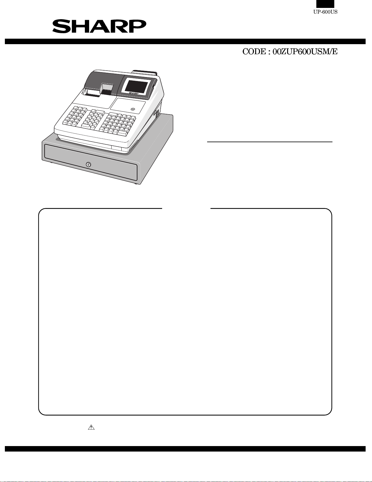
1. APPEARANCE
External view
Front view
Journal cover
Receipt paper
Ribbon cover
Drawer
Drawer lock
Rear view
Validation opening
Printer cover lock
2. RATING
External dimensions :
With a drawer
Weight : With a drawer 16.4kg
Power source 120V AC
Power consumption Stand-by : 16 W
Working temperatures 0 to 40 °C
445 (W) x 485 (D) x 312 (H) mm
10%, 60Hz
Operating : 57 W (max.)
3. KEYBOARD
1) STANDARD KEYBOARD LAYOUT
PRICE
CHANGE
5
4
3
2
1
10
9
8
7
6
MISC
FUNC
CONV
#
TAX
RFND
CANCEL
TAX
SHIFT
VOID
RCPT
PAGE
UP
PAGE
DOWN
ENTER
#/TM
CASH
@
FOR
7
4
1
#
0
PLU/UPC
CL
89
56
2
3
00
Customer display
(Pop-up type)
Operator display
Contrast control
Power switch
Mode switch
Keyboard
AMT
INQ
SHIFT
15
20
TEND
14
19
13
18
12
11
MDSE
17
16
AUTO
FS
FS
AUTO
NEXT
NS
CHK#CH
SBTL
CA/AT
SBTL
2) KEY TOP NAME
Standard key top
KEY TOP DESCRIPTION
0-9,00 Numeric keys
Decimal Point key
CL Clear key
@/FOR Multiplication key
RECEIPT
JOURNAL
PAGE UP Page up key
PAGE DOWN Page down key
CANCEL Cancel key
ENTER Enter key
RFND Refund Key
RCPT Receipt print Key
TAX SHIFT Tax 1 shift key
VOID Void Key
PLU/UPC PLU/UPC code entry key
AUTO1, 2 Automatic sequencing 1 and 2 keys
MISC FUNC Miscellaneous function key
CONV# Currency conversion menu key
CHK# Check Menu Key
CH# Charge Menu Key
SBTL Subtotal Key
CA/AT Cash / amount tendered key
(Dept) 1 to 22 Department 1 to 22 Keys
CASH# Cashier number entry
FS SHIFT Food stamp shift key
FS TEND Food stamp tender key
NS No sale key
TAX Manual tax key
NEXT $ Next higher dollar key
MDSE SBTL Merchandise subtotal key
AMT Amount entry key
#/TM Non-add code/Date & Time display key
INQ Inquiry key
1
2
$
#
PRICE CHANGE UPC price change key
Receipt paper feed key
Journal paper feed key
Cursor keys
Page 3
- - - - - - - - - - - - - - - - - - - - - - - - - - - - - - - - - - - - - - - - - - - - - - - - - - - - - - -
Optional key top
KEY TOP DESCRIPTION
000 Numeric Key
(D-PLU) 1 to 123 Direct PLU 1 to 123 Keys
(Dept) 21 to 99 Department 21 to 99 Keys
%1 to 5 Percent 1 to 5 keys
(-)1 to 5 Discount 1 to 5 keys
CH1 to 9 Charge 1 to 9 keys
CASH MENU Cash menu key
FUNC. MENU Function menu key
RP SEND Remote printer send key
GRT EX Gratuity exempt key
CA2 to 5 Cash 2 to 5 keys
CONV1 to 4 Conversion 1 to 4 keys
RA1 to 2 Received-on-Account 1 and 2 keys
PO1 to 2 Paid out key 1 and 2 keys
AUTO3 to 25 Automatic sequencing 3 and 25 keys
CHK1 to 5 Check 1 to 5 keys
P1 to 6 Price level shift 1 to 6 keys
LEVEL1 to 5 Menu level shift 1 to 5 keys
GD1 to 3 SHIFT Group discount shift 1 to 3 keys
CASH TIP Cash tip key
CHARGE TIP Charge tip key
TIP PAID Tip paid key
EAT IN1 to 3 Eat in 1 to 3 keys
TAX2 to 4 SHIFT Tax 2 to 4 shift keys
SCALE Scale e n try key
OPEN TARE Tare entry key
BAL Balance ke y
DEPOSIT Deposit key
DEPOSIT RF Deposit refund key
DEPT# Department number key
BACK SPACE Back space key
TRANS OUT Transfer out key
TRANS IN Transfer in key
RCP SW Receipt ON/OFF key
WASTE Waste mode key
BS Bill separation key
BT Bill totalize / bill transfer key (CHECK-ADD)
PRINT Val idation print key
BILL Bill print key
PAST VOID Past void key
SBTL VOID Subtotal void key
GDSC %1 to %3 Group discount %1 to 3 keys
COVER CNT Cover count key
N.C New check key
KEY TOP DESCRIPTION
C_NEXT Condiments next key
EDIT TIP Edit tip key
RP ROUND Repeat round key
PLU MENU1 to 50 PLU menu 1 to 50 keys
MACRO1 to 4 Macro 1 to 4 keys
UPSIZE Upsize key
CAP.1 to 10 Data capture 1 to 10 keys
GLU RECALL Table # recall key
MSG1 to 5 Message 1 to 5 keys
MSG# Message menu Key
DELETE Delete key
TRAY SBTL Tray subtotal key
RTN Return key
GAS SBTL Gasoline sales subtotal key
REPEAT Repeat key
IND. PAYMENT Individual payment key
CUST Customer code entry key
BIRTH Birthday entry key
TABLE # Table no. (seat no.) entry key
VOID MENU Void menu key
RFND SALE Refund sale key
P-SHIFT# Price shift menu key
FINAL Tentative finalization key
LEVEL# PLU level shift menu key
SRVC Service key
GLU Guest Look-up key
Page 4
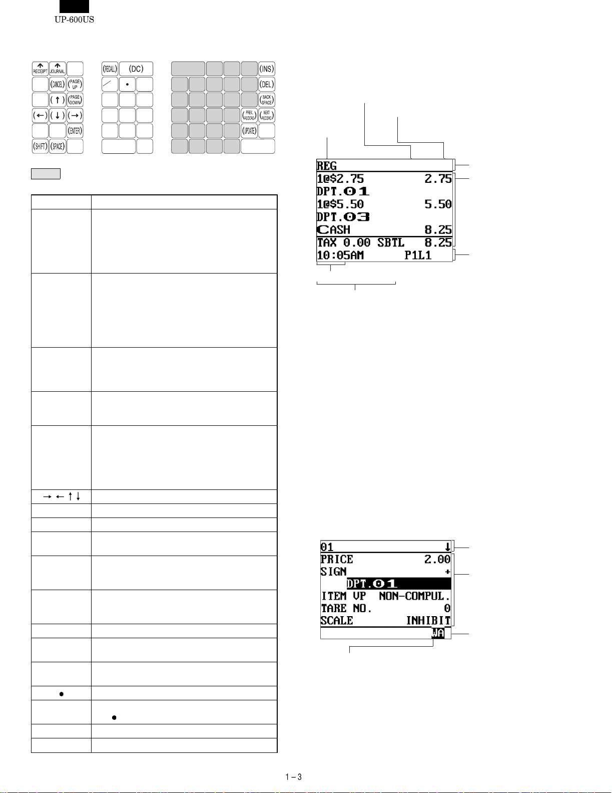
3) PROGRAMMING KEY LAYOUT
3. DISPLAY
A
L
R
X
@
FOR
7
4
1
89
56
2
0
CL
00
G
B
C
D
3
E
F
M
S
Y
H
N
I
O
J
P
K
Q
Z
T
U
V
CA/AT
W
: The shaded area contains the character keys which are
used for programming characters.
KEY TOP DESCRIPTION
SHIFT Used for programming characters.
Entering upper-case letters
You can enter an upper-case letter by using this
key. Press this key just before you enter the
upper-case letter. You should press this key each
time you enter an upper-case letter.
DC Used for programming characters.
Entering double-size characters
This key toggles the double-size character mode
and the normal-size character mode. The default
is the normal-size character mode. When the
double-size character mode is selected, the letter
"W" appears at the bottom of the display.
INS Used for programming characters.
To select a text editing mode
Toggles between the insert mode ("_") and the
overwrite mode ("■").
DEL Used for programming characters.
To delete a character or figure
Deletes a character or figure in the cursor position.
BACK SPACE Used for programming characters.
To delete a character or figure
Backs up the cursor for deleting the character or
figure at the left of the cursor. When your POS
terminal is in the insert mode, this key deletes the
character or the value at the cursor position.
Used to move the cursor.
ENTER Used to program each setting.
TL Used to finalize programming.
CANCEL Used to cancel programming and to get back to
the previous screen.
PREV
RECORD
Used to go back to the previous record, e.g. from
the department 2 programming window back to
the department 1 programming window.
NEXT
RECORD
Used to go to the next record, for example, in
order to program unit prices for sequential
departments.
PAGE DOWN Used to scroll the window to go to the next page.
PAGE UP Used to scroll the window to go back to the
previous page.
CL Used to clear the last setting you have
programmed or clear the error state.
Used to toggle between two or more options.
SBTL Used to list those options which you can toggle by
] key.
the [
RECALL Used to call up a desired code.
Numeric keys Used for entering figures.
SBTL
1) OPERATOR DISPLAY
•
Screen example 1 (REG mode)
Server code
Scroll guidance:
Mode name
Time
Numeric entry
Price level shift indicator
(P1-P6)
PLU level shift indicator
(L1-L5)
When a transaction information
occupies more than 5 lines, scroll
key(s) appears to indicate you can
scroll to the direction.
Status area 1:
Sales information
area:
Sales information
you have just entered
such as items and
prices will appear
between 2nd line and
6th line.
Total is always appear
at 7th line.
Status area 2:
: Shows the PLU/UPC price level
currently selected.
: Shows the PLU level currently se-
lected.
Receipt shift indicator (r) : Shows the receipt shift status.
Stock alarm indicator ( ! ) : Appears when the stock of the PLU
which you entered is zero, negative
or reaches the minimum stock.
Electronic message indicator (M)
Receipt ON/OFF status indicator (R)
: Appears when an electronic mail is
received. (Status 1 area)
: Appears when the receipt ON-OFF
function signs OFF.
Sentinel mark (X) : Appears in the lower right corner of
the screen when the cash in drawer
exceeds a programmed sentinel
amount.
The sentinel check is performed for
the total cash in drawer.
• Screen example 2 (PGM mode)
Programming item
information area
Programming area:
Programmable items
are listed.
Caps lock indicator
(A/a):
Double-size character mode
indicator (W):
Appears when the double-size
character mode is
selected during text programming.
The upper-case letter “A”
appears when caps lock is on,
and the lower-case letter “a”
appears when caps lock is off
during text programming.
Page 5
Screen save mod e
When you want to save the electric power or save the display’s life,
use the screen save function. This function can turn the LCD off when
a server does not operate the POS terminal for an extended period of
time. You can program the time for which your POS terminal should
keep the normal status (in which the backlight is "ON") before it goes
into the screen save mode.
To go back to the normal mode, press any key.
Device type LCD display
Dot format 320(W) x 240(H) Full dot
Dot size 0.24 (W) x 0.21 (H) mm
Dot space 0.02 mm
Dot color White
Back color Dark blue
2) DISPLAY ADJUSTMENT (OPERATION DISPLAY)
You can adjust the contrast of the display by using the contrast
control, and also you can adjust the display angle. Pull up t he tab, the
display will head up.
Tab
Contrast control
Turning the control backwards
darkens the display and
turning it forwards lightens the
display.
The backlight in the display is a consumable part.
When the LCD display may no longer be adjusted and becomes
darker, you should change the backlight.
3) CUSTOMER DISPLAY (Pop-up-type)
• Manager key (MA)
• Operator key (OP)
MA
OP
• Submanager key (SM)
SM
• Service key (SRV)
SRV
The mode switch has these settings:
OFF: This mode locks all register operations.
No change occurs to register data.
OP X/Z: This setting allows cashiers/clerks to take X or Z reports for
their sales information. (This setting may be used only
when your register has been programmed for "OP X/Z
mode available" in the PGM2 mode.)
REG: For entering sales
PGM1: To program those items that need to be changed often:
e.g., unit prices of departments, PLUs or UPCs, and percentages
PGM2: To program all PGM1 items and those items that do not
require frequent changes: e.g., date, time, or a variety of
register functions
MGR: For manager’s and submanager’s entries
The manager can use this mode to make entries that are
not permitted to be made by cashiers/servers -for example,
after-transaction voiding and override entry.
X1/Z1: To take the X/Z report for various daily totals
X2/Z2: To take the X/Z report for various periodic (weekly or
monthly) consolidation
4. KEYS AND SWITCHES
1) MODE SWITCH AND MODE KEYS
MA
SM
X / Z
1
2
REG
MGR
X
1/Z1
X2/Z
2
OP
OFF
PGM
PGM
2) DRAWER LOCK KEY
This key locks and unlocks the drawer. To lock it, turn 90 degrees
counterclockwise. To unlock it, turn 90 degrees clockwise.
SK1-2
4) PRINTER COVER LOCK KEY
This key locks and unlocks the printer cover. To lock it, turn 90
degrees counterclockwise. To unlock, turn 90 degrees clockwise.
Page 6
5. PRINTER (DP-750)
1) SPECIFICATIONS
Part number: DP-750
•
• No. of stations: 2
• Printing system: Mechanical serial dot
• Direction of printing: Bidirectional
• Printing capacity: Receipt – 24 characters
Journal – 24 characters
Validation – 55 characters (one line only)
• Character size: 1.36 (W) 2.75 (H) mm at 7 7 dots
Print pitch:
Column distance 1.59 mm
Row distance 4.23 mm
• Total number of dots: Receipt – 108 dots/216 positions
Journal – 108 dots/216 positions
Validation – 248 dots/495 positions
• Font: 7 7 dots (including half dot)
Space between characters – 1 dot (2 positions)
• Distance between dots: 0.353 mm (H) 0.353 mm (W)
• Print speed: Approx. 3.0 lines/sec.
• Paper feed speed: Receipt – Approx. 30 lines/sec.
Journal – Approx. 30 lines/sec.
• Reliability: MCBF – 4 million lines (excluding the
print head)
Head life – 50 million characters (at 4
dots/1 character/1 pin)
• Validation form sensor: Not available
2) PRINTING AREA
Receipt/journal
87.08
3.56 3.56 3.56
37.87
4.2
44.5± 0.5
RECEIPT JOURNAL
Fig. 5-1
37.87
44.5± 0.5
3.56
Unit : mm
3) PAPER
•
Paper roll dimensions: 44.5 0.5mm in width, 83mm in diameter
• Paper quality: Journal/ Receipt
Bond paper (paper thickness: 0.06 to
0.09mm, paper weight: 52.3 to 64g/m
Validation form
Thickness: 0.07 to 0.14mm
Size:130mm or more (W)
70mm or more (H)
4) INKING
•
Ink supply system: Ink ribbon
• Form: Cartridge/Endless ribbon
• Specification: Material – Nylon
• Ribbon life: Approx. 6 million characters
• Print color: Purple
5) LOGO STAMP : None
6) CUTTER
• Method: Manual
6. DRAWER
1) SPECIFICATION
(1) Drawer box and drawer
Model name SK-460
Size 445 (W) x 464 (L) x 118 (H)
Color GRAY 368
Material Metal
Bell —
Release lever Standard equipment; Front key
Drawer open sensor Standard equipment
2) MONEY CASE
U version A version
Separation from the drawer
Allowed
Separation of the coin
compartments from the money case
Bill separator No Standard (1 pcs)
Number of compartments 7B/5C 4B/8C
Allowed Allowed
Disallowed Disallowed
Bill separator
2
)
Validation form
70
87.0 (PRINT AREA)
130
Fig. 5-2
20
22
Unit : mm
3) LOCK
Location of the lock Front
Method of locking
and unlocking
Key No. SK1-2
Locking: Insert the drawer lock key into
Unlocking: Insert the drawer lock key into
A version : 4B/8CU version : 7B/5C
the lock and turn it 90 degrees
counterclockwise.
the lock and turn it 90 degrees
clockwise.
Page 7
7. RS232 INTERFACE
This machine has two RS232 standard ports for communication to PC, Hand scanner (ER-A6HS1) and etc.
1) PORT 1 (CH1) (CN402)
Connector type: D-SUB 9pin
Data rate: max. 38,400 bps
/CD
1
2
RD
3
SD
/ER
4
5
GND
/DR
6
/RS
7
/CS
8
VCC(+5V)
/CI
S401
2) PORT2 (CH2) (CN403)
Connector type: Modular jack RJ45 8pin
Data rate: max. 115,200 bps
/RS
1
2
/ER
3
SD
4
5
GND
RD
6
/DR
7
/CS
8
CD
S404
S403
GND
CI
VCC
(+5V)
9
3) OPTIONAL DEVICES THAT CAN BE CONNECTED
Standard port Option port (ER-A5RS)
Port No. Port1: CH1 Port2: CH2 Port3: Port4:
Type D-SUB 9pin Moduler RJ45 D-SUB 9pin D-SUB 9pin
CI/+5V selectable
ER-A6HS1 (+5V necessary)
Scanner (+5V not necessary)
Modem –
PC
Printer, Scale
POS utility, 02fd.exe – ––
–––
–––
The ER-A6HS1 cannot be connected to port 2, 3 and 4 because it
requires +5V.
The modem cannot be connected to port 2 because it uses a
different signal line.
For the modular RJ45 to D-Sub 9pin conversion cable, see the
following.
Moduler RJ45 D-sub 9pin
S404
S403
CI
VCC
(+5V)
/RS
/ER
SD
GND
RD
/DR
/CS
/RS
1
2
3
4
5
6
7
8
(Open)
7
4
/ER
3
SD
/CD
1
5
GND
RD
2
/RS
6
/CS
8
/CI
9
CD
GND
Page 8
Page 9
Symbol/PartsCod)
- - - - - - - - - - - - - - - - - - - - - - - - - - - - - - - - - - - - - - - - - - - - - - - - - - - - - - -
2. SALES OPTIONS
No. CLASSIFICATION COMPONENT NAME MODEL NAME REMARK
1 Memory Expansion RAM board UP-S02MB 2M bytes PS-RAM board
UP-S04MB 4M bytes PS-RAM board
2 Display Remote display (Pole type) UP-P16DP 11-Dig.7-Seg. + 16-Dig.Dot
3 Drawer Remote drawer ER-03DW 7B/5C coin case
ER-04DW 5B/5C coin case
4 On-line function RS232 I/F board ER-A5RS 2 ports RS232 I/F
5 Card reader MCR (Magnetic Card Reader) UP-E13MR ISO Type 1 : 3 stripe card
6 Scanner Bar code hand scanner ER-A6HS1
7 Expansion key kit Key top kit ER-11KT7 1
ER-12KT7 1
ER-22KT7 2
Dummy key kit ER-11DK7G 1
ER-51DK7G 5
1 Key top kit
2 Key top kit
2 Key top kit
1 Dummy key kit
1 Dummy key kit
3. LOCAL PURCHASE OPTIONS
No. COMPONENT NAME MODEL NAME REMARK
1 External printers TM-T88/85, TM-T88 (2), TM-T80
2 Slip printer TM-295
3Scale I/F
4 Coin dispenser
5 Color kitchen monitor
6 CAT terminal
1: Please consult with your Sharp regional sales manager.
TM-U200, TM-300
4. SERVI C E OP TIO N S
No. NAME PARTS CODE PRICE DESCRIPTION
1 Mode key grip cover
2 Drip proof mode switch cover
3 Drip proof keyboard cover
4 Text preset keyboard cover
AX For MA key only
BA
BF
BH
5. SERVICE TOOLS
No. NAME PARTS CODE PRICE DESCRIPTION
1 Service key
2 RS232 Loop Back Connector
3 RS232 modular Loop Back Connector
4 Expansion PWB for option board
5 MCR test card
6 Key top remover
7 Key top inst. Jig
AF
BC For RS232 D-SUB 9pin connector
BC For RS232 RJ45 Modular jack connector
BU Fo r ER-A5 RS
BL For UP-E13MR
AX
BB For 2 2 key top
6. SUPPLIES
No. NAME PARTS CODE PRICE DESCRIPTION
1 Roll paper
2 Ink libbon
AR 5 roll/pack
AZ Purple
Page 10
7. HOW TO USE SERVICE TOOLS
1) EXPANSION PWB : CKOG-6708RCZZ
•
External view
Purpose 1 : Used f or servicing and repairing of options (such as the
ER-A5RS) which are connected with the main body option connector.
[Procedure 1]
Use an insulator base as shown in the shaded section when performing servicing.
Main PWB
UP-600
Expansion PWB
(CKOG-6708RCZZ)
ER-A5RS
PWB
A
Loop back connectors
UKOG-6705RCZZ
Base
2) MCR TEST CARD : UKOG-2357RCZZ
•
Used when executing the diagnostics of the UP-E13MR.
• External view
To check the option I/F PWB from the solder side, connect the I/ F
PWB to OPTCN2. To check from the parts side, connect to OPTCN3.
(Note) The option I/F PWB should be held horizontally so that no
excessive stress is applied to connecting section
.
[Procedure 2]
Pop up
String
UP-600
Expansion PWB
Main PWB
Control ROM
(CKOG-6708RCZZ)
ER-A5RS
PWB
Put a string between the pop up and the option PWB. Adjust the
length of the string so that the CKOG-6708RCZZ and the option PWB
are not binding. Once verified, then you may proceed with performing
service.
Loop back connectors
UKOG-6705RCZZ
Page 11
CHAPTER 3. SERVICE PRECAUTION
1. IPL (Initial Program Loading) FUNCTION
1) INTRODUCTION
The application software of the UP-600 is written in the flash ROM.
In the following cases, writing of the application software into the flash
ROM is required.
• When the flash ROM is replaced with a new one. The service part
flash ROM does not include the application software in it.
• When IPL writing is required because of a change in the software.
The service part of the main PWB unit includes the flash ROM with
the application software written in it, and there is no need for
writing the application software when replacing the main PWB unit.
2) IPL PROCEDURE
There are two ways for the IPL procedures.
• IPL from P-ROM
• IPL from PC communication (Please refer to the next section)
The detailed descriptions on the above procedures are given below.
3) IPL FROM P-ROM
Master ROM-1 : VHI27801RAS1A
Master ROM-2 : VHI27801RAT1A
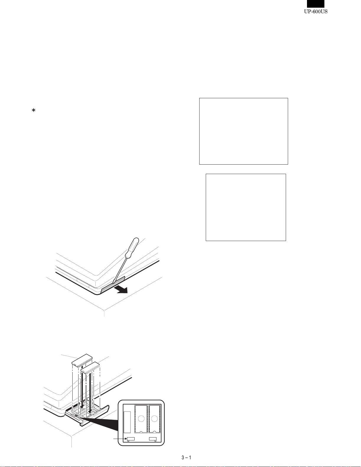
Before installation, turn off the power switch on the UP-600 and unplug the AC cord from the AC outlet.
1. Insert a screwdriver into the sl it on the right side of the lower
cabinet to remove the option RAM case.
4. Place the mode key to any position except OFF or SRV’.
5. Turn on the power switch of the UP-600.
6. The following display is shown and the IPL procedure is started.
When the procedure is completed, the message of "Completed"
is shown.
IPL from PROM
Version check…
Erase …
IPL write start
26 27 28 29 2A 2B
2C 2D 2E 2F 30 31
32 33 34 35 36 37
38 39 3A 3B 3C 3D
3E 3F
Verify …
Completed.
IPL write completed
2. IPL switch (SW301) on the IPL ROM PWB: Set the IPL switch
(SW301) to the ON position.
3. Install the ROMs into the IC sockets on the IPL ROM PWB as
shown below.
ROM1 ROM2
7. Turn off the power switch of UP-600.
8. Remove to the ROMs from the IPL ROM PWB.
9. IPL switch (SW301) on the IPL ROM PWB: Set the IPL switch
(SW301) to the OFF position.
10. Perform one of the master reset procedures.
SW301
ROM1 ROM2
on off
Page 12
Symbol/PartsCod)
- - - - - - - - - - - - - - - - - - - - - - - - - - - - - - - - - - - - - - - - - - - - - - - - - - - - - - -
2. UP-600 UTILITY TOOLS
1) OUTLINE
This Specification document describes the explanation about " POSUTILITYTOOL.EXE and "02FD.EXE".
"POSUTILITYTOOL.EXE"and "02FD.EXE" works on Windows 95/98
of PC and they have the following
Functions by connecting UP-600 with RS232.
POSUTILITYTOOL.EXE : IPL of UP-600 Program Object
02FD.EXE : All RAM Data Upload/Download
(PC software tool instead of the current ER-02FD.)
3) PROCEDURE
3) -1. POS UTILITY
2) CONNECTION
PC and UP-600 are connected by RS232.
Connect the CH2 port of the UP-600 t o the RS-232 interface of the
PC.
CI
VCC
(+5V)
S404
S403
UP-600:CH2
CD
GND
PC
D-SUB 9pin - D-SUB 9pin
cable
RS232 Cable Connecting:
[PC]
D-sub 9pin
7
4
3
SD
1
5
GND
2
RD
6
8
9
D-sub 9pin
/RS
7
/ER
4
3
/CD
1
GND
5
2
/DR
6
/CS
8
/CI
9
D-SUB 9pin - modular RJ-45
conversion cable
[UP-600]
(Open)
Moduler RJ45
/RS
1
/ER
2
SD
3
4
GND
5
RD
6
/DR
7
/CS
8
7
4
3
SD
1
5
2
RD
6
8
9
No Procedure on P.C. side No Procedure on UP-600 side
1 Install the "POSUTILITYTOOL.EXE" on the P.C.
2 Turn OFF the power.
3 Select "IPL Mode".
Set the "IPL Switch" (SW302) of the UP-600 to "ON".
on off
4 Turn ON the power.
5 Starting of "IPL Mode".
The UP-600 displays
"IPL from Serial I/O"
IPL from Serial I/O
on off
SW302
6 Connect the P.C. and the UP-600 (CH2) via RS232. (Fig 1)
Page 13
No Procedure on P.C. side No Procedure on UP-600 side
7 Execute the "POSUTILITUTOOL.EXE" on the P.C.
*Please close all other applications while using this utility.
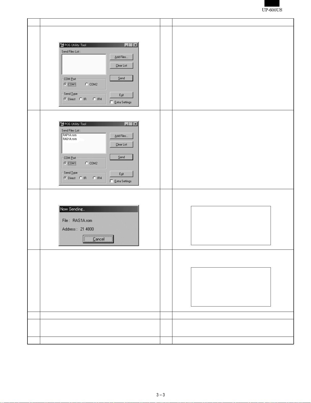
8 Select the ROM object Files by clicking the "Add Files.." button.
9 Push the "SEND" button.
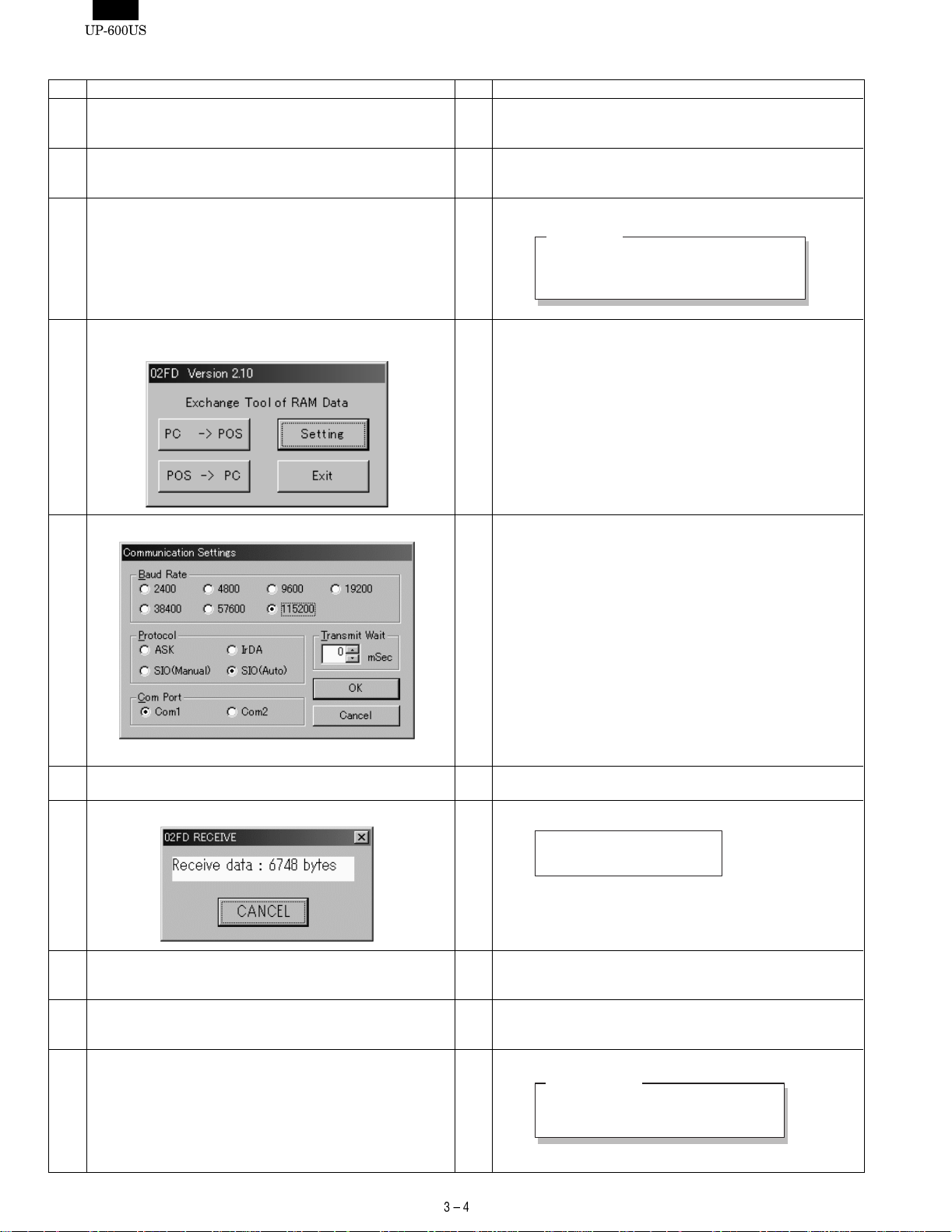
Program data is sent to the UP-600 automatically.
10 When data sending is completed,
the initial Window is shown after "Complete" window.
Program data is received from the P.C. automatically.
9
The UP-600 displays.
IPL from Serial I/O
Connected IRDA 115200
21 22 23 24 25 26 27 28
The UP-600 displays
10
"Completed."
IPL from Serial I/O
Connected IRDA 115200
21 22 23 24 25 26 27 28
29 2A 2B 2C 2D 2E 2F
Completed.
IPL from Serial I/O
Connected IRDA 115200
30 31 32 33 34 35 36 37
38 39 3A 3B 3C 3D 3E 3F
Completed.
11 Turn OFF the power.
Select "Normal Mode".
12
Set the "IPL swit ch" to "OFF".
(Ref. Hardware manual)
13 Execute the "Service Reset" on UP-600.
Page 14
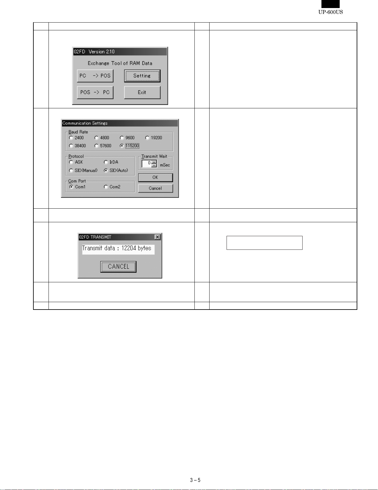
3) -2. 02FD
No Procedure on P.C. side No Procedure on UP-600 side
1 Install the "02FD.EXE" on the P.C.
ALL RAM Data UpLoad : Go to "2"
ALL RAM Data DownLoad : Go to "9"
2 ALL RAM Data UpLoad
Connect the P.C. and the UP-600 (CH2) via RS232. (Fig 1)
4 Execute the "02FD.EXE" on the P.C.
*Please close all other applications while using this utility.
2 Enter the SRV mode.
Select " 2 SETTING ".
Select " 14 BACKUP SEND"
3 The UP-600 displays
BACKUP SEND
SEND DATA ALL RAM
SPEED PROGRAMMED SPEED
5 Set the Communication method by pushing the "Setting" Button.
Push the "OK" Button.
6 Push the "Receive Start" Button.
And Select the Receiving File.
7 Communication starts. 7 Push CA/AT key. The UP-600 displays
SENDING 00000
8 The UpLoad is completed.
The initial Window is shown.
8 The UpLoad is completed.
The SETTING menu is shown.
Push the "Exit" Button.
9 ALL RAM Data UpLoad
Connect the P.C. and the UP-600 (CH2) via RS232. (Fig 1)
9 Enter the SRV mode.
Select " 2 SETTING".
Select " 15 BACKUP RECEIVE"
10 The UP-600 displays
BACKUP RECEIVE
SPEED PROGRAMMED SPEED
Push the CA/AT key.
Page 15
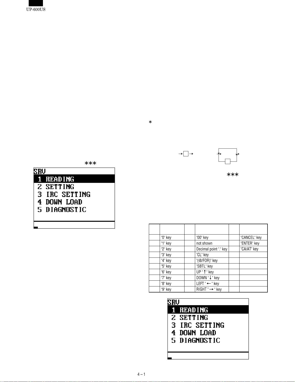
No Procedure on P.C. side No Procedure on UP-600 side
11 Execute the "02FD.EXE" on the P.C.
*Please close all other applications while using this utility.
12 Set the Communication method by pushing the "Setting" Button.
Push The "OK" Button.
13 Push the "Transmit Start" Button.
And Select the Sending File.
14 Communication starts. 14 The UP-600 displays
15 The DownLoad is completed.
The initial Window is shown.
Push the "Exit" Button.
3. NOTE FOR HANDLING OF LCD
• The LCD elements are made of glass. Use extreme care when
handling the LCD.
Any strong shock applied to the LCD can cause damage.
• If the LCD element is broken and the liquid has leaked, do not
come in contact with it. If the liquid is attached to your skin or cloth,
immediately clean with soap.
• Use the unit under the rated conditions to prevent against damage.
• Be careful not to drop water or other liquids on the display surface.
• The reflection plate and the polarizing plate are easily scratched.
Be careful not to touch them with hard objects such as glass,
tweezers, etc. Never hit, push, or rub the surface with hard objects.
• When installing t he unit, be careful not t o apply stress to the LCD
module. If excessive stress is applied, abnormal display or uneven
color may result.
RECEIVING 00000
15 The DownLoad is completed.
The SETTING menu is shown.
16 Execute the " Service Reset " on the UP-600
Page 16
CHAPTER 4. SRV. RESET AND MASTER RESET
The SRV key is used for operating in the SRV mode.
1. SRV. RESET (Program Loop Reset)
Procedure
• Method 1
1) Turn off the AC switch.
2) Set the mode switch to (SRV’) position.
3) Turn on the AC switch.
4) Turn to (SRV) position from (SRV’) position.
• Method 2
1) Set the mode switch to PGM2 position.
2) Turn off the AC switch.
3) While holding down the JOURNAL FEED and RECEIPT FEED
keys, turn on the AC switch.
Note: When disassembling and reassembling always power up us-
ing method 1 only. Method 2 will not reset the CKDC9.
Note: SRV programming job#926-B must be set to a "4" to allow the
PGM program loop reset.
PRG. RESET
MRS-2 (Master resetting 2)
Used to clear all memory and keyboard contents.
This reset returns all programming back to defaults. The keyboard
must be entered by hand.
This reset is used if an application needs a different keyboard layout
other than that supplied by a normal MRS-1.
Procedure
1) Turn off the AC switch.
2) Set the MODE switch to the (SRV’) position.
3) Turn on the AC switch.
4) While holding down the JOURNAL FEED and RECEIPT FEED
keys, turn to the (SRV) position from the (SRV’) position.
5) Key position assignment:
After the execution of a MRS-2, only the RECEIPT FEED and
JOURNAL FEED keys can remain effective on key assignment.
Any key can be assigned on any key position on the main keyboard.
[key setup procedure]
0
Disable
*2
Free key setup
complete.
*1
MRS-2 executed Key position set Free key
0
2. MASTER RESET (All memory clea r)
There are three possible methods to perform a master reset.
MRS-1 (Master resetting 1)
Used to clear all memory contents and return the machine back to its
initial setting s .
Returns the keyboard to the default layout.
Procedure
1) Turn off the AC switch.
2) Set the MODE switch to the (SRV’) position.
3) Turn on the AC switch.
4) While holding down the JOURNAL FEED key, turn to the
(SRV) position from the (SRV’) position.
MASTER RESET
NOTES:
*1: When the 0 key is pressed, t he key of the key number on the
display is disabled.
*2: Push the key on the position to be assigned. With this, the key of
the key number on the display is assigned to that key position.
*3: When relocating the keyboard, the PGM 1/2 modes use the
standard key layout.
Key
No.
001
002 012 022
003 013 023
004 014
005 015
006 016
007 017
008 018
009 019
010 020
Key
name
Key
No.
011 021
Key
name
Key
No.
Key
name
Page 17
Symbol/PartsCod)
- - - - - - - - - - - - - - - - - - - - - - - - - - - - - - - - - - - - - - - - - - - - - - - - - - - - - - -
MRS-3 (Master resetting 3)
Master resetting 3 requires the entry of Seri al No. data in addition to
Master resetting 2.
After completion of the MRS-3, the following operations and programming will be inhibited.
1. GT programming.
2. All memory download via RS-232.
3. GT resets with Z report. (Z report can be made, but the GT will not
be reset.)
Procedure
1) Turn off the AC switch.
2) Set the reset switch to the "SRV" position.
3) Turn on the AC switch.
4) While holding down the JOURNAL FEED key and MRS-3 key,
turn to the (SRV) position from the (SRV’) position.
MRS-3 key : UP-600=[CANCEL] key
UP-700=[PLU72] key
5) The product serial No. input window is displayed as shown
below.
DISPLAY:
SERIAL No. 00000000
Enter the product serial No. of this POS and enter the [CA/AT]
key.
6) Key position assignment:
After the execution of MRS-3, only the RECEIPT FEED and
JOURNAL FEED keys can remain effective on key assignment.
Any key can be assigned on any key position on the main keyboard.
[key setup procedure]
0
Disable
*2
Free key setup
complete.
*1
MRS-2 executed Key position set Free key
0
MASTER RESET
NOTES:
*1: When the 0 key is pressed, t he key of the key number on the
display is disabled.
*2: Push the key on the position to be assigned. With this, the key of
the key number on the display is assigned to that key position.
*3: When relocating the keyboard, the PGM 1/2 modes the use
standard key layout.
Key
No.
001
002 012 022
003 013 023
004 014
005 015
006 016
007 017
008 018
009 019
010 020
Key
name
Key
No.
Key
name
Key
No.
011 021
Key
name
Page 18
CHAPTER 5. DIAGNOSTICS SPECIFICATIONS
1. GENERAL DESCRIPTION
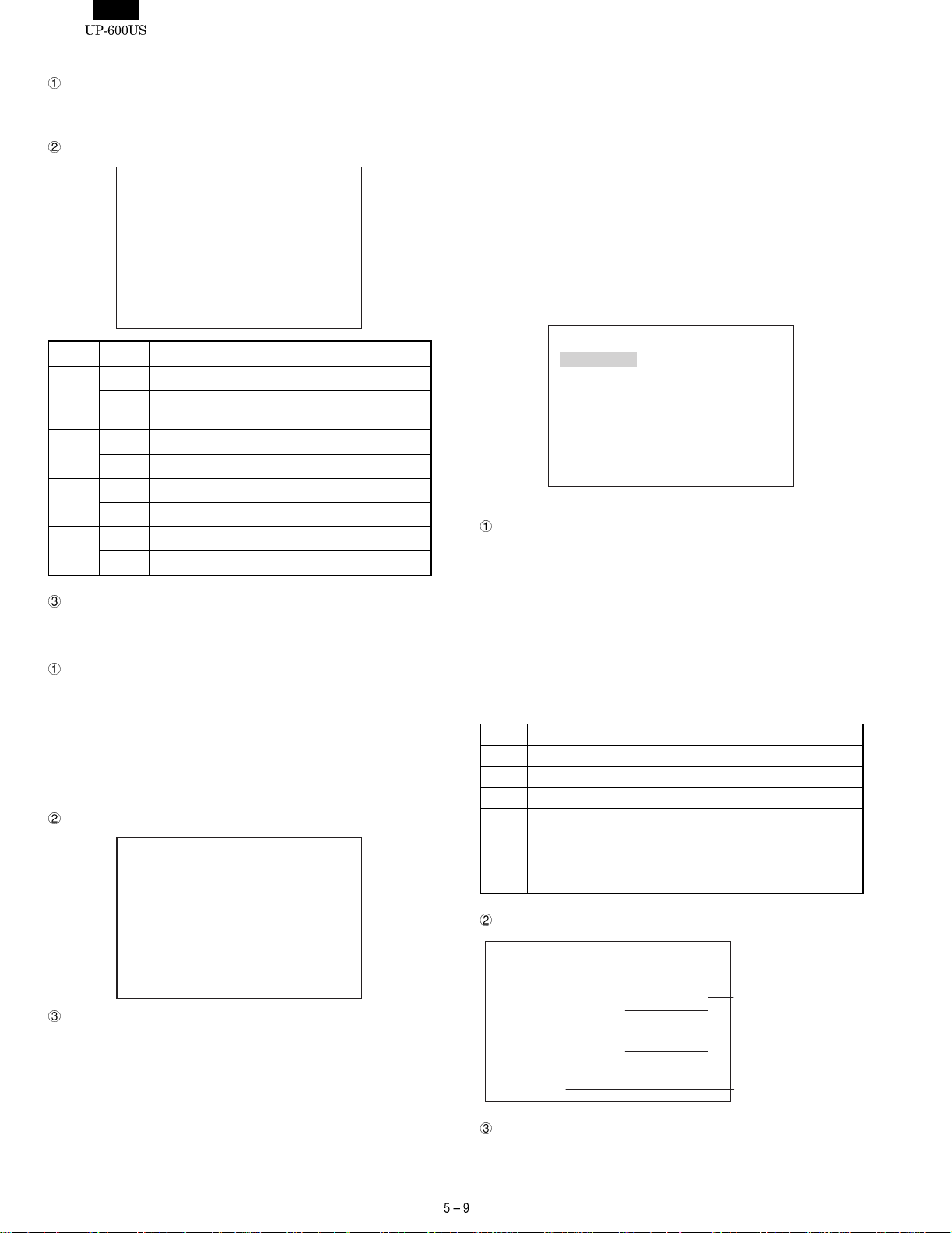
This Diag Program consists of a number of Diag. programs for the
UP-600, which facilitate the PWB check, process check and the operation check of the system during servicing.
The Service Diag. programs are all contained in the standard ROM.
2. SYSTEM COMPOSITION
UP-600 only
UP-600
Fig 2-1. Service
3. DIAG.
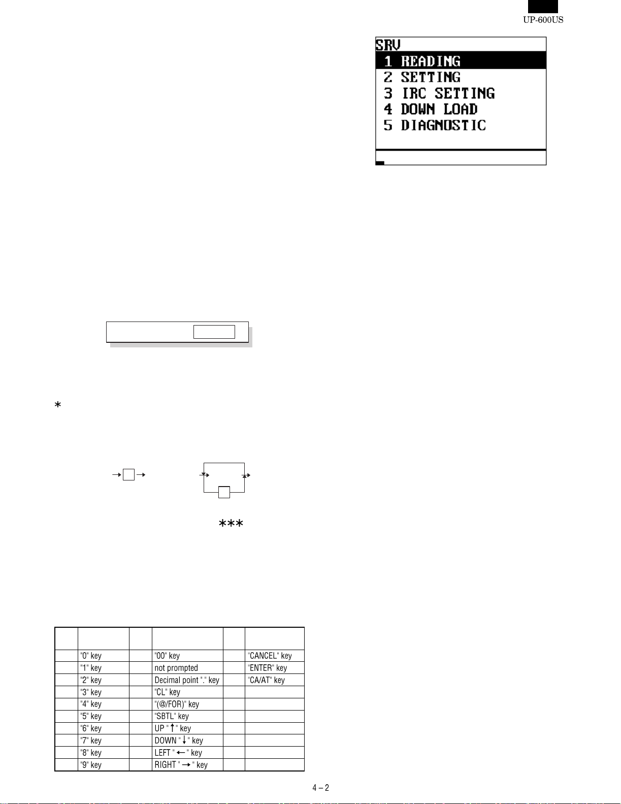
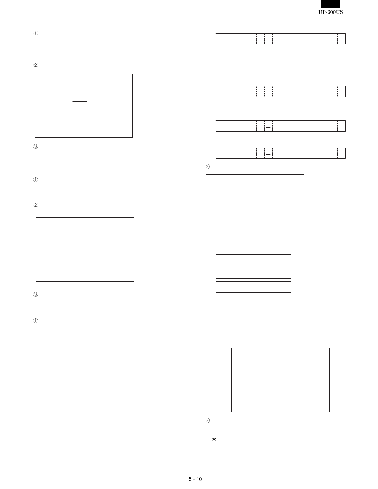
Starting the Diag. Program
The Diag. Program is written on the external ROM, which is executed
by the CPU (H8/510) and runs on the following conditions:
The logic power supply is normal.
(+5V, VCKDC, POFF, +24V)
Both the I/O pins of the CPU and the CPU internal logic are
normal, and the CKDC9 and MPCA9, system bus, and standard
ROM/RAM are normal.
1) EXECUTING DIAG PROGRAM
To start the Diag. Program, enter the SRV mode. Select the option
item DIAGNOSTICS from the MENU using the cursor keys and press
the ENTER key.
The DIAG. MAIN MENU appears on the screen as shown below. The
cursor is displayed in reverse video and can be moved using the
up/down arrow keys. Move the cursor to the menu item you want and
press the ENTER key to execute the corresponding Diag. program.
When each Diag. program is completed, the screen returns to the
DIAG. MAIN MENU. Press the CANCEL key to exit the Diag. Program and the screen returns to the SRV mode menu screen.
UP-600 DIAG V1.0A
PRODUCT&TEST
RAM&ROM&SSP
CLOCK&KEY&SWITCH
SERIAL I/O
DISPLAY&PRINTER
MCR&DRAWER
TCP/IP
2) RAM & ROM & SSP DIAGNOSITCS
This program tests the standard RAM, expanded RAM, standard and
service ROMs, and SSp circuit. RAM&ROM&SSP is selected on the
MAIN MENU, the following sub-menu screen appears. The cursor
shown in reverse video can be moved using the up/down arrow keys.
Move the cursor to the menu item you want and press the ENTER
key to execute the corresponding program. Press the CANCEL key to
return the screen to this submenu.
RAM&ROM&SSP DIAG
Standard RAM Check
UP-S04MB Check
UP-S02MB Check
Standard ROM Check
Service ROM Check
SSP Check
2)-1. Standard RAM check
Checking
The program performs the following checks on the standard
512KB of RAM. Data in memory remains unchanged before and
after the checks.
The following operations are performed for the memory addresses
to be checked (780000H - 7FFFFFH).
PASS1 : Save data in memory
PASS2 : Write data "0000H"
PASS3 : Read and compare data "0000H" and write data "5555H".
PASS4 : Read and compare data "5555H" and write data "AAAAH"
PASS5 : Read and compare data "AAAAH"
PASS6 : Return data into memory
If any comparison is not normal during the check sequence from
PASS 1 through 6, the error message appears.
If any error is not found up to the final address, the sequence
ends normally.
Then, another round of address checks is carried out using the
above check sequence
If an error occurs, the error message appears and the check
stops. The read/write of the address where the error occurs is
repeated.
Check point address = 780000H, 780001H
780002H, 780004H
780008H, 780010H
780020H, 780040H
780080H, 780100H
780200H, 780400H
780800H, 781000H
782000H, 784000H
788000H, 790000H
7A0000H, 7C0000H
Page 19
Symbol/PartsCod)
- - - - - - - - - - - - - - - - - - - - - - - - - - - - - - - - - - - - - - - - - - - - - - - - - - - - - - -
Display
The capacity checked is displayed in units of 64KB.
Standard RAM Check
512KB:PASS!!(or ERROR!!)
Error:XXXXXXH
Write:XXXXH
Read:XXXXH
The error address and bit are displayed only when an error occurs
(They are not displayed if there is no error.)
How to exit the program
You can exit the program by pressing the CANCEL key after the
results are displayed.
2)-2. UP-S02MB Check
Checking
The program checks for the presence of the UP-S02MB in the
following procedure.
Data in memory remains unchanged before and after checking.
i. Write 55AAH in 9FFFFEH.
ii. Read 9FFFFEH and compare the data with 55AAH. If both
data are correct and BFFFFEH is the same as 55AAH, the
following tests are performed. If not correct, the message
"0KB: ERROR!!" appears and checking ends.
The following checks are performed on the UP-S02MB.
The following operations are performed for the address space to
be checked (800000H - 9FFFFFH).
PASS1 : Save data in memory.
PASS2 : Write data "0000H".
PASS3 : Read and compare data "0000H" and write data "5555H".
PASS4 : Read and compare data "5555H" and write data "AAAAH".
PASS5 : Read and compare data "AAAAH".
PASS6 : Return data into memory.
If any comparison is not normal during the check sequence from
PASS 1 through 6, the error message appears.
If any error is not found up to the final address, the sequence
ends normally.
Then, another round of address checks is carried out using the
above check sequence.
If an error occurs, the error message appears and the checking
stops. The read/write of the address where the error occurs is
repeated.
Check point address = 800000H, 800001H
800002H, 800004H
800008H, 800010H
800020H, 800040H
800080H, 800100H
800200H, 800400H
800800H, 801000H
802000H, 804000H
808000H, 810000H
820000H, 840000H
880000H, 900000H
Display
The capacity checked is displayed in units of 64KB.
UP-S02MB Check
2048KB:PASS!!(or ERROR!!)
Error:XXXXXXH
Write:XXXXH
Read:XXXXH
The error address and bit are displayed only when an error occurs
(They are not displayed if there is no error.)
How to exit the program
You can exit the program by pressing the CANCEL key after the
results are displayed..
2)-3. UP-S04MB Check
Checking
The program checks for the presence of the UP-S04MB in the
following procedure. Data in memory remains unchanged before
and after checking.
i. After writing 55AAH in BFFFFEH, write AA55H in 9FFFFEH.
ii. Read BFFFFEH and compare the data with 55AAH. Data in
BFFFEH is correct, the following checks are perf ormed. Data
read is AA55H, the message "UP-S02MB!!" appears and the
check ends. If the data read is not either 55AAH or AA55H, the
message "0KB:ERROR!!" appears and the check ends.
The following checks are performed on the UP-S04MB.
The following operations are performed for the address space to
be checked (800000H - BFFFFFH).
PASS1 : Save data in memory.
PASS2 : Write data "0000H".
PASS3 : Read and compare data "0000H" and write data "5555H".
PASS4 : Read and compare data "5555H" and write data "AAAAH".
PASS5 : Read and compare data "AAAAH".
PASS6 : Return data into memory.
If any comparison is not normal during the check sequence from
PASS 1 through 6, the error message appears.
If any error is not found up to the final address, the sequence
ends normally.
Then, another round of address checks is carried out in the above
check sequence.
If an error occurs, the error message appears and the checking
stops. The read/write of the address where the error occurs is
repeated.
Check point address = 800000H, 800001H
800002H, 800004H
800008H, 800010H
800020H, 800040H
800080H, 800100H
800200H, 800400H
800800H, 801000H
802000H, 804000H
808000H, 810000H
820000H, 840000H
880000H, 900000H
A00000H
Page 20
Display
The capacity checked is displayed in units of 64KB.
UP-S04MB Check
4096KB:PASS!!(or ERROR!!)
Error:XXXXXXH
Write:XXXXH
Read:XXXXH
The error address and bit are displayed only when an error occurs
(They are not displayed if there is no error.)
How to exit the program
You can exit the program by pressing the CANCEL key after the
results are displayed.
2)-4. Standard ROM Check
Checking
The standard ROM area (200000H - 3FFFFFH) is added in units
of bytes. When the lowest 2 digits of the result is 20H, it is regarded as normal.
In addition, the ROM version and model name code stored in the
addresses 31FFE0H - 31FFFFH where the ROM version and
checksum correction data are stored are displayed. Data (ASCII)
is stored in the following formats:
31FFE0H~31FFEFH : Model name CODE (Example: "UP-600",
to be displayed until DATA becomes 00H.)
31FFF0H~31FFF9H : 27801R****(****=PROGRAM VERSION)
31FFFAH~31FFFBH : BLOCK NO.("20"~"3F")
31FFFCH : TERMINATOR ("=")
31FFFDH~31FFFEH : BLOCK VERSION (Example: "00")
31FFFFH : CHECK SUM correction DATA
FLASH ROM used as the standard ROM has 64K-byte-unit rewrite BLOCKs. To perform VERSION management in the BLOCK
unit, these BLOCKs have the same 16 byte organizati on as those
after the previous 31FFF0H and arranged every 64KBYTE. At this
time, the checksum for each BLOCK is corrected to be 01H so
that the entire 2MBYTE become a total of 20H.
Regarding the display of the PROGRAM VERSION, the FLASH
write MASTER EPROM has 8Mbits chips to allow management of
the block units of the chip. The PROGRAM VERSION stored in
blocks at 21H and 31H are displayed.
0 PAGE (BLOCK) where the IPL is stored, displays the PROGRAM VERSION of the IPL to make it possible to manage individual programs.
Display
The capacity checked is displayed in units of 64KB.
Service ROM Check
PASS!!(or ERROR!!)
APL: 27801R****
27801R****
IPL:**
JOURNAL print
BLOCK Version.
20=** 21=** 22=** 23=**
24=** 25=** 26=** 27=**
. . . . . . . . . . .
3C=** 3D=** 3E=** 3F=**
How to exit the program
You can exit the program by pressing the CANCEL key after the
result of checking is displayed.
2)-5. SERVICE ROM Check
Checking
The SERVICE ROM area composed of two EPROMs (D00000H -
EFFFFFH) is added in units of bytes for each chip. If the lowest 2
digits are 10H, it is regarded as normal.
In addition, the ROM version and model name code stored in the
addresses D1FFE0H - D1FFFFH where the ROM version and
checksum correction data are stored are displayed. Data (ASCII)
is stored in the following formats:
D1FFE0H~D1FFEFH : Model name CODE(Example: "UP-600",
to be displayed until data is 00H.)
D1FFF0H~D1FFF9H : 27801R****(****=PROGRA M VERS I ON)
D1FFFAH~D1FFFBH : BLOCK NO.("20"~"2F")
D1FFFCH : TERMINATOR("=")
D1FFFDH~D1FFFEH : BLOCK VERSION(Example:"00")
D1FFFFH : CHECK SUM correction DATA
This SERVICE ROM is used to write data into FLASH ROM and if
any error occurs during rewriting of the FLASH ROM, it is not
possible to resume operations. Its configuration is the same as the
standard ROM.
0 PAGE (BLOCK) where the IPL is stored displays the PROGRAM VERSION of the IPL to make it possible to manage individual programs.
Display
The capacity checked is displayed in units of 64KB.
Service ROM Check
ROM1:PASS!!(or ERROR!!)
ROM2:PASS!!(or ERROR!!)
APL: 27801R****
27801R****
IPL:**
JOURNAL print
BLOCK Version.
20=** 21=** 22=** 23=**
24=** 25=** 26=** 27=**
. . . . . . . . . . .
3C=** 3D=** 3E=** 3F=**
How to exit the program
You can exit the program by pressing the CANCEL key after the
result of checking is displayed.
Page 21

2)-6. SSP Check
Checking
When started, this check program automatically sets the test SSP,
performs the SSP check and displays the results.
The SSP check sets check d ata in the empty space in t he SSP
entry register. After checking is completed, only the check data is
erased. Any setting remains intact before and after this check
program is executed.
Display
SSP Check
PASS!!(or ERROR!!)
How to exit the program
You can exit the program by pressing the CANCEL key after the
results are checking is displayed.
3) TIMER & KEYBOARD & CLERK SWITCH
DIAGNOSTICS
This program checks the operation of t he CKDC’s clock crystal, keyboard and tests the clerk switch and mode switch.
You can return to the Diag menu screen by pressing the CANCEL
key.
3)-4. Mode Switch Check
Checking
The mode switch position code is displayed in a hexadecimal
number.
SRV:0, PGM2:1, PGM1:2, OFF:E, OP X/Z:3, REG:4, MGR:5,
X1/Z1:6, X2/Z2:7
Intermediate code:E, Multiple error F
4) RS232 I/F DIAGNOSTICS
The program tests the RS232 interface for the main PWB and the
optional board ER-A5RS. Attach a 9-pin D-sub loop back connector
(UKOG-6717RCZZ) wired as shown in Fig. 3-11, to the port you are
going to test.
1pinCD
2pinRD
3pinSD
4pinER
5pinGND
6pinDR
7pinRS
8pinCS
9pinCI
Fig. 3-11. Wiring diagram of loop back connector (UKOG-6717RCZZ)
The following menu appears on the screen. The cursor shown in
reverse video can be moved using the up/down arrow keys. Move the
cursor to the menu item you want to execute and select by pressing
the Enter key to the corresponding Diag. Program. Press the CANCEL key to return the screen to this submenu.
When setting the channel for the RS232 interface, do not set more
than two ports to the same channel . The UP-600 accommodates up
to one ER-A5RS board, but use caution not to allow each port to
have the same channel; otherwise the hardware might be destroyed.
3)-1. Timer Check
Checking
Check the operation of the CKDC9’s clock crystal.
The area showing "YY/MM/DD & MM:HH" is continuously dis-
played. Check whether the display blinks in black and white every
0.5 seconds and the time shown is updated.
3)-2. Keyboard Check
Checking
The program checks the input through the keyboard of the UP-
600.
A 3-digit position code corresponding to a key pressed appears on
the screen, along with a catch sound.
3)-3. Clerk SW Check (Not for U version)
Checking
The code of the key inserted into t he cl erk key switch appears in a
decimal number.
RS232 I/F DIAG
CH1 Check
CH8 Check
When Diag. is started, the channel check is performed and only the
channels already set appear on screen.
Note: The channel numbers displayed are logical numbers on soft-
ware, In practical terms, CH1 means the CH1 of the rear connector of the POS and CH8 means the CH2 of the rear connector of the POS. If options are installed, only the ones (CH2
- CH7) which have been set will be added and displayed.
4)-1. CHANNEL Check
Checking
The screen shows only the channels for which have been set and
are connected to the ECR. Compare the channels shown on the
screen and the settings of the channel setting DIP SW of the
RS232 interface board.
The RS232 on the main PWB of the UP-600 is fixed to CH1 and
CH8. It is therefore necessary for the ER-A5RS to set the channel
to CH2 - CH7.
(Ref) ER-A5RS channel settings ("1" = SW OFF, "0" = SW ON)
Page 22
ER-A5RS CON3 (RSCN1)
S1-1 S1-2 S1-3 CHANNEL
0 0 0 Disabled
0 0 1 No setting allowed (Standard RS)
0 1 0 CHANNEL 2
0 1 1 CHANNEL 3
1 0 0 CHANNEL 4
1 0 1 CHANNEL 5
1 1 0 CHANNEL 6
1 1 1 CHANNEL 7
ER-A5RS CON4 (RSCN2)
S1-4 S1-5 S1-6 CHANNEL
0 0 0 Disabled
0 0 1 No setting is allowed (Standard RS)
0 1 0 CHANNEL 2
0 1 1 CHANNEL 3
1 0 0 CHANNEL 4
1 0 1 CHANNEL 5
1 1 0 CHANNEL 6
1 1 1 CHANNEL 7
How to exit the program
Press the CANCEL key to exit the program.
4)-2. CH1 Check
Checking
If any channel is not set, the error message (ERROR: CHx) ap-
pears. When the channel is set, the following checks are performed.
i. Control signal check
ERn RSn DRn Cin CDn CSn
OFF OFF OFF OFF OFF OFF
OFF ON OFF OFF ON ON
ON OFF ON ON OFF OFF
ON ON ON ON ON ON
The program performs the read checks of the above inputs and
interrupt checks of CS, CI, and CD.
During the read check, ER and RS are changed over in the above
order, checking the logic of DR, CI, CD and CS.
If the check result does not agree with the logic in the table, the
error message appears. "ON" in the table means active low and
"OFF" means active high.
In the interrupt check, the CS, CI and CD interrupts are permitted
one by one (The mask is canceled.).
The error message appears if an interrupt does not occur when
each signal is active or if an interrupt occurs when each signal is
not active.
Four cycles of the above check is performed.
ii. Data transfer check
As check data, loop back data transfer of 256 bytes of 00H - 0FFH
is performed. The baud rate is 38400 bps.
iii. TIMER CHECK (RS232 ON BOARD TIMER)
Before starting the check ii, perform the RCVDT start of the timer
you want to check and set to 5 ms. Make sure::
• No TRQ- is generated during the implementation of check ii.
• TRQ- is generated at 5 ms after check ii is completed.
Display
RS232 CH1 Check
PASS!!(or ERROR!!)
Details of the errors are printed on the journal.
ERROR
No.
1 ER-DR : ERROR ER-DR LOOP ERROR
2 ER-CI : ERROR ER-CI LOOP ERROR
3 RS-CD : ERROR RS-CD LOOP ERROR
4 RS-CS : ERROR RS-CS LOOP ERROR
5 CI INT : ERROR No CI interrupt occurs.
6 CD INT : ERROR No CD interrupt occurs.
7 CS INT : ERROR No CD interrupt occurs.
8 TXEMP : ERROR TXEMP is not set.
9 TXEMP INT : ERROR TXEMP interrupt does not
10 TXRDY : ERROR TXRDY is not set.
11 TXRDY INT : ERROR TXRDY interrupt does not
12 RCVRDY : ERROR RCVRDY is not set.
13 RCVRDY INT : ERROR RCVRDY interrupt does not
14 SD-RD : ERROR SD-RD LOOP ERROR
15 SD-RD : ERROR SD-RD LOOP ERROR
16 TIMER : ERROR TIMER ERROR
17 TIMER INT : ERROR TRQ1- interrupt does not
How to exit the program
Press the CANCEL key to exit the program.
ERROR print Details of ERROR
occur.
occur.
(Not possible to receive.
TRQ- occurs during the
implementation of check ii.)
occur.
(DATA ERROR)
(DATA ERROR)
(After check ii is completed)
occur.
Page 23
4)-3. CH2 Check
Checking
The procedure for checking, display and the method of exiting the
programs are the same as for the CH1 check.
4)-4. CH3 Check
Checking
The procedure for checking, display and the method of exiting the
program are the same as for the CH1 check.
4)-5. CH4 Check
Checking
The procedure for checking, display and the method of exiting the
program are the same as for the CH1 check.
4)-6. CH5 Check
Checking
The procedure for checking, display and the mothod of exiting the
programs are the same as for the CH1 check.
4)-7. CH6 Check
Checking
The procedure for checking, display and the method of exiting the
programs are the same as for the CH1 check.
4)-8. CH7 Check
Checking
The procedure for checking, display and the method of exiting the
programs are the same as for the CH1 check.
4)-9. CH8 Check
For checking CH8, the following loop-back connector is used.
1pinRS
2pinER
3pinSD
4pinCI/CD
5pinGND
6pinRD
7pinDR
8pinCS
Checking
The following checks are performed.
i. Control signal check
ER8 RS8 DR8 Ci8 CD8 CS8
OFF OFF OFF OFF OFF OFF
OFF ON OFF
ON OFF ON
ON ON ON
The program performs the read checks of the above inputs.
During the read check, ER and RS are changed over in the above
order, checking the logic of DR, CI, CD and CS.
If the logic is different from those listed in the table, the error
message appears.
ON
OFF
ON
PATTERN 1
ER8 RS8 CI 8 CD8
OFF ON OFF OFF
ON OFF OFF OFF
ON ON OFF OFF
"No Connect" is displayed on the next line of PASS!!.
PATTERN 2
ER8 RS8 CI 8 CD8
OFF ON OFF OFF
ON OFF ON OFF
ON ON ON OFF
"CI Connect is displayed on the next line of PASS!!
PATTERN 3
ER8 RS8 CI 8 CD8
OFF ON OFF OFF
ON OFF OFF ON
ON ON OFF ON
"CD Connect! is displayed on the next line of PASS!!
If the logic is different from t hose in PATTERN 1 - 3, the error
message appears.
"ON" means active low and "OFF" active high.
The above checks are repeated for four cycles.
ii. Data transfer check
As check data, loop back data transfer of 256 bytes of 00H - 0FFH
is performed, the baud rate is set for115200 bps.
Display
RS232 CH8 Check
PASS!!(or ERROR!!)
CD Connect(or CI
Details of the errors are printed on the journal.
ERROR
No.
1 ER-DR : ERROR ER-DR LOOP ERROR
2 ER-CI : ERROR ER-CI LOOP ERROR
3 RS-CD : ERROR RS-CD LOOP ERROR
4 RS-CS : ERROR RS-CS LOOP ERROR
5
6
7
8 TXEMP : ERROR TXEMP is not set.
9 TXEMP INT : ERROR TXEMP interrupt does not
10 TXRDY : ERROR TXRDY is not set.
11 TXRDY INT : ERROR TXRDY interrupt does not
ERROR print Details of ERROR
Connect, No Connect
occur.
occur.
)
Page 24
ERROR
No.
ERROR print Details of ERROR
12 RCVRDY : ERROR RCVRDY is not set.
(Not possible to receive. TRQoccurs during the
implementation of check ii.)
13 RCVRDY INT : ERROR RCVRDY interrupt does not
occur.
14 SD-RD : ERROR SD-RD LOOP ERROR
(DATA ERROR)
15 SD-RD : ERROR SD-RD LOOP ERROR
(DATA ERROR, FRAMING
ERROR, and others)
16
17
18 CI : ERROR The logic of C1 is ON, but
different from those in 1~3.
19 CD : ERROR The logic of CD is ON, but
different from those in 1~3.
How to exit the program.
Press the CANCEL key to exit the program.
5) LCD/POPUP/POLE DISPLAY & PRINTER
DIAGNOSTICS
The program tests the LCD, popup and pole displays of the UP-600.
The following menu appears on the screen. The cursor shown in
reverse video can be moved using the up/down arrow keys. Move the
cursor to the menu item you want to execute and select by pressing
the Enter key to execute the corresponding Diag. program. You can
return the screen to this submenu by pressing the CANCEL key.
ii. Reverse-videoed test pattern of i
iii. Vertical stripe pattern with 1-dot spacing
iv. Reverse-videoed test pattern of iii
v. Horizontal stripe pattern with 1-dot spacing
DISPLAY&PRINTER DIAG
LCD Check
POPUP Check
POLE Check
PRINTER Check
PRINTER CG Check
PES&NES SENSOR Check
Dot pulse adjustment
The test program displays the following test patterns in the order
shown. You can move to the next pattern by pressing the ENTER
key.
You can return the screen to this submenu by pressing the ENTER
key when the final test pattern is shown on the screen or by pressing
the CANCEL key during the implementation of the check.
5)-1. Liquid Crystal Display Check
Checking
The screen shows the following test patterns. Press the ENTER
key to move to the next test pattern.
i. Black and white checkered pattern with 1-dot spacing.
vi. Reserve-videoed test pattern of v
vii. The outermost periphery of LCD’s active area is displayed in
1-dot line.
viii. "H" pattern. "H" is displayed in 20 digits and 8 lines.
"H" is displayed in 19 digits only in the 8th line.
HHHHHHHHHHHHHHHHHHHHHHHHHHHH
HHHHHHHHHHHHHHHHHHHHHHHHHHHH
HHHHHHHHHHHHHHHHHHHHHHHHHHHH
HHHHHHHHHHHHHHHHHHHHHHHHHHHH
HHHHHHHHHHHHHHHHHHHHHHHHHHHH
HHHHHHHHHHHHHHHHHHHHHHHHHHHH
HHHHHHHHHHHHHHHHHHHHHHHHHHHH
HHHHHHHHHHHHHHHHHHHHHHHHHHHH
HHHHHHHHHHHHHHHHHHHHHHHHHHHH
HHHHHHHHHHHHHHHHHHHHHHHHHHHH
HHHHHHHHHHHHHHHHHHHHHHHHHHH
Page 25
How to exit the program.
You can exit the program by pressing the ENTER key when the
final test pattern is shown on the screen or by pressing the CANCEL key during checking.
5)-2. Pole Display Check
Checking
The screen shows the following test patt erns in the order given
below. Press the ENTER key to move to the next pattern.
i. The following test patterns are displayed.
5)-4. PRINTER Check
Checking
The printer prints on the RECEIPT/JOURNAL PRINTER.
Display
PRINTER Check
DOT DISPLAY
7SEG DISPLAY::
0123456789;AaBbC
0. 1. 2. 3. 4. 5. 6. 7. 8. 9. -.
ii. The test pattern where all digits are turned ON is displayed.
Display
POLE Display Check
How to exit the program.
You can return to the Diag. submenu by pressing t he ENTER key
after the 2nd test pattern where all digits are turned ON and are
displayed. Or press the CANCEL key to erase the screen to exit
the program.
5)-3. Popup Display Check
Checking
The screen shows the following test patt erns in the order given
below. Press ENTER to move to the next pattern.
i. The following test patterns are displayed.
ii. The test pattern where all digits are turned ON is displayed.
Display
JOURNAL/RECEIPT print
"Z" 24 digits are printed in 5 lines.
RECEIPT
ZZZZZZZZZZZZZZZZZZZZZZZZ
ZZZZZZZZZZZZZZZZZZZZZZZZ
ZZZZZZZZZZZZZZZZZZZZZZZZ
ZZZZZZZZZZZZZZZZZZZZZZZZ
ZZZZZZZZZZZZZZZZZZZZZZZZ
LOGO
ZZZZZZZZZZZZZZZZZZZZZZZZ
ZZZZZZZZZZZZZZZZZZZZZZZZ
ZZZZZZZZZZZZZZZZZZZZZZZZ
ZZZZZZZZZZZZZZZZZZZZZZZZ
ZZZZZZZZZZZZZZZZZZZZZZZZ
JOURNAL
How to exit the program
One second after printing is completed, the screen returns to the
PRINTER Check of the DISPLAY & PRINTER MENU.
5)-5. PRINTER CG Check
Checking
The printer prints the built-in CG onto the RECEIPT/JOURNAL
PRINTER.
Standard characters are printed in 16 characters/line and ex-
tended ASCII characters (enlarged characters) are printed in 8
characters/line.
The standard characters are printed first, followed by the extended ASCII characters.
Check the outputted print to see if CG is correctly printed.
Display
POPUP Display Check
How to exit the program
You can return to the Diag. submenu by pressing t he ENTER key
after the 2nd test pattern where all digits are turned ON and are
displayed. Or press the CANCEL key to erase the screen to exit
the program.
PRINTER CG Check
How to exit the program.
Press the CANCEL key to exit the program after 1 cycle of printing
is completed.
Page 26
5)-6. PES & NES SENSOR Check
Checking
The screen displays the operating status of the paper end sensor
and paper near end sensor of the receipt/journal printer.
Display
PES&NES SENSOR Check
NES : 0 (or 1)
RPES : 0 (or 1)
JPES : 0 (or 1)
OPBS : 0 (or 1)
6) TCP/IP STACK NETWORK DIAGNOSTICS
The program performs the TCP/IP stack test.
The test requirements are as follows:
• UP-600
• 10BASE-T cable (for d a ta tra n sfer testing)
• HUB (for loop back test and data transfer test where 2 or more
units are used.)
The following menu appears. The cursor shown in reverse video can
be moved using the up/down arrow keys. Move the cursor to the
menu item you want to execute and press t he ENTER key to execute
the corresponding check program. After the selected Diag. program is
completed, the screen returns to this menu.
Press the CANCEL key to return the screen to the Diag. submenu.
Display Status Description
NES 0 Senses the near end of the journal paper roll.
Does not sense the near end of the journal
1
paper roll.
RPES 0 Senses the end of the receipt paper roll.
1 Does not sense the end of the receipt paper roll.
JPES 0 Senses the end of the journal paper roll.
1 Does not sense the end of the journal paper roll.
OPBS 0 IPL ROM PWB connected
1 IPL ROM PWB not connected
How to exit the program
Press the CANCEL key to exit the program.
5)-7. DOT PULSE Adjustment
Checking
The dot width adjustment circuit controls the pulse width of the
current which is added to the printer dot head in response to
fluctuations n supply voltage. If the circuit is replaced with a new
one for any reason such as repair, the dot pulse width needs to be
adjusted using the 200K’s knob VR1. When the DOT PULSE
Adjustment is executed, the dot pulse "PE" is outputted without
printing.
Display
DOT PULSE Adjustment
TCP/IP DIAG
SELF Check
LOOPBACK Check
MAC ADDR&FIRM Ver. Read
MAC ADDR&FIRM WRITE
DATA Trans.(MA)
DATA Trans.(SA)
6)-1. SELF Check
Checking
The program executes Diag’s built in TCP/IP stack board and
displays the results.
i. Execute the flash memory test command and display the re-
sult.
ii. Execute the SRAM test command and display the result.
iii. Execute the dual-port RAM test and display the result.
iv. Execute the interrupt test command and display the result.
The information inside the error status is as follows:
b7 Reserved ("0" is always displayed)
b6 Reserved ( "0" is always displayed)
b5 Reserved ("0" is always displayed)
b4 Reserved ( "0" is always displayed)
b3 HR_RST : If /INTHR cannot be canceled
b2 HR_ACK:If /INTHR does not enter after waiting for 10 ms
b1 HW_RST : If /INTHW cannot be canceled
b0 Reserved ("0" is always displayed)
How to exit the program
Press the CANCEL key to exit the program.
Display
SELF Check
FLASH : PASS (or ERROR)
SRAM : PASS (or ERROR)
XXXXXXXX : XX : XX
DPRAM : PASS (or ERROR)
XXXXXXXX : XX : XX
INTERRUPT : PASS (or ERROR)
XXXXXXXX
How to exit the program.
Press the CANCEL key to exit the program.
When an error occurs,
the address and data
are displayed.
When an error occurs,
the address and data
are displayed.
When an error occurs,
the data is displayed.
Page 27
6)-2. LOOPBACK Check
Checking
Install a straight cable between the RJ45 connector and the HUB
and execute the loop back test command to send and receive 1
packet of data.
Display
LOOPBACK Check
LOOPBACK : PASS (or ERROR)
LOOPBACK ERROR
LANC ERROR
How to exit the program
Press the CANCEL key to exit the program.
Displayed when an
error occurs.
Displayed when an
error occurs.
Input : DUAL PORT RAM (800000H‘)
08 00 1F XX YY ZZ
MAC ADDRESS (XX, YY, ZZ are converted to 16 hexadecimal
numbers.)
Output : DUAL PORT RAM (800800H‘)
During writing
I P L 0 0 0 7 0 0
When writing is completed (The same applies when the copy is
skipped at the first verification.)
I P L 0 0 0 7 O K
When the writing process ends with an error.
I P L 0 0 0 7 N G
6)-3. MAC ADDRESS&FIRM Ver. read Check
Checking
The program reads the version of the MAC address and firmware
and displays the result.
Display
MAC ADDR&FIRM Ver. Read
MAC ADDRESS :
XX XX XX XX XX XX
FIRMWARE VERSION :
XXXXXXXXXX
How to exit the program
Press the CANCEL key to exit the program.
6)-4. MAC ADDRESS&FIRM write UTILITY
Operation
This utility writes the MAC address and firmware.
(Procedure)
Install the master EPROM on the TCP/IP board and turn the IPL
switch on the board to the "program write mode."
Turn on the ECR.
The IPL program on the TCP/IP board starts.
Input 3 sets of 3-digit decimal num bers through the keyboard of
the ECR and press the ENTER key.
Following the SHARP maker code (08, 00, 1F), the 3 sets of
numbers input through the keyboard are converted into hexadecimal numbers. The program then writes a total of 6 bytes of MAC
address into dual port RAM (800000H - ).
Turn off the power supply.
Remove the EPROM from the TCP/IP board and turn the IPL
switch to the "normal mode."
Data of 6 bytes is
displayed.
10 digits are
displayed.
Display
MAC ADDR&FIRM Write
MAC ADDRESS
Decimal numbers are
input through
keyboard.
AAA BBB CCC
08 00 1F XX YY ZZ
TCP/IP FIRM CHANGE
Data of 6 bytes is
displayed as
hexadecimal numbers
IPL 00-07 XX (XX : 00~07 OK or NG)
TCP/IP FIRM CHANGE :
ERASE 00-07 00
A
COPY 00-05 00
B
FIRM CHANGE PASS!!
C
While the address and firmware are being rewritten, the message
A and then B appears.
When the address and firmware have been rewritten, the message C is displayed.
The following screen appears when the IPL switch is not turned to
the write mode.
MAC ADDR&FIRM Write
CHANGE IPL SW!!
How to exit the program.
Press the CANCEL key to exit the program.
After rewriting, make sure to turn the power off and then turn it
on again.
Page 28

6)-5. Data Transmission Check
The program performs a data transfer test using an actual established system.
The system consists of 1 master machine and up to 63 satellite
machines.
Cautions to be taken when starting the test.
• If this test is performed on the ECRs set for LAN, cancel the
settings before starting the test.
• If this test is performed using an established system, disconnect
the LAN cables from the ECRs you do not want to test or cancel
their LAN settings. If the test is performed with those ECRs set for
LAN, their data might be destroyed.
• After canceling the LAN settings of all ECRs on the system, set
them for the data transfer test.
Set the satellite machines first, and then set the master machine.
• The Diag of the UP-600 uses a private IP address. Each IP ad-
dress is unique on the Internet. When building a private network,
you should be careful not to allow your internal packet used for
your own network to leak to t he Internet, because it might cause
confusion. The Internet Assigned Numbers Authority (IANA) specifies IP addresses that can be used without registration. These
addresses can only be used within a private network and are not
route controlled between sites of the Internet.
Class A : 10.x.x.x
Class B : 172.16.x.x 172.31.x.x
Class C : 192.168.0.x?192.168.255.x
It is strongly recommended to use addresses within the above
range when building a private network.
In this Diag. program, the following private IP addresses are assigned to the terminal Nos. (1 - 64).
TERMINAL NO.1 = 192.168.0.1
TERMINAL NO.2 = 192.168.0.2
......
TERMINAL NO.31 = 192.168.0.63
TERMINAL NO.32 = 192.168.0.64
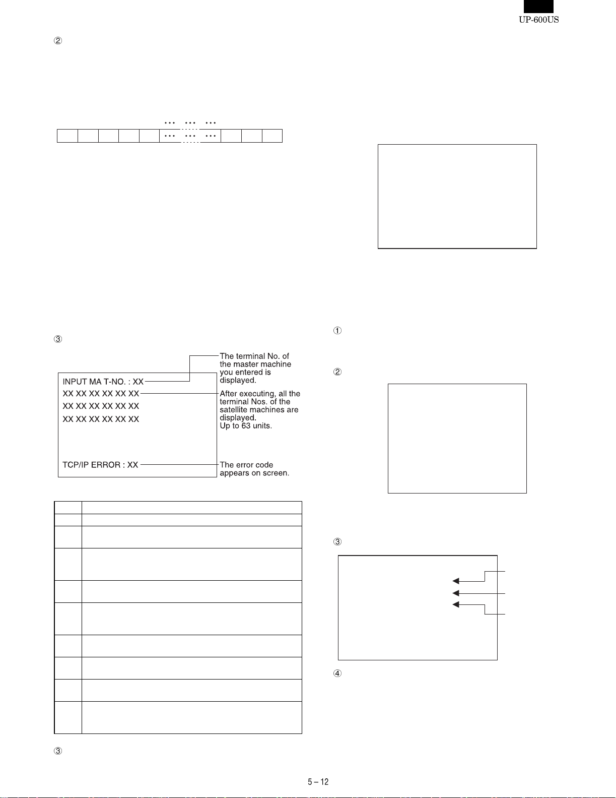
Setting
i. Setting satellite machines.
On the menu screen, select DATA Trans. (SA). The screen is
shown below.
DATA Trans.(SA)
INPUT SA T-NO.
Enter the terminal No. of the machine you are going to test (a
2-digit number from 1 - 32) + Enter. The screen looks like this:
DATA Trans.(SA)
INPUT SA T-NO. : XX
DATA SEQ.NO. : 0000
Enter a number
within the range
from 1 64.
The terminal No. you
entered is displayed.
i. Setting the master machine.
On the menu screen, select DATA Trans. (MA). The screen
looks like this:
DATA Trans.(MA)
INPUT MA T-NO. :
Enter a number
within a range
from 1~64.
Enter the terminal No. of the machine you want to test (a
2-digit number from 1 - 64)+ Enter. The screen looks like this:
DATA Trans.(MA)
INPUT MA T-NO. : XX
INPUT SA T-NO. :
The terminal No. you
entered is displayed.
Enter the terminal No. (a 2-digit number from 1 -64) of the
satellite machines which are connected to the test machine +
Enter. The screen looks like this:
The terminal No. of
DATA Trans.(MA)
INPUT MA T-NO. : XX
INPUT SA T-NO. : XX( or XXXX)
the master machine
you entered is
displayed.
The terminal No. of
the satellite machine
you entered is
displayed.
When performing the test with multiple satellite machines, type their
terminal numbers (2-digit numbers within the range from 1~64) and
press Enter. In addition, you specify the satellite machines using the
area specification function without typing terminal numbers. This is
achieved by typing the first terminal number (2 digits) and the last
terminal number (2 digits) of the satellite machines and then press
Enter. For example, if you want to specify the terminal numbers of
satellite machines from 5 to 15, type "0515" for T-No. and press Enter.
When executing, press the Enter key without typing the terminal
numbers.
The display appears like this:
Note that the terminal numbers of the master machine and satellite machines should not be the same. When the terminal numbers
are to be specified using the area specification function, any terminal number that is used for the master machine will be excluded
from the specification of satellite machine terminal numbers.
INPUT MA T-NO. : XX
The terminal No. of
the master machine
you entered is
displayed.
DATA SEQ.NO. : 0000
With the above setting, data transfer is performed bet ween the
master machine and the satellite machines.
Page 29
Checking
i. The master machine sends data of the following form at con-
sisting of 2-byte sequence No. and 254-byte AAH data to the
satellite machine. The master machine displays the sequence
Nos.
Test data format (1 packet: 256 bytes)
12345 254255256byte
XX XX AA AA AA AA AA AA
7) MCR & DRAWER Diagnostics
The program checks the MCR and drawer.
The following menu appears on screen.
The cursor shown in reverse video can be moved using the up/down
arrow keys. Move the cursor to the m enu item you want to execute
and select by pressing the ENTER key to execute the corresponding
program. Press the CANCEL key to return the screen to this submenu.
XXXX : Sequence No. 2 bytes (4-digit binary coded decimal
number)
AA : Transfer (AAH) ~ 254 bytes
ii. The satellite machine returns the data it has received, to the
master machine as it is. The satellite machine displays the
sequence No. on the screen.
iii. The master machine receives the data and then checks the
sequence Nos. and 254-byte AAH data. If an error occurs, the
master machine displays an error code and ends the test. If
there are multiple satellite machines, steps i and ii are repeated.
The master machine advances the sequence No. when data is
transferred successfully between it and the satellite machines.
Steps i - iii are repeated.
Error display
The following error codes are used (same as for TCP/IP HANDLER)
01 Command error (excluding the time when data is sent)
02 No data received
03 Received data size present
Received data left
04 Receiving station not ready for receiving (when sending)
"NRDY" is returned because the receiving station is not
ready for receiving.
05 Receiving buffer full(when sending)
The receiving side’s controller receive buffer is full.
06 Resend error(When sending)
The number of retries exceeds the setting (5 times) when
no response is obtained.
07 Collision error (When sending)
If a collision occurs
08 Line busy time out
Data cannot be sent due to multiple stations communicating
09 Receiving data size over (when receiving)
Insufficient size of receiving buffer.
0A Hardware error
Interface error (No SRN interface or defective SRN
controller)
MCR&DRAWER Check
MCR Check
DRAWER 1 Check
DRAWER 2 Check
7)-1. Magnetic Card Reader Check
The program performs the read test of an optional UP-E13MR.
The test program reads a magnet card using the ISO7811/1-5 stand-
ard and prints data on the journal.
Press the CANCEL key to return the screen to the submenu.
Checking
The program reads tracks 1 - 3 of a magnet card using the
ISO7811/1‘5 standard and prints the data using ASCII codes.
JOURNAL print
MCR Check
TRACK1:
XXXXXXXXXXXXXXXXXXXXXXXXXXX
XXXXXXXXXXXXXXXXXXXXXXXXXXX
XXXXXXXXXXXXXXX
TRACK2:
XXXXXXXXXXXXXXXXXXXXXXXXXXX
TRACK3:
XXXXXXXXXXXXXXXXXXXXXXXXXXX
Data read by the MCR is printed in the areas XXXXX. If an error
occurs, the following error codes are displayed. Until the program
is terminated, the error code is repeated, standing by for reading.
Display
MCR Check
TRACK1 : BUFFER EMPTY
TRACK2 : MCR ERROR
TRACK3 : PASS
How to exit the program.
Press the CANCEL key to exit the program.
Receive data is
empty
Data error after
detecting card.
Data has been read
successfully.
How to exit the program
Press the CANCEL key to exit the program.
Page 30
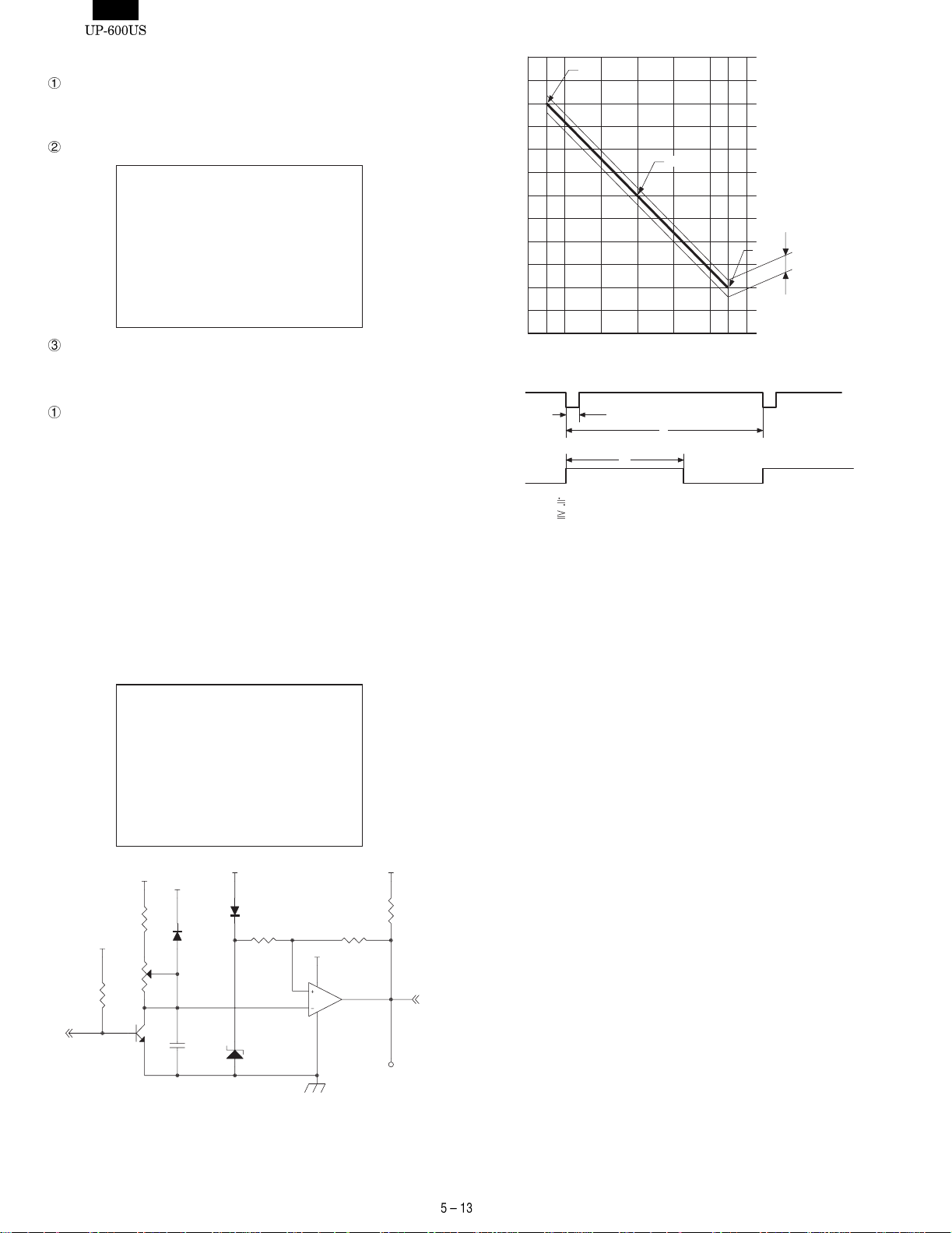
7)-2. Drawer 1 Check
Checking
The program turns on the drawer 1 solenoid, senses the value of the
drawer open sensor every 100 ms, and displays the operating status.
Display
DRAWER 1 Check
Open Sensor : OPEN (or CLOSE)
420
410
400
390
380
370
360
350
Transmission width (µs)
340
330
320
410
370
330
±3µs
(Allowance)
How to exit the program
Press the CANCEL key to exit the program.
7)-3. Drawer 2 Check
Checking
The program turns on the drawer 2 solenoid, senses the value of the
drawer to open the sensor every 100ms, and displays the operating
status. The procedure for displaying the menu and exiting the program are the same as for the drawer 1 check.
8) Dot Pulse Adjustment:
R/J printer dot pulse width adjustment
The dot pulse width adjust circuit is provided to control the width of
the current applied to the dot head of the printer, according to a
supply voltage fluctuation.
When the circuit is changed by repair work, the dot pul se width needs
to be adjusted using the 200k pot VR2.
Display
Dot pulse adjustment
2221.6 23 24 25 26 26.4
Drive voltage (V)
TRG
PE
PwPt4µsec
Pd is adjusted to 373±3µsec. when Vp is +24.0V.
Pw
Pd
1000µsec
Pt
D1
1SS355
C59
10000pF
+24V
D2
E102
ZD5
UDZ4.3B
R135
2K
TRG
R263
+24V
VCC
R81
130K"F"
VCC
VR2
200K
10K
Q5
KRC106S
How to exit the program.
Press the CANCEL key to exit the program.
VCC
R137
R136
62K
+24V
8
5
7
6
IC10B
4
BA10393F
3.3K
PE
TP
Page 31

CHAPTER 6. CIRCUIT DESCRIPTION
1. HARDWARE BLOCK DIAGRAM
DRAWER x 2
RS232 CH8
RS232 CH1
UP-P16DP
(POLE-DISP)
Controller
CKDC9
CPU
H8/510
SYSTEM
G/A
(MPCA9)
FLASH
ROM
Max.2MB
S-RAM(STD)
Max.512KB
S-RAM(STD)
Max.4MB
UP-S02MB:
2MB
UP-S04MB:
4MB
PRINTER
(DP-750)
MCR UNIT
UP-E13MR
LCD UNIT
LCD
Controller
M66271
KEY/SW/POP
Controller
CKDC9
Optional
CARD
ER-A5RS
Ethernet
Controller
(TCP/IP stack)
RS232 x 2
10base-T
Page 32

Symbol/PartsCod)
- - - - - - - - - - - - - - - - - - - - - - - - - - - - - - - - - - - - - - - - - - - - - - - - - - - - - - -
2. DESCRIPTION OF MAIN LSI’s
1) CPU (HD6415108FX)
1)-1. Pin descriptio n
MD2
MD1
MD0
VCC
STBY
RFSH
LWR
HWRRDAS
E
X
VSS
XTAL
VSS
EXTAL
TXD2
TXD1
RXD2
RXD1
IRQ1
SCK2/IRQ3
SCK1/IRQ2
IRQ0
VCC
P73
AVCC
P72
RES
NMI
VSS
P10
P11
P12
P13
P14
P15
P16
P17
D8
D9
D10
D11
D12
D13
D14
D15
VSS
A0
A1
A2
A3
A4
A5
A6
A7
112
111
110
109
108
107
106
105
104
103
1
2
3
4
5
6
7
8
9
10
11
12
13
14
15
16
17
18
19
20
21
22
23
24
25
26
27
28
293031323334353637383940414243444546474849505152535455
102
999897969594939291908988878685
101
100
56
84
83
82
81
80
78
78
77
76
75
74
73
72
71
70
69
68
67
66
65
64
63
62
61
60
59
58
57
P71
P70
AVSS
VSS
P67
P66
P65
P64
P63
P62
P61
P60
P57
P56
P55
P54
P53
P52
P51
P50
VSS
P47
P46
P45
P44
P43
P42
P41
A8
A9
A10
A11
A12
A13
A14
A15
VSS
A16
A17
A18
A19
A20
A21
A22
A23
VSS
P30/WAIT
P31/BACK
P33
P34
P32/BREQ
P35
P36
P37
VCC
P40
Page 33

1)-2. Block diagram
D9
D15
D14
D13
D12
D11
Data bus Port 1
D10
D8
P17
P16
P15
P14
P13
P12
P11
P10
Port 2
P27/A23
P26/A22
P25/A21
P24/A20
P23/A19
P22/A18
P21/A17
P20/A16
EXTAL
XTAL
X
E
MD2
MD1
MD0
RES
STBY
NMI
AS
RD
HWR
LWR
RFSH
VCC
VCC
VCC
VSS
VSS
VSS
VSS
VSS
VSS
VSS
VSS
AVCC
AVSS
Clock
oscillator
Refresh controller
Wait state
controller
A/D convertor
Watch
dog timer
H8/500 CPU DTC
Interruption controller
16bit free running
timer x 2ch
8bit timer
Serial
communication
interface x 2ch
Data bus (Lower)
Data bus (Upper)
Address bus
A15
A14
A13
A12
A11
A10
A9
A8
A7
A6
Address bus
A5
A4
A3
A2
A1
A0
P37
P36
P35
P34
Port 3Port 4
P33
BREQ
BACK
WAIT
P47
P46
P45
P44
P43
P42
P41/TMCI
P40
Port 5Port 6Port 7Port 8
TXD2
RXD2
TXD1
RXD1
SCK2/IRQ3
IRQ1
IRQ0
SCK1/IRQ2
P73
P72
P71
P70
P67
P66
P65
P64
P63
P62
P61
P60
P57
P56
P55
P54
P53
P52
P51
P50
Page 34

1)-3. Pin description
Pin
Symbol
No.
1 /RES /RESET In Reset signal
2 NMI NMI In
3 VSS GND In GND
4 D0 D0 I/O Data bus
5 D1 D1 I/O Data bus
6 D2 D2 I/O Data bus
7 D3 D3 I/O Data bus
8 D4 D4 I/O Data bus
9 D5 D5 I/O Data bus
10 D6 D6 I/O Data bus
11 D7 D7 I/O Data bus
12 D8 D8 I/O Data bus
13 D9 D9 I/O Data bus
14 D10 D10 I/O Data bus
15 D11 D11 I/O Data bus
16 D12 D12 I/O Data bus
17 D13 D13 I/O Data bus
18 D14 D14 I/O Data bus
19 D15 D15 I/O Data bus
20 VSS GND In GND
21 A0 A0 Out Address bus
22 A1 A1 Out Address bus
23 A2 A2 Out Address bus
24 A3 A3 Out Address bus
25 A4 A4 Out Address bus
26 A5 A5 Out Address bus
27 A6 A6 Out Address bus
28 A7 A7 Out Address bus
29 A8 A8 Out Address bus
30 A9 A9 Out Address bus
31 A10 A10 Out Address bus
32 A11 A11 Out Address bus
33 A12 A12 Out Address bus
34 A13 A13 Out Address bus
35 A14 A14 Out Address bus
36 A15 A15 Out Address bus
37 VSS GND In GND
38 A16 A16 Out Address bus
39 A17 A17 Out Address bus
40 A18 A18 Out Address bus
41 A19 A19 Out Address bus
42 A20 A20 Out Address bus
43 A21 A21 Out Address bus
44 A22 A22 Out Address bus
45 A23 A23 Out Address bus
46 VSS GND In GND
47 P30 /WAIT In Wait signal
48 P31 /BACK Out
49 P32 /BREQ In Bus control request signal
50 P33 DOPS In Drawer open signal
51 P34 /DR0 Out Option drawer open signal
52 P35 /DR1 Out Option drawer open signal
53 P36 NC NC NC
54 P37 NC NC NC
55 VCC VCC In +5V
56 P40 VCC In +5V
57 P41 GND In GND
58 P42 GND In GND
Signal
name
In/
Out
Non-maskable interrupt input
for SSP interrupt input.
Bus control request
acknowledge signal
Function
Pin
Symbol
No.
59 P43 GND In GND
60 P44 MCRINT In MCR interrupt signal
61 P45 GND In GND
62 P46 /SHEN In
63 P47 GND In GND
64 VSS GND In GND
65 P50 – Out /DTR2 : Data Terminal Ready2
66 P51 – In /DSR2 : Data Set Ready2
67 P52 – In /CTS2 : Clear To Send2
68 P53 – In /DCD2 : Carriar Detect2
69 P54 – In NC
70 P55 NC Out /RTS2:Request To Send2
71 P56 – In /CI2:Calling Indicator2
72 P57 /STOP Out System reset output signal
73 P60 /IPLON0 In From IPL SW
74 P61 /IPLON1 In From IPL SW
75 P62 GND In GND
76 P63 NORDY In Flash Memory ready ("H" active)
77 P64 FVPON Out
78 P65 BANK Out For IPL ROM
79 P66 GND In GND
80 P67 GND In GND
81 VSS GND In GND
82 AVSS GND In GND
83 P70 GND In GND
84 P71 GND In GND
85 P72 GND In GND
86 P73 GND In GND
87 AVCC VCC In +5V
88 VCC VCC In +5V
89 /IRQ0 /IRQ0 In Interrupt signal 0
90 /IRQ1 /IRQ1 In Interrupt signal 1
91 /IRQ2 UASCK In
92 /IRQ3 SCKI Out
93 RXD1 /RCVDT2 In RXD signal for RS232
94 TXD1 TXD2 Out TXD signal for RS232
95 RXD2 RXDI In CKDC interface shift input data
96 TXD2 TXDI Out
97 VSS GND In GND
98 EXTAL EXTAL In
99 XTAL XTAL In
100 VSS GND In GND
101 X # Out System clock
102 E NC NC NC
103 /AS /AS Out Address strobe
104 RD /RD Out Read signal
105 /HWR /HWR Out Write signal (HIGH)
106 /LWR /LWR Out Write signal (LOW)
107 /RFSH /RFSH Out Refresh cycle signal
108 VCC VCC In +5V
109 MD0 IPLON0 In From IPL SW
110 MD1 IPLON0 In From IPL SW
111 MD2 /IPLON0 In From IPL SW
112 /STBY VCC In +5V
Signal
name
In/
Out
CKDC interface shift enable
signal
Flash Memory write protect ("L"
active)
Synchronizing shift clock signal
for USART
CKDC interface synchronizing
shift clock
CKDC interface shift output
data
Crystal oscillator connection
19.6MHz
Crystal oscillator connection
19.6MHz
Function
Page 35

2) G.A.(MPCA9)
2)-1. Pin configuration
VDD
GND
GND
ST3# DOT3
ST2# DOT2
ST1# DOT1
NC
TTHR
RTS3#
DTR3#
RXRDY3
TRXRDY3
TXD3
TXRDY3
TRXC3
RXD3
BUSY3#
EXINT3#
EXINT2#
EXINT1#
EXINT0#
EXWAIT#
DSF2#
VWAIT#
DSF1#
DSCX#
GND
VDD
OPTCS#
IPLON
RXC1
RXD1
DSR1#
RXC2
RXD2
DSR2#
RXC4
RXD4
DSR4#
STH2
SCK2#
HTS2
INT4#
RTS5#
DTR5#
TXD5
RXD5
CTS5#
DSR5#
CI5#
CD5#
GND
GND
156
155
154
153
152
151
150
149
148
147
146
145
144
143
142
141
140
139
138
137
136
135
134
133
132
131
130
129
128
127
126
125
124
123
122
121
120
119
118
117
116
115
114
113
112
111
110
109
108
107
106
105
157
104
ST4# DOT4
ST5# DOT5
GND
ST6# DOT6
LATCH# DOT7
SO DOT8
GND
CLOCK DOT9SIDTCS
WO LCDWT
DTST#
INHDEC
CSEN#
TTST2#
TTST1#
TIRQ#
INH#
RPE
JPE
PHUP PE
PCRES
PFP
VHCOM
GND
VDD
RVPON TRG#
JVPON TRG
CTBO PCUT#
CTAO FCUT#
RDS PRST#
RCS PTMG#
RBS RJMTD
RAS RJMTS
JDS STAMP#
JCS VF#
JBS RF#
JAS JF#
PTRM RJTMG
PTJM TRGI
POPI RJRST
BA15
BA14
158
159
160
161
162
163
164
165
166
167
168
169
170
171
172
173
174
175
176
177
178
179
180
181
182
183
184
185
186
187
188
189
190
191
192
193
194
195
196
197
198
199
200
103
102
101
10099989796959493929190898887868584838281807978777675747372717069686766656463626160595857565554
GND
201
BA13
BA12
BA11
BA10
BA9
BA8
VDD
202
203
204
205
206
207
208
1
2
3
4
5
6
7
8
9
10
11
12
13
14
15
16
17
18
19
20
21
22
23
24
25
26
27
28
29
30
31
32
33
34
35
36
37
38
39
40
41
42
43
44
45
46
47
48
49
50
51
52
53
GND
GND
BA7
BA6
BA5
BA4
BA3
BA2
BA1
GND
BA0
BWR#
BRD#
BRAS
BRAS#
BD7
BD6
BD5
GND
BD4
BD3
GND
BD2
BD1
BD0
GND
VDD
INT3#
INT2#
INT1#
INT0#
HTS1
SCK1#
STH1
IPLON#
RESET#
UTST#
USEL0
USEL1
USEL2
MCRINT
WAIT#
FROS1#
RASPN1
RASPN2
EPROM1#
DSEX#
RXDH
TXDH
SCKH
GND
GND
VDD
A23
A22
A21
A20
A19
A18
A17
A16
A15
A14
A13
A12
A11
A10
A9A8A7A6A5A4A3A2A1
A0
D7D6D5
D4
D3
GND
VDD
GND
GND
D2D1D0
GND
SSPRQ#
AS#
RD#
MD0
WR#
IRQ1#
IRQ0#
MD1
PHAI
GND
UASCK
VDD
OSI1
OSO1
Page 36

2)-2. Block diagram
A23~A0
D7~D0
/AS,/RD,/WR
PHAI,/RESET
USEL2~USEL0, UTST#
MPCA9
INT4#~INT0#
MCRINT
WAIT#
FROS1#,EPROM1#
RASPN1,2
DSEX#
RXDH,TXDH,SCKH
OSO1,OSI1
USACK
MD1,MD2
IRQ0#
SSPRQ#
HTS2,SCK2,STH2
RXD4,RXC4,DSR4#
RXD2,RXC2,DSR2#
RXD1,RXC1,DSR1#
IPLON
OPTCS#
VMEMC#,VIOC#
DSF2#
VWAIT#,EXWAIT#
EXINT0#,EXINT1#
EXINT2#,EXINT3#
BUSY3#,RXD3,TXD3
TRXC3,TXRDY3
TRXRDY3,RXRDY3
DTR3#,RTS3#
VRESC
DTCS,DTST#
LCDWT
MPCA
OPC
IRQ1#
TXD5,RXD5
DTR5#,RTS5#
DSR5#,CTS5#
CD5#,CI5#
DBTST
DOT1,DOT2
DOT3,DOT4
DOT5,DOT6
DOT7
DOTEN,RJMTR
PCUT#,FCUT#
TRG#,TRG
PRST#,PTMG#
RJMTD,RJMTS
STAMP#
VF#,RF#,JF#
RJTMG,RJRST
TRGI
Page 37

2)-3. Pin description
Pin
Name IN/OUT Description
No.
1 GND - GND
2 GND - GND
3 BA7 O Address bus 7 for PB-RAM (NU)
4 BA6 O Address bus 6 for PB-RAM (NU)
5 BA5 O Address bus 5 for PB-RAM (NU)
6 BA4 O Address bus 4 for PB-RAM (NU)
7 BA3 O Address bus 3 for PB-RAM (NU)
8 BA2 O Address bus 2 for PB-RAM (NU)
9 BA1 O Address bus 1 for PB-RAM (NU)
10 GND - GND
11 BA0 O Address bus 0 for PB-RAM (NU)
12 BWR# O PB-RAM write strobe signal (NU)
13 BRD# O PB-RAM read strobe signal (NU)
14 BRAS O PB-RAM chip select : Active High (NU)
15 BRAS# O PB-RAM chip select : Active Lo w (NU)
16 BD7 I/O Data Bus 7 for PB-RAM (NU)
17 BD6 I/O Data Bus 6 for PB-RAM(NU)
18 BD5 I/O Data Bus 5 for PB-RAM (NU)
19 GND - GND
20 BD4 I/O Data Bus 4 for PB-RAM (NU)
21 BD3 I/O Data Bus 3 for PB-RAM (NU)
22 GND - GND
23 BD2 I/O Data Bus 2 for PB-RAM (NU)
24 BD1 I/O Data Bus 1 for PB-RAM (NU)
25 BD0 I/O Data Bus 0 for PB-RAM (NU)
26 GND - GND
27 VDD - +3.3V
28 INT3# I Interrupt signal 3 (NU)
29 INT2# I Shift enable for CKDC9
30 INT1# I Keyboard request for CKDC9
31 INT0# I Power off signal input
32 HTS1 O 8 bit serial port output (for CKDC9)
33 SCK1# O Serial port shift clock output (for CKDC9)
34 STH1 I 8 bit serial port input (for CKDC9)
35 IPLON# I IPL switch 0 ON signal
36 RESET# I MPCA reset
37 UTST# I MPCA test pin (+3.3V)
38 USEL0 I MPCA test pin (GND)
39 USEL1 I MPCA test pin (GND)
40 USEL2 I MPCA test pin (GND)
41 MCRINT O MCR interrupt signal
42 WAIT# O Wait request signal
43 FROS1# O Flash ROM 1 chip select signal
44 RASPN1 O RAM 1 chip select signal
45 RASPN2 O RAM 2 chip select signal
46 EPROM1# O EP-ROM 1 chip select signal
47 DSEX# O EP-ROM 2 chip select signal
48 RXDH O 8 bit serial port output to CPU
49 TXDH I 8 bit serial port input from CPU
50 SCKH I Serial port shift clock input from CPU
51 GND - GND
52 GND - GND
53 VDD - +3.3V
54 OSO1 O System clock (7.37MHz)
Pin
Name IN/OUT Description
No.
55 OSI1 I System clock (7.37MHz)
56 GND - GND
57 UASCK O USAT clock to CPU
58 MD1 I MPCA test pin (GND)
59 MD0 I MPCA test pin (GND)
60 PHAI I System clock (9.83MHz)
61 AS# I Address strobe
62 RD# I Read Strobe
63 WR# I Write Strobe
64 IRQ0# O Interrupt request 0 to CPU
65 IRQ1# O Interrupt request 1 to CPU
66 SSPRQ# O SSP interrupt request to CPU
67 GND - GND
68 D0 I/O Data Bus 0
69 D1 I/O Data Bus 1
70 D2 I/O Data Bus 2
71 GND - GND
72 D3 I/O Data Bus 3
73 D4 I/O Data Bus 4
74 GND - GND
75 D5 I/O Data Bus 5
76 D6 I/O Data Bus 6
77 D7 I/O Data Bus 7
78 VDD - +3.3V
79 GND - GND
80 A0 I Address bus 0
81 A1 I Address bus 1
82 A2 I Address bus 2
83 A3 I Address bus 3
84 A4 I Address bus 4
85 A5 I Address bus 5
86 A6 I Address bus 6
87 A7 I Address bus 7
88 A8 I Address bus 8
89 A9 I Address bus 9
90 A10 I Address bus 10
91 A11 I Address bus 11
92 A12 I Address bus 12
93 A13 I Address bus 13
94 A14 I Address bus 14
95 A15 I Address bus 15
96 A16 I Address bus 16
97 A17 I Address bus 17
98 A18 I Address bus 18
99 A19 I Address bus 19
100 A20 I Address bus 20
101 A21 I Address bus 21
102 A22 I Address bus 22
103 A23 I Address bus 23
104 VDD - +3.3V
105 GND - GND
106 GND - GND
107 CD5# I RS-232 ch1 CD signal
108 CI5# I RS-232 ch1 CI signal
Page 38

Pin
Name IN/OUT Description
No.
109 DSR5# I RS-232 ch1 DSR signal
110 CTS5# I RS-232 ch1 CTS signal
111 RXD5 I RS-232 ch1 RXD signal
112 TXD5 O RS-232 ch1 TXD signal
113 DTR5# O RS-232 ch1 DTR signal
114 RTS5# O RS-232 ch1 RTS signal
115 INT4# I Shift enable for option display
116 HTS2 O 8 bit serial port output (for option display)
117 SCK2# O
Serial port shift clock output
(for option display)
118 STH2 I 8 bit serial port input (for option display)
119 DSR4# I MCR track 3 CLS signal
120 RXD4 I MCR track 3 RDD signal
121 RXC4 I MCR track 3 RCP signal
122 DSR2# I MCR track 2 CLS signal
123 RXD2 I MCR track 2 RDD signal
124 RXC2 I MCR track 2 RCP signal
125 DSR1# I MCR track 1 CLS signal
126 RXD1 I MCR track 1 RDD signal
127 RXC1 I MCR track 1 RCP signal
128 IPLON O IPL switch 0 ON signal to CPU
129 OPTCS# O
Chip select base signal for expansion
option
130 VDD - +3.3V
131 GND - GND
132 VMEMC# O VRAM chip select signal
133 VIOC# O LCDC chip select signal
134 VWAIT# I LCDC wait signal
135 DSF2# O DPRAM chip select signal
136 EXWAIT# I External wait signal
137 EXINT0# I External interrupt signal 0
138 EXINT1# I External interrupt signal 1
139 EXINT2# I External interrupt signal 2
140 EXINT3# I External interrupt signal 3
141 BUSY3# I Fiscal memory BUZY signal (NU)
142 RXD3 I Fiscal memory RXD signal (NU)
143 TRXC3 I Fiscal memory CLOCK signal (NU)
144 TXD3 O Fiscal memory TXD signal (NU)
145 TXRDY3 O NU
146 TRXRDY3 O NU
147 RXRDY3 O Fiscal memory READY signal (NU)
148 DTR3# O Fiscal memory DTR signal (NU)
149 RTS3# O Fiscal memory RTS signal (NU)
150 DBTST I MPCA test pin (GND)
151 VRESC O NU
152 DOT1 O Printer dot signal 1
153 DOT2 O Printer dot signal 2
154 DOT3 O Printer dot signal 3
155 GND - GND
156 GND - GND
157 VDD - +3.3V
158 DOT4 O Printer dot signal 4
159 DOT5 O Printer dot signal 5
160 GND - GND
161 DOT6 O Printer dot signal 6
162 DOT7 O Printer dot signal 7
Pin
Name IN/OUT Description
No.
163 DOT8 O Printer dot signal 8 (NU)
164 GND - GND
165 DOT9 O Printer dot signal 9 (NU)
166 SI I Thermal head serial return data (NU)
167 DTCS O Printer control select signal (+3.3V)
168 LCDWT I Wait request signal to CPU (+3.3V)
169 DTST# I MPCA test pin (+3.3V)
170 INHDEC I CSEN# enable signal (GND)
171 CSEN# I TPRC chip select (GND)
172 TTST2# I MPCA test pin (+3.3V)
173 TTST1# I MPCA test pin (+3.3V)
174 TIRQ# O TPRC interrupt request (NU)
175 INH# I Thermal head drive inhibit (GND)
176 RPE I Receipt paper end signal (GND)
177 DOTEN O Dot driver enable signal
178 RJMTR I Printer motor lock detection signal (GND)
179 PCRES I Auto cutter unit reset signal (NU)
180 PFP I Auto cutter unit FP signal (NU)
181 VHCOM O Head drive common power control (NU)
182 GND - GND
183 VDD - +3.3V
184 PCUT# O Printer partial cut signal (NU)
185 FCUT# O Printer auto cut signal (NU)
186 TRG# O Dot head trigger signal
187 TRG O Dot head trigger signal (NU)
188 PRST# O Printer reset signal
189 PTMG# O Printer timing signal
190 RJMTD I Printer reset signal
191 RJMTS I Printer timing signal
192 STAMP# O Printer stamp solenoid drive signal
193 VF# O Multi line validation paper feed
194 RF# O
195 JF# O
Receipt side paper feed solenoid drive
signal
Journal side paper feed solenoid drive
signal
196 R JTG I Printer timing signal
197 TRGI I Journal motor connector sense signal
198 RJRST I GND
199 BA15 O Address bus 15 for PB-RAM (NU)
200 BA14 O Address bus 14 for PB-RAM (NU)
201 GND - GND
202 BA13 O Address bus 13 for PB-RAM (NU)
203 BA12 O Address bus 12 for PB-RAM (NU)
204 BA11 O Address bus 11 for PB-RAM (NU)
205 BA10 O Address bus 10 for PB-RAM (NU)
206 BA9 O Address bus 9 for PB-RAM (NU)
207 BA8 O Address bus 8 for PB-RAM (NU)
208 VDD - +3.3V
Page 39

3) CKDC9 (HD404728B02FS)
3)-1. General description
The CKDC9 is a 4-bit microcomputer developed for the UP-600 and
provides functions to control the real-time clock, keys, and displays.
The basic functions of the CKDC7 are shown below.
Keys: The CKDC9 is capable of controlling a maximum of 256
momentary keys. (Sharp 2-key rollover control)
Simultaneous scanning of key and switch
(When a key is scanned, the state of a mode and clerk
switch is also buffered. The host can scan the state of
switch together with the key entry data at the same time
the key is scanned.)
Switches: Mode switch with 14 positions maximum
8-bit clerk (cashier) switch
2-bit feed switch
1-bit receipt on/off switch
1-bit option switch
4-bit general-purpose switch (1-bit is used for keyboard
select)
Displays: 16-column dot display
12-column 7-segment display (column digit selectable)
All column blink controlled for the dot and 7-segment display decimal point and indicators
Programmable patterns for 7-segment display:
Four patterns
Internal driver for 7-segment display
Buzzer: Single tone control
Clock: Year, month, day of month, day of week, hour, minute
Alarm: Hour, minute
Interrupt request (event control):
Detection of key input, switch position change, alarm is-
sue, and counter overflow
3)-2. Pin description
Pin
Symbol
No.
1 SB SB Out Segment B
2 SC SC Out Segment C
3 SD SD Out Segment D
4 SE SE Out Segment E
5 SF SF Out Segment F
6 SG SG Out Segment G
7 P4 AP Out
8P0 NC—NC
9P1 NC—NC
10 P2 DP Out Decimal point
11 P3 ID Out Indicator
12
MODR VCC — +5V
CFSR CFSR In
13
14 KEX0 NC Out NC
15 KEX1 NC Out NC
16 RQ GND — GND
17 SKR0 VCC — +5V
18 ST0 ST0 Out Key strobe signal
19 ST1 ST1 Out Key strobe signal
20 ST2 ST2 Out Key strobe signal
21 ST3 ST3 Out Key strobe signal
22
POFF POFF In Power off signal
23
STOP STOP In STOP signal
24
DDIG VCC — +5V
Signal
name
In/
Out
Function
Clerk key, Feed key, Switch
return signal
Pin
Symbol
No.
25
DCS DCS —
26 VCC
27
SCK SCK In Clock signal
Signal
name
In/
Out
Dot display controller chip select
DCS
VCKDC — +5V
Function
28 HTS HTS In Key data from host
29 STH STH Out Key data to host
30 SDISP GND — GND
31 BUZZ BUZZ Out Buzzer
32
DSCK DSCK — Dot display controller SCK
33
SRES RESET Out Reset signal
34 DS0
35
SHEN SHEN Out Shift enable signal
36
IRQ KRQ Out Key request signal
37 KR0
38 KR1
39 KR2
40 KR3
DSO — Dot display controller SO
KR0 In Key return signal
KR1 In Key return signal
KR2 In Key return signal
KR3 In Key return signal
41 RESET CKDCR In CKDC reset signal
42 OSC2 OSC2 — Clock
43 OSC1 OSC1 — Clock
44 GND GND — GND
45 CL1 CL1 — Time clock
46 CL2 CL2 — Time clock
47 TEST VCKDC — +5V
48 G0 G1 Out Display digit signal
49 G1 G2 Out Display digit signal
50 G2 G3 Out Display digit signal
51 G3 G4 Out Display digit signal
52 G4 G5 Out Display digit signal
53 G5 G6 Out Display digit signal
54 G6 G7 Out Display digit signal
55 G7 G8 Out Display digit signal
56 G8 G9 Out Display digit signal
57 G9 G10 Out Display digit signal
58 G10 G11 Out Display digit signal
59 G11 NC Out NC
60 PO0 NC NC
61 PO1 NC NC
62 PO2 NC — NC
63 PO3 NC — NC
64 SA SA — Segment A
4) LCD CONTROLLER (M66271FB)
4)-1. Pin configration
BHE
D15
D14
D13
D12
D11
MPUCLK
OSC1
UD0
UD1
UD2
UD3
FLM
RESET
WAIT
MCS
LWR
HWR
IOCS
D10D9D8D7D6D5D4D3D2D1D0
1460595857565554535049484746454443776352423423
9
78
66
CP
67
LP
69
70
71
72
68
11
7
6
5
RD
4
3
2
127976747375323938373633518065140352413256441
N.C
N.C
N.C
N.C
N.C
N.C
N.C
N.C
N.C
N.C
OSC2
MPUSEL
VSS
VDD
VDD
VSS
VSS
VSS
VSS
VSS
VSS
VDD
VDD
VDD
VDD
VDD
8
31
A13
30
A12
29
A11
28
A10
27
A9
26
A8
22
A7
21
A6
20
A5
19
A4
18
A3
17
A2
16
A1
15
A0
62
M
61
LCDENB
10
VSS
VSS
VSS
VSS
VSS
Page 40

4)-2. Pin configration
Pin
No.
10 VSS GND
11 RESET# Reset input
12 MPUSEL 8/16-bit selective input to MPU
13 VSS GND
14 BHE# Bus high enable input
15 A0 MPU address bus 0
16 A1 MPU address bus 1
17 A2 MPU address bus 2
18 A3 MPU address bus 3
19 A4 MPU address bus 4
20 A5 MPU address bus 5
21 A6 MPU address bus 6
22 A7 MPU address bus 7
23 VDD +5V
24 VSS GND
25 VSS GND
26 A8 MPU address bus 8
27 A9 MPU address bus 9
28 A10 MPU address bus 10
29 A11 MPU address bus 11
30 A12 MPU address bus 12
31 A13 MPU address bus 13
32 N.C
33 N.C
34 VDD +5V
35 VSS GND
36 N.C
37 N.C
38 N.C
39 N.C
40 VSS GND
41 VSS GND
42 VDD +5V
43 D0 MPU data bus 0
44 D1 MPU data bus 1
45 D2 MPU data bus 2
46 D3 MPU data bus 3
47 D4 MPU data bus 4
48 D5 MPU data bus 5
49 D6 MPU data bus 6
50 D7 MPU data bus 7
51 VSS GND
52 VDD +5V
53 D8 MPU data bus 8
54 D9 MPU data bus 9
Name Description
1 VSS GND
2 IOCS# Chip select input for control register
3 HWR# High write strobe input
4 LWR# Low write strobe input
5 RD# Read strobe input
6 MCS# Chip select input for VRAM
7 WAIT# WAIT output to MPU
8 VDD +5V
9 MPUCLK MPU clock
Pin
No.
Name Description
55 D10 MPU data bus 10
56 D11 MPU data bus 11
57 D12 MPU data bus 12
58 D13 MPU data bus 13
59 D14 MPU data bus 14
60 D15 MPU data bus 15
61 LCDENB LCD (ON/OFF) control signal input
62 M LCD AC-conversion signal output
63 VDD +5V
64 VSS GND
65 VSS GND
66 CP Display data transfer clock
67 LP Display data clutch pulse
68 FLM FIRST LINE MARKER signal output
69 UD0 LCD display data bus 0
70 UD1 LCD display data bus 1
71 UD2 LCD display data bus 2
72 UD3 LCD display data bus 3
73 N.C
74 N.C
75 N.C
76 N.C
77 VDD +5V
78 OSC1 Oscillation input terminal
79 OSC2 Oscillation output terminal
80 VSS GND
Page 41

3. ADDRESS MAP
1) TOTAL MEMORY SPACE
The address map of the total memory space is shown below. As you
can see, the memory space is divided into the following 5 blocks:
0page area (including the I/O area)
• VRAM
• RAM
• ROM
• Extended I/O area
2) 0PAGE AREA
The 0page area consists of four spaces: the ROM mapped area,
internal and external I/O areas.
The ROM mapped area has been devised for the following purposes:
Simplifying the procedure for booting the IPL program
Achieving high-speed accessing, and accessing by abbreviated
instructions.
000000h
* The ROM area 200000h to
20FFFFh (ROS1 lower 64KB)
is mapped on the ROMmapping
area.
000000h
00FFFFh
200000h
600000h
800000h
C00000h
C20000h
D00000h
F00000h
FFFFFFh
0 page area
(64KB)
Flash
(4MB)
STD RAM (2MB)
EXTEND RAM
(4MB)
VRAM (128KB)
EP-ROM
(2MB)
Extended I/O area
(1MB)
* In the 0 page area, lower 64KB
or less of the flash area is
mapped.
By mapping the ROM area, the
reset start and other vectors
become addressable.
* The expanded I/O area means
the space for the I/O device
addressed in the area excluding
the 0 page one.
MPCA8 uses FFFF00h to
FFFFFFh for the addressed
register (BAR) of SSP.
The I/O register for VGAC is
included.
ROM mapping area
* The internal I/O area is used
for peripheral modules inside
the CPU; the external I/O area
is used for peripheral modules
outside the CPU.
For more information, refer to
the H8/510 hardware manual
and peripheral device
00FE80h
00FF80h
00FFFFh
Internal I/O area
External I/O area
specification.
I/O area
3) I/O AREAS
The addresses from 00FF80h to 00FFFFh are called the internal I/O
area.
The internal I/O area is a space where the control registers and
built-in ports inside the CPU are addressed.
The external I/O area is a space where the peripheral devices outside
the CPU or devices on an optional card are addressed.
00FE80h
Internal I/O area
00FF80h
00FFA0h
00FFB0h
00FFB4h
00FFB8h
00FFBCh
00FFC0h
00FFD0h
00FFE0h
00FFF0h
00FFFFh
MPCCS
Expanded MPC
(not used)
MCR1Z
MCR2Z
T/PZ
MCR3Z
OPCCS1
OPCCS2
CPCSZ (not used)
TPRC1
* MPCCS and expanded MPC
signals are base signals for
MPCA9 internal register
decode. There is no external
signal.
* MCR1Z and MCR2Z are chip
* MCR1Z, MCR2Z and MCR3Z
are chip select signals for the
magnet card reader.
(Use lower 2bytes.)
* T/PZ is the internal decode
signal for USART built in
MPCA9. Thereis no external
signal. (Use lower 2bytes.)
* OPCCS1 and OPCCS2
signals are decoded inside
the OPC (OPTION PERIP HERAL CONTROLLER)
using the option decode
signal OPTCS. There is no
external signal.
OPTCSZ
* CPCSZ is CPC select for
Centronics Interface.
TPRC1 is built in by
MPCA9.
Page 42

4) ROM SPACE
Fig.5 shows the ROM space. The UP-600 uses 2MB of NOR-type
flash memory instead of conventional ROM, so that the FROS1# from
the MPCA9 is input into the chip enable of the flash memory.
200000h
* Lower 64KB of the ROS1 is
mapped on the 0 page area.
ROS1
(MAX4MB)
* ROS1 is decoded by
MPCA9.
5FFFFF
5) VRAM & RAM SPACE
The VRAM is the display memory of the LCD.
1) BLOCK DIAGRAM
Here is the block diagram of the LCD and its allied components.
CPU
H8/510 SD0-7
RD#
HWR#
PHAI CLK
WAIT#
WAIT#
MPCA8
LCDWT
VIO# IOCS#
VMEM# MCS#
A0-13
RD#
LWR#
LCD (320 x 240)
M66271
UD0-3 LD0-3
LP LP
FLM FP
DCLK DCLK
MBIAS
LCDENB
8bitMPU connection setting
MPUSEL : "L"
BHE# : "H"
HWR# : "H"
VEE BACKLIGHT
POWER
600000h
800000h
A00000h
RASPN1
(2MB)
RASPN2
* All the decode signals in the
area in the figure are supported
by MPCA9.
* RAS1 signals from MPCA9
correspond to 2MB 600000h to
7FFFFFh.
* OPTION RAM board (2MB and
4MB) interfaces using RAS2
as the base signal.
(4MB)
C00000h
VRAM
(1MB)
* The actual VRAM is 128KB,
but it is accessed by every
128KB of bank according to
VGAC specification.
CFFFFFh
6) EXTENDED I/O AREA
The addresses from F00000h to FFFFFFh are called an extended I/O
area. The UP-600 uses the following addresses as the break address
register (BAR) for SSP.
• FFFF00h ∼ FFFFFFh
2) LCD PANEL
The LCD panel uses a dot-matrix liquid crystal module with monochromatic STN and CCFT backlight. The resolution is 320 x 240.
3) DISPLAY CONTROLLER
Matsushita VGAC (M66271) is used for the display controller.
VRAM is present on the address space of the CPU and it is possible
to write and read data from the CPU side through the lower 9600 byte
address of 128 KB size in addresses C00000H ~ C1FFFFH.
C00000H - C1FFFH:
4) LCD ON CONTROL
The LCD is turned on and off by controlling the bias power supply for
the LCD using the terminal LCDENB of the M66271.
LCDENB is in low level when resetting. When bit 0 of the mode
resistor of the M66271 by software is set to high level, the power is
supplied to the LCD, thus turning on the LCD.
5) BACK LIGHT CONTROL
The backlight ON/OFF is controlled by the same LCDENB used for
controlling the LCD ON mode.
6) LUMINANCE AND CONTRAST ADJUSTMENT
Luminance: Luminance is adjusted with an inverter which controls
•
the dimming function. (Fixed)
• Contrast: Contrast is adjusted by controlling the contrast adjust-
ment voltage (VO) of the LCD.
4. LCD DISPLAY
The UP-600 uses a 320 x 240 dot monochromatic LCD for the main
display and VGAC (M66271) for the display controller which is connected to H8/510 in the ISA bus connection mode.
5. CUSTOMER DISPLAY
The UP-600 can incorporate a UP-P16DP for the customer display.
6. SRAM (Standard)
The device is HYUNDAI 4MB SRAM (HY628400ALLT2-70 512K 8bit)
with an access time of 70ns.
Page 43

1) CPU INTERFACE
The figure below shows a typical pseudo SRAM interface in the UP-
600.
S RAM(Standard)
A0~A18
D0~D7
S RAM(Option)
74LV138
Y
/RD
/WR
/CE
A,B,C
A0~A18
A0~
A18
A19~
A21
/G
A0~A21
D8~D15
/RD
/RESET
MPCA9
/HWR
RASPN1
RASPN2
2) SRAM ADDRESS
Standard SRAM is decoded as follows by the RASPN1 signal.
780000h ∼ 7FFFFFh
The base signal is 2MB. It thus wraparounds with 600000H ∼
7FFFFFH 1.5MB.
7. NOR-type FLASH MEMORY
Here is the explanation for the interface of NOR-type flash memory.
The device is Sharp’s LH28F016SU flash memory which consists of
512 K words × 16 or 1 MB × 8, with 32 blocks of 64 KB.
1) CPU INTERFACE
The figure below shows a typical interface for the LH28F016SU of the
UP-600 system.
5V
H8/510
MPCA8
DATA
ADDRES
HWR-
RD-
PORT64
PORT63
FROS1-
FVPON
NORDY
RESET-
DQ0~DQ1
A0~A2
WE#
OE#
WP#
RY/BY#
RP#
CE0#
CE1#
LH28F
016SUT
BYTE#
VCC
VPP
3/5#
GND
8. SSP CONTROL
The UP-600 uses flash memory in the place of EPROM, so it is
possible to rewrite the contents of the flash memory in changing the
program. However, since the existing gate array MPCA8 is used, it is
also possible to use the conventional SSP.
1) OPERATION
Like the MPCA5 ~ 8, the MPCA9 adopts the break address register
comparison method for detecting addresses. The operation of this
method is briefly explained below.
The gate array always compares the break address register (BAR)
built in the gate array, with the address bus to monitor the address
bus.
If both agree, the gate array outputs the NMI signal to the CPU, which
in turn shifts from normal handling to exception handling.
In both the MPCA5 ~ 8 and the MPCA9, SSP is achieved by the
above operation.
The setting of the break address register (BAR) is directly written in
the addresses from FFFF00h to FFFFFFh.
9. INTERRUPT CONTROL
There are roughly two types of interrupts:
• Internal interrupts: Controlled inside the CPU
• External interrupts: Input into the CPU from outside
1) INTERNAL INTERRUPTS
Device interrupts built in the CPU are used for the f ollowing applications:
Event factor Application
SC11 Interrupt source as RS232 : CH8
SC12 Not used (SC1 is used for CKDC interface.)
FRT1 (ICI)
(OCRA)
(OCRB)
(OVF)
FRT2 (ICI) Standard SHEN event (for CKDC)
(OCRA) Simple IRC timer event
(OCRB) RS232 timer event
(OVF) System timer (53 ms)
TMR (CMA)
(CMB)
(OVF)
WDT (OVF) Drawer open timer
A/D Not used
NMI SSP request
2) EXTERNAL INTERRUPTS
The following types of external interrupts are available:
• NMI (SSP)
• IRQ0 (Standard I/O interrupt)
• IRQ1 (RS232 interrupt)
• IRQ2 (Not Used)
• IRQ3 (Used as SCK terminal)
INTMCR ∼ MCR interrupt (to FT11 terminal)
2) DEVICE CONTROL
After resetting, the device automatically enters the array read mode
and performs the same action as the usual ROM, thus requiring no
special consideration when reading data.
Data can be written at a high speed by using the page buffer.
Page 44

10. WAIT CONTROL
The weight control function built in the M PCA9 is used to provide an
interface with low-speed devices.
1) BLOCK DIAGRAM
The block diagram of the wait control function is shown.
WAIT
enable
For
RASP-
/AS
φ
CLK WAIT RESET Counter
START
/RESET for 1,2,3WAIT
D
/Q
/RESET
Selector
WAIT
Count
RASP
For
WAIT
enable
For
MISC
D
/Q
/RESET
Selector
WAIT
Count
For
MISC
WAIT
enable
For
VRAM
•
VGA
I/O
/RESET
for
1WAIT
D
/Q
WAIT
Count
For
RASPN
D
/Q
/RESET
Selector
WAIT
Count
For
RASPN
Terminal autoweight signal
/EXWAIT
/WAITZ
/VWAIT
/LCDWAIT
In the figure, the decoder, wait enabling regi ster, AND-OR sections
are the same as those in the MPCA6 or 7, but other components are
newly incorporated in the MPCA5.
EXWAITZ and WAITZ are external weight signals which are to be
ORed inside the MPCA9 and output to the WAITZ. The EXWAITZ is a
general-purpose wait request terminal, and WAITZ is the wait request
signal from the VGA controller.
11 . CKDC9
The UP-600 uses one CKDC9 for the CKDC PWB and one CKDC9
for the for POLE display (option) to carry out the following control
operations.
CKDC PWB:
• Clock (second data readable)
• Buzzer
• System reset
• Key/Clerk switch
Display PWB:
• Customer display tube
• Pole displ a y (UP-P16DP)
1) INTERFACE
The CKDC9 is connected through the MPCA8.
UP-P16DP
RESET
HTS
SCK
STH
MPCA8
TXDI
SCKI
RXDI
IRQ0
HTS2
SCK2
STH2
INT4
HTS1
SCK1
STH1
INT1
RESET
HTS
SCK
STH
SHEN
HTS
SCK
STH
KRQ
SHEN
SRES
STOP
CKDC9
H8/510
TXD2(P87)
SCK2(P83)
RXD2(P84)
STOP
(P57)
IRQ0
RES
FTI2
RESET
CKDC9
RESET
VFDC
reset from MAIN
Key
SW
Buzzer
VFD
Page 45

12. OPTION RAM INTERFACE
1) INTERFACE
The expanded RAM connector terminals are shown in the table below.
The 40-pin RAM is used for the connector.
Extension RAM connector terminals
Signal Name Pin No. Pin No. Signal Name
+5V 1 2 N.C.
HWR 3 4 N.C.
GND 5 6 A21
A20 7 8 A19
A18 9 10 A17
A16 11 12 A15
A14 13 14 A13
A12 15 16 A11
A10 17 18 A9
A8 19 20 A7
A6 21 22 A5
A4 23 24 A3
A2 25 26 A1
A0 27 28
D7 29 30 D6
D5 31 32 D4
D3 33 34 D2
D1 35 36 D0
RASPN2 37 38 VCKDC
GND 39 40 GND
RD
13. RESET SEQUENCE
The reset sequence block diagram is shown below. Note that the
RESET signal (system reset) and CKDCR signal (CKDC reset) are
different from each other.
VCC
SLIDE
SW
CKDCR
(CKDC reset)
1) POWER ON/OFF
The flow of signal processing at the time of the power supply turning
On/Off is as follows:
Table 19<Power OFF>
Power supply MPCA9 CPU CKDC9
POFF L
1
2
3
4
IRQ0 L
STOP L
RESET L
(System reset)
Table 20<Power ON>
Power supply MPCA9 CPU CKDC9
1
POFF H
2
3
STOP H
RESET H
(System reset)
The table below shows the timing chart.
Power supply On Power supply Off
+5V,+12V
PG GOOD
(POFF)
RESET
(System)
STOP
SHEN
SCK
8 PULSE
10ms MIN
14. DRAWER
The UP-600 can use up to 2 optional external drawers.
1) DRAWER SOLENOID DRIVE
P34 ∼ P37 inside the CPU are allocated for the port output of the
drawer solenoid drive.
CPU
IRQ0
STOP
RESET
(System reset)
CKDC9
MPCA9
POFF
INT0
POFF
POWER
SUPPLY
Built-in port Signal name Remarks
P34
P35
P36
P37
DR0 Drawer 1 (optional drawer)
DR1 Drawer 2 (optional drawer)
DR2 Reserved
DR3 Reserved
One port corresponds to one drawer. If a power failure is detected,
the drawer solenoid drive must be stopped as soon as possible.
The drawer solenoid drive time must be controlled in t he range of
40 ms to 50 ms by the timer.
2) DRAWER OPEN/CLOSE SENSE
The drawer open/close sense signal is input into the built-in port of
the CPU. The sense signal of an optional drawer sensor is also wired
ORed before inputting.
• P33=1: Any of the drawers is open.
Page 46

15. TCP/IP STACK
The LAN of the UP-600 uses as the protocol Ethernet, which supports
TCP/IP.
The interface with the TCP/IP board is achieved through 2 interrupt
signals and dual-port RAM.
The decode of dual-port RAM is located in the following space:
DP-RAM: F20000H - F2FFFFH (max. 64 KB)
The interruption from the TCP/IP is allocated as follows:
EXINTO: I N TSW (SLAVE WRITE interrupt) bit 6 of 00FF81H
EXINT1: INTSR (SLAVE READ interrupt) bit 0 of 00 FF8 0 H
<TCP/IP connector terminals>
Signal Name Pin No. Pin No. Signal Name
+5V 2 1 +5V
+5V 4 3 +5V
A14 6 5 A15
A12 8 7 A13
HWR 10 9 DPCS
A10 12 11 A11
A0 14 13
A2 16 15 A1
A4 18 17 A3
A6 20 19 A5
A8 22 21 A7
D7 24 23 A9
D5 26 25 D6
D3 28 27 D4
D1 30 29 D2
LRES 32 31 D0
INTSW 34 33 INTSR
-3635GND 38 37 GND
GND 40 39 GND
RD
1) CPU INTERFACE
The CPU interface for the USART (8251) and magnetic card reader
(MCM-21) in the UP-600 system is shown below.
x 2
8251
CLS1,
CLS2
RCVCLK1
/DSR2
RCVRDY1
RCVRDY2
RCVRDY3
RCVDT1
RCVCLK2
RCVDT2
RCVCLK3
RCVDT3
CPU
ICI
Integrated as MPCA8
in the UP-600 system.
INTMCR
INTMCR
MPCA7
RCVRDY1
RCVRDY2
SYNC
Signal description
RCP1 TRACK 1 CLOCK PULSE
RDD1 TRACK 1 DATA SIGNAL
RCP2 TRACK 2 CLOCK PULSE
RDD2 TRACK 2 DATA SIGNAL
RCP3 TRACK 3 CLOCK PULSE
RCD3 TRACK 3 DATA SIGNAL
CLS1 TRACK 1 CARD DETECTION SIGNAL
CLS2 TRACK 2 CARD DETECTION SIGNAL
CLS3 TRACK 3 CARD DETECTION SIGNAL
RCVRDY1 TRACK 1 DATA RECEIVING SIGNAL
RCVRDY2 TRACK 2 DATA RECEIVING SIGNAL
RCVRDY3 TRACK 3 DATA RECEIVING SIGNAL
INTMCR INTERRUPT SIGNAL OR-SYNTHESIZED from
RCVRDY and SYNC input
2 chip select signals for the 8251 are generated inside MPCA8.
RCP1
/DSR1
CLS2
/DSR3
RCP1
RDD1
RCP2
RDD2
CLS1
CLS2
RCP3
RDD3
CLS3
16. RS232
Two standard RS232 channels are compatible with the ER-A5RS.
However, while the ER-A5RS uses the
interruption of the RS232, the UP-600 cannot use the
instead of it. (The
IRQ2 terminal is used for IR as the SCK1 terminal.)
IRQ2 terminal of the CPU for
IRQ1 terminal
The standard RS232 is fixed to the logic channels 1 and 8. Use the
channels 2, 3, 4, 5, 6 and 7 for the ER-A5RS.
17. MCR
This paragraph describes the MCR option (UP-E13MR) control defined by the UP-600 hardware architecture.
3 channels of the serial port (interchangeable with 8251) built in the
MPCA9 are used. 3 tracks of data are read simultaneously. (UPE13MR)
2) MCR INTERFACE
The operating timing of the MCR interface signals is given below.
(1) Example of timing
CLS1/CLS2
CLS3
RCP1/RCP2
RCP3
RDD1/RDD2
RDD3
(2) Detailed timing (relation between DATA and CLOCK PULSE)
RCP1/RCP2
RCP3
RDD1/RDD2
RDD3
The "NULL" CODE is basically written prior to the opening code. The
opening code detection algorithm is considered because data may
become corrupt before and after the CARD detection signal due to a
worn magnet stripe.
"0" "1" "1"
Approx. 16µs
Min. 5µs
Page 47

CHAPTER 7. TCP/IP I/F PWB DESCRIPTION
1. GENERAL DESCRIPTION
This control board is an Ethernet board that supports the TCP/IP
protocol.
2. BLOCK DIAGRAM
10MHz
CN
/INTSR
/INTSW
Address
Data Bus
/DPCS,
/WR,/RD
Bus
LOGIC
Dual-Port
RAM
4k byte
/INTHR
/INTHW
/HWACK
/HRACK
/SWRQ
/SRRQ
/CS2
LD0~LD7
LA0~LA11
(SH-2)
Data Bus
CPU
/CS0
/CS1
/CS2
/CS3
LD0~LD7
LA0~LA18
Address Bus
LD0~LD7
LA0~LA18
/CS1
SRAM
128k byte
/CS0
FLASH
512k byte
3. CONFIGURATION
CPU :
[HitachiSH-2 Series SH7014 (20MHz)]
As external memory spaces, CS0 - CS3 and DRAM space are provided. This board assigns FLASH Memory to CS0, SRAM to CS1,
dual-port SRAM to CS2, and LAN controller to CS3.
LAN Controller : [RealtekRTL8019AS(20MHz)]
LAN controller is assigned to CS space.
Because of pseudo ISA connection, each register is assigned to ad-
dresses of H00C00300 and after.
ROM(FLASH Memory) :
[SharpLH28F004BVT(4Mbits)]
ROM (FLASH Memory) is assigned to CS0 space.
Data is written onto FLASH Memory from UV-EPROM by switching
the CSO space to UV-EPROM and the CS3 space to FALSH Memory.
MAC Address is written on FLASH Memory.
• Company code is assigned to "08001FH".
• The serial number and adjustm ent byte are stored in an area of 4
bytes from the address H’0007C000.
<The serial number is acquired according to Sharp’s in-house
specification(SS).>
<Access Time = 90ns>
/CS0
EP-ROM
(Writing in
to FLASH)
512k byte
RJ-45
/CS3
LAN Cnt.
(8bit-Bus)
LD0~LD7
LA0~LA19
LD0~LD7
LA0~LA18
When writing data into FLASH, switch /CS0to EP-ROM and /CS3
to FLASH Memory.
RAM : [S-RAM 1Mbits]<Access Time=70ns>
Assigned to CS1 space.
[IDT Dual-Port SRAM IDT7134]<Access Time=55ns>
Assigned to CS2 space.
The IDT7134 does not have any LOGICiBusy or Semaphorej, access
to the same address from both sides is inhibited.
Pulse Trans : [Pulse78Z034]
It is used for the 10Base-T standard and has a choke coil built in at
the output side.
Page 48

Symbol/PartsCod)
- - - - - - - - - - - - - - - - - - - - - - - - - - - - - - - - - - - - - - - - - - - - - - - - - - - - - - -
4. MAIN LSI DESCRIPTION
1) CPU (SH7014)
1)-1. SH7014 Overvi ew
The SH7014 CMOS single-chip microprocessors integrate a Hitachioriginal architecture, high-speed CPU with peripheral functions required for system configuration.
The CPU has a RISC-type instruction set. Most instructions can be
executed in one clock cycle, which greatly improves instruction execution speed. In addition, the 32-bit internal-bus architecture enhances data processing power. With this CPU, it has become possible to assemble low cost, high performance/high-functioning systems,
even for applications that were previously impossible with microprocessors, such as real-time control, which demands high speeds. In
particular, the SH7040 series has a 1-kbyte on-chip cache, which
allows an improvement in CPU performance during external memory
access.
In addition, this LSI includes on-chip peripheral f unctions necessary
for system configuration, such as large-capacity ROM (except the
SH7014, which is ROMless) and RAM, timers, a serial communication interface (SCI), an A/D converter, an interrupt controller, and I/O
ports. Memory or peripheral LSIs can be connected effi ciently with an
external memory access support function.
This greatly reduces system cost.
1)-1-1. SH7014 Features
CPU:
• Original Hitachi architecture
• 32-bit internal data bus
• General-register machine
– Sixteen 32-bit general registers
– Three 32-bit control registers
– Four 32-bit system registers
• RISC-type instruction set
– Instruction length: 16-bit fixed length for improved code effi-
ciency
– Load-store architecture (basic operations are executed be-
tween registers)
– Delayed branch instructions reduce pipeline disruption during
branch
– Instruction set based on C language
• Instruction executi on time: one instruction/cycle (35 ns/instruction
at 28.7-MHz operation)
• Address space: Architecture supports 4 Gbytes
• On-chip multiplier: multiplication operations (32 bits x 32 bits 64
bits) and multiplication/accumulation operations (32 bits x 32 bits +
64 bits
64 bits) executed in two to four cycles
• Five-stage pipeline
Cache Memory:
• 1-kbyte instruction cache
• Caching of instruction codes and PC relative read data
• 4-byte line length (1 longword: 2 instruction lengths)
• 256 entry cache tags
• Direct map method
• On-chip RAM, and on-chip I/O areas not objects of cache
• Used in common with on-chip RAM; 2 kbytes of on-chip RAM used
as address array/data array when cache is enabled
Interrupt Controller (INTC):
• Seven external interrupt pins (NMI, IRQ x 6)
• Twenty-eight internal interrupt sources
• Sixteen programmable priority levels
Bus State Controller (BSC):
• Supports external extended memory access
– 8-bit, or 16-bit external data bus
• Memory address space divided into five areas (four areas of
SRAM space, one area of DRAM space) with the following settable
features:
– Number of wait cycles
– Outputs chip-select signals for each area
– During DRAM space access:
• Outputs RAS and CAS signals for DRAM
• Can generate a RAS precharge time assurance Tp cycle
• DRAM burst access function
– Supports high-speed access mode for DRAM
• DRAM refresh function
– Programmable refresh interval
– Supports CAS-before-RAS refresh and self-refresh modes
• Wait cycles can be inserted using an external WAIT signal
• Address data multiplex I/O devices can be accessed
Note: No bus release
Direct Memory Access Controller (DMAC) (2 Channels):
• Supports cycle-steal and burst transfers
• Supports single address mode and dual address mode transfers
• Priority order: fixed at channel 0 > channel 1
• Transfer counter: 16 bits
• Transfer request sources: external DREQ input, auto-request, and
on-chip supporting modules
• Address space: 4 Gbytes
• Choice of 8-, 16-, or 32-bit transfer data size
Multifunction Timer/Pulse Unit (MTU) (3 Channels):
• Maximum 8 types of waveform output or maximum 16 types of
pulse I/O processing possible based on 16-bit timer, 3 channels
• 8 dual-use output compare/input capture registers
• 8 independent comparators
• 8 types of counter input clock
• Input capture function
• Pulse output mode
– One shot, toggle, PWM
Page 49

• Phase calculation mode
– 2-phase encoder calculation processing
Compare Match Timer (CMT) (Two Channels):
• 16-bit free-running counter
• One compare register
• Generates an interrupt request upon compare match
Watchdog Timer (WDT) (One Channel):
• Watchdog timer or interval timer
• Count overflow can generate an internal reset, external signal, or
interrupt
Serial Communication Interface (SCI) (Two Channels):
(Per Channel):
• Asynchronous or clock-synchronous mode is selectable
• Can transmit and receive simultaneously (full duplex)
• On-chip dedicated baud rate generator
• Multiprocessor communication function
I/O Ports:
• SH7014
– Input/output: 35
– Input: 8
– Total: 43
A/D Converter:
• 10 bits 8 channels
• The SH7014 has a high-speed A/D converter.
On-Chip Memory:
• ROM
– SH7014: ROMless
• RAM: SH7014: 3 kbytes (1 kbyte when cache is used)
Operating Modes:
• Operating modes
– Non-extended ROM mode
• Processing states
– Program execution state
– Exception processing state
• Power-down modes
– Sleep mode
– Software standby mode
Clock Pulse Generator (CPG):
• On-chip clock pulse generator
– On-chip clock-doubling PLL circuit
1)-2. Block Diagram
Figure 1. is a block diagram of the SH7014.
PB9/IRQ7/A21
PB8/IRQ6/A20/WAIT
PB7/A19
PB6/A18
PB5/IRQ3/RDWR
PB4/IRQ2/CASH
PB3/IRQ1/CASL
PB2/IRQ0/RAS
PE3/TIOC0D/DRAK1
PE2/TIOC0C/DREQ1
A17
PE1/TIOC0B/DRAK0
PE0/TIOC0A/DREQ0
RES
WDTOVR
MD3
MD2
MD1
MD0
NMI
EXTAL
XTAL
PLLVCC
PLLCAP
PLLVSS
V
V
V
V
V
V
V
V
V
V
V
V
V
V
V
V
AV
AV
CC
CC
CC
CC
CC
SS
SS
SS
SS
SS
SS
SS
SS
SS
SS
SS
CC
SS
PF7/AN7
PA15/CKRDWRH
WRL
CS1
PLL
PF6/AN6
PF5/AN5
PF4/AN4
PF3/AN3
PF2/AN2
PF1/AN1
: Peripheral address bus
: Peripheral data bus
: Internal address bus
: Internal upper data bus
: Internal lower data bus
CS0
PA9/TCLKD/IRQ3
PA8/TCLKC/IRQ2
PA7/TCLKB/CS3
PA6/TCLKA/CS2
CPU
Interrupt
controller
Serial communi-
cation interface
(• 2 channels)
Compare match
timer (• 2 channels)
PF0/AN0
PE15/DACK1
PA5/SCK1/DREQ1/IRQ1
PE13
PE14/DACK0/AH
PA4/TXD1
PA3/RXD1
PA2/SCK0/DREQ0/IRQ0
PA1/TXD0
Direct memory
access controller
Bus state controller
Multifunction timer/
A/D
converter
PE9
PE12
PE11
PE10
PA0/RXD0
RAM (3 kB)/
cache (1 kB)
pulse unit
Watch-
dog
timer
PE8
PE7/TIOC2B
PE6/TIOC2A
PE5/TIOC1B
PE4/TIOC1A
Figure 1. Block Diagram of the SH7014
1)-3. Pin Arrangement and Pin Functions
1)-3-1. Pin Arrangment
Figure 2. shows the pin arrangement for the SH7014 (top view).
RES
PA15/CK
PLLVSSPLLCAP
PLLVCCMD0
MD1
VCCNMI
MD2
EXTAL
MD3
XTAL
VSSD0D1D2D3D4
VCCD5D6D7
VSSD8D9D10
PE0/TIOC0A/DREQ0
PE1/TIOC0B/DRAK0
PE2/TIOC0C/DREQ1
PE3/TIOC0D/DRAK1
PE4/TIOC1A
PF0/AN0
PF1/AN1
PF2/AN2
PF3/AN3
PF4/AN4
PF5/AN5
AV
PF6/AN6
PF7/AN7
AV
PE5/TIOC1B
V
PE6/TIOC2A
PE7/TIOC2B
PE10
PE11
PE12
PB13
85
848382818079787776757473727170696867666564636261605958
86
87
88
89
V
90
SS
91
92
93
94
95
96
97
SS
98
99
100
CC
V
101
SS
102
103
CC
104
105
106
PE8
107
PE9
108
V
109
SS
110
111
112
123456789101112131415161718192021222324252627
SS
A0A1A2A3A4A5A6
V
QFP-112
A8
A7
A9
A10
A11
A12
CC
A13
A14
A15
A16
V
D11
56
D12
57
V
55
SS
54
D13
53
D14
52
D15
51
PA0/RXD0
50
PA1/TXD0
49
PA2/SCK0/DREQ0/IRQ0
48
PA3/RXD1
47
PA4/TXD1
46
PA5/SCK1/DREQ1/IRQ1
45
PA6/TCLKA/CS2
44
PA7/TCLKB/CS3
43
PA8/TCLKC/IRQ2
42
PA9/TCLKD/IRQ3
41
CS0
40
CS1
V
SS
39
38
WRL
V
37
CC
36
WRH
35
WDTOVF
RD
34
V
33
SS
32
PB9/IRQ7/A21
PB8/IRQ6/A20/WAIT
31
30
PB7/A19
29
PB6/A18
28
SS
SS
A17
V
V
A16
A15
A14
A13
A12
A11
A10
A9
A8
A7
A6
A5
A4
A3
A2
A1
A0
D15
D14
D13
D12
D11
D10
D9
D8
D7
D6
D5
D4
D3
D2
D1
D0
PE15/DACK1
PE14/DACK0/AH
PB2/IRQ0/RAS
PB3/IRQ1/CASL
PB4/IRQ2/CASH
PB5/IRQ3/RDWR
Figure 2. SH7014 Pin Arrangement (QFP-112 Top View)
Page 50

CPU
No. CPU
1 PE14 PE14 I N.U. (GND)
2 PE15 /WP I FLASH write Status
3Vss GND
4 A0 LA0 O Address Bus
5A1 LA1O
6A2 LA2O
7A3 LA3O
8A4 LA4O
9A5 LA5O
10 A6 LA6 O
11 A7 LA7 O
12 A8 LA8 O
13 A9 LA9 O
14 A10 LA10 O
15 A11 LA11 O
16 A12 LA12 O
17 A13 LA13 O
18 A14 LA14 O
19 A15 LA15 O
20 A16 LA16 O
21 Vcc +5V
22 A17 LA17 O Address Bus
23 Vss GND
24 /IRQ0 /INTHW I Host write end interrupt
25 /IRQ1 /INTHR I Host write end interrupt
26 /IRQ2 /INTLAN I Interrupt from LANC
27 Vss GND
28 /IRQ3 /IRQ3 I N.U. (+5V)
29 A18 LA18 O Address Bus
30 A19 LA19 O Address Bus
31 /WAIT IOCHRDY I Wait from LANC
32 PB9 PB9 I N.U. (GND)
33 Vss GND
34 /RD /MRD O Memory Read
35 /WDTOVF /WDTOVF O N.U. (OPEN)
36 /WRH /WRH O N.U . (OPEN)
37 Vcc +5V
38 /WRL /MWE O Memory Write
39 Vss GND
40 /CS1 /CS1 O SRAM Chip Select
41 /CS0 /CS0 O FLASH Chip Select
42 PA9 PA9 I N.U. (GND)
43 PA8 PA8 I N.U. (GND)
44 /CS3 /CS3 O LANC Chip Select
45 /CS2 /CS2 O DP-RAM Chip Select
46 PA5 PA5 I N.U. (GND)
47 PA4 PA4 I N.U. (GND)
48 PA3 PA3 I N.U. (GND)
49 PA2 PA2 I N.U. (GND)
50 PA1 PA1 I N.U. (GND)
51 PA0 PA0 I N.U. (GND)
52 D15 HD15 I/O N.U. (Pull-Down)
53 D14 HD14 I/O N.U. (Pull-Down)
54 D13 HD13 I/O N.U. (Pull-Down)
55 Vss GND
56 D12 HD12 I/O N.U. (Pull-Down)
57 D11 HD11 I/O N.U. (Pull-Down)
58 D10 HD10 I/O N.U. (Pull-Down)
59 D9 HD9 I/O N.U. (Pull-Down)
60 D8 HD8 I/O N.U. (Pull-Down)
Signal
name
I/O Remarks
No. CPU
61 Vss GND
62 D7 HD7 I/O DATA Bus
63 D6 HD6 I/O
64 D5 HD5 I/O
65 Vcc +5V
66 D4 HD4 I/O DATA Bus
67 D3 HD3 I/O
68 D2 HD2 I/O
69 D1 HD1 I/O
70 D0 HD0 I/O
71 Vss GND
72 XTAL XTAL O Oscillator connection terminal
73 MD3 MD3 I Mode terminal
74 EXTAL EXTAL I Oscillator connection terminal
75 MD2 MD2 I Mode terminal 2
76 NMI NMI I N.U. (+5V)
77 Vcc +5V
78 MD1 MD1 I Mode terminal 1
79 MD0 MD0 I Mode terminal 0
80 PLLVcc PLLVcc
81 PLLCAP PLLCAP
82 PLLVss PLLVss
83 PA15 PA15 I N.U.(Pull-Down)
84 /RES /LRES I Hardware Reset
85 PE0 PE0 I N.U. (GND)
86 PE1 PE1 I N.U. (GND)
87 PE2 PE2 I N.U. (GND)
88 PE3 PE3 I N.U. (GND)
89 PE4 PE4 I N.U. (GND)
90 Vss GND
91 PF0 PF0 I N.U. (GND)
92 PF1 PF1 I N.U. (GND)
93 PF2 PF2 I N.U. (GND)
94 PF3 PF3 I N.U. (GND)
95 PF4 PF4 I N.U. (GND)
96 PF5 PF5 I N.U. (GND)
97 AVss GND
98 PF6 PF6 I N.U. (GND)
99 PF7 PF7 I N.U. (GND)
100 AVcc +5V
101 Vss GND
102 PE5 PE5 I N.U. (GND)
103 Vcc +5V
104 PE6 PE6 I N.U. (GND)
105 PE7 PE7 I N.U. (GND)
106 PE8 /SRRQ O Slave read end request
107 PE9 /SWRQ O Slave write end request
108 PE10 /HRACK O Host read interrupt cancel
109 Vss GND
110 PE11 /HWACK O Host write interrupt cancel
111 PE12 PE12 O N.U. (OPEN)
112 PE13 /RSTDRV O Soft Reset for LANC
Note: Signals prefixed with a slash "/" are active in low level.
Signal
name
I/O Remarks
Page 51

2) LAN CONTROLLER (RTL8019AS)
2)-1. Features:
• 100-pin PQFP
• Supports PnP auto detect mode
• Compliant to Ethernet II and IEEE802.3 10Base5, 10Base2,
10BaseT
• Software compatible with NE2000 on both 8 and 16-bit slots
• Supports both jumper and jumperless modes
• Supports Microsofts Plug and Play configuration for jumperless
mode
• Supports Full-Duplex Ethernet function to double channel band-
width
• Supports three level power down modes:
– Sleep
– Power down with internal clock running
– Power down with internal clock halted
• Built-in data prefetch function to improve performance
• Supports UTP, AUI & BNC auto-detect
• Supports auto polarity correction for 10BaseT
• Supports 8 IRQ lines
• Supports 16 I/O base address options
--- and extra I/O address fully decode mode
• Supports 16K, 32K, 64K and 16K-page mode access to BROM (up
to 256 pages with 16K bytes/page)
• Supports BROM disable command to release memory after remote
boot
• Supports flash memory read/write
• 16k byte SRAM built in
• Uses 9346 (64*16-bit EEPROM) to store resource configurations
and ID parameters
• Capable of programm ing blank 9346 on board for manufacturing
convenience
• Support 4 diagnostic LED pins with programmable outputs
2)-2. General Description
The RTL8019AS is a highly integrated Ethernet Controller which offers a simple solution to implement a Plug and Play NE2000 compatible adapter with full-duplex and power down features.
With the three level power down control features, the RTL8019AS is
made to be an ideal choice of the network device for a GREEN PC
system. The full-duplex function enables simultaneously transmission
and reception on the twisted-pair link to a full-duplex Ethernet switching hub. This feature not only increases the channel bandwidth from
10 to 20 Mbps but also avoids the performance degrading problem
due to the channel contention characteristics of the Ethernet
CSMA/CD protocol.
The RTL8019AS provides the auto-detect capability between the integrated 10BaseT transceiver, BNC and AUI interface. Besides, the
10BaseT transceiver can automatically correct the polarity error on its
receiving pair.
The RTL8019AS is built in with 16K-byte SRAM in a single chip. It is
designed not only to provide more friendly functions but also to save
the effort of SRAM sourcing and inventory.
2)-3. Pin Configuration
66 BA21 [PNP]
67 BA20 [BS0]
68 BA19 [BS1]
69 BA18 [BS2]
70 VDD
71 BA17 [BS3]
72 BA16 [BS4]
73 BA15
74 BA14 [PL0]
75 BCSB
76 EECS
77 BD7 [PL1][EEDO]
78 BD6 [IRQS0][EEDI]
79 BD5 [IRQS1][EESK]
80 BD4 [IRQS2]
81 BD3 [IOS0]
82 BD2 [IOS1]
83 GND
84 BD1 [IOS2]
85 BD0 [IOS3]
86 GND
87 SD15
88 SD14
89 VDD
90 SD13
91 SD12
92 SD11
93 SD10
94 SD9
95 SD8
96 IOCS16B [SLOT16]
97 INT7 [IRQ15]
98 INT6 [IRQ12]
99 INT5 [IRQ11]
100 INT4 [IRQ10]
1 INT3 [IRQ5]
2 INT2 [IRQ4]
3 INT1 [IRQ3]
4 INT0 [IRQ2/9]
5 SA0
6 VDD
7 SA1
8 SA2
9 SA3
10 SA4
11 SA5
12 SA6
13 SA7
14 GND
15 SA8
LAN Controller
No. CPU
1 INT3 INT3 O N.U. (Pull-Down)
2 INT2 INT2 O N.U. (Pull-Down)
3 INT1 INT1 O N.U. (Pull-Down)
4 INT0 /INTLAN O Interrupt to CPU
5 SA0 LA0 I Address Bus
6VDD +5V
7 SA1 LA1 I Address Bus
8 SA2 LA2 I
9 SA3 LA3 I
10 SA4 LA4 I
11 SA5 LA5 I
12 SA6 LA6 I
13 SA7 LA7 I
14 GND GND
15 SA8 LA8 I Address Bus
16 SA9 LA9 I
17 VDD +5V
18 SA10 LA10 I Address Bus
19 SA11 LA11 I
20 SA12 LA12 I
21 SA13 LA13 I
22 SA14 LA14 I
23 SA15 LA15 I
24 SA16 LA16 I
25 SA17 LA17 I
26 SA18 LA18 I
27 SA19 LA19 I
28 GND GND
29 I ORB /MRD I Memory Read
RTL8019AS
Signal
name
I/O Remarks
65 JP
64 AUI
63 LED2 [LED_TX]
62 LED1 [LED_RX] [LED_CRS]
61 LED0 [LED_COL] [LED_LINK]
60 LEDBNC
59 TPIN+
58 TPIN57 VDD
56 RX+
55 RX54 CD+
53 CD52 GND
51 X2
50 X1
49 TX+
48 TX47 VDD
46 TPOUT45 TPOUT+
44 GND
43 SD7
42 SD6
41 SD5
40 SD4
39 SD3
38 SD2
37 SD1
36 SD0
35 IOCHRDY
34 AEN
33 RSTDRV
32 SMEMWB
31 SMEMRB
30 IOWB
29 IORB
28 GND
27 SA19
26 SA18
25 SA17
24 SA16
23 SA15
22 SA14
21 SA13
20 SA12
19 SA11
18 SA10
17 VDD
16 SA9
Page 52

No. CPU
Signal
name
I/O Remarks
30 IOWB /MWE I Memory Write
31 SMEMRB SMEMRB I N.U. (Pull-Up)
32 SMEMWB SMEMWB I N.U. (Pull-Up)
33 RSTDRV RSTDRV I Hardware Reset
34 AEN /CS3 I Chip Select
35 IOCHRDY /WAIT O Wait to CPU
36 SD0 LD0 I/O DATA Bus
37 SD1 LD1 I/O
38 SD2 LD2 I/O
39 SD3 LD3 I/O
40 SD4 LD4 I/O
41 SD5 LD5 I/O
42 SD6 LD6 I/O
43 SD7 LD7 I/O
44 GND GND
45 TPOUT+ TPOUT+ O 10Base-T output +
46 TPOUT- TPOUT- O 10Base-T output 47 VDD +5V
48 TX- TX- O N.U. (Pull-Down)
49 TX+ TX+ O N.U. (Pull-Down)
50 X1 X1 I Oscillator connection terminal
51 X2 X2 O Oscillator connection terminal
52 GND GND
53 CD- CD- I N.U. (OPEN)
54 CD+ CD+ I N.U. (OPEN)
55 RX- RX- I N.U. (OPEN)
56 RX+ RX+ I N.U. (OPEN)
57 VDD +5V
58 TPN- TPIN- I 10Base-T input 59 TPN+ TPIN+ I 10Base-T input +
60 LEDBNC LEDBNC O N. U . (OPEN)
61 LED0 LED0 O N.U. (OPEN)
62 LED1 LED1 O N.U. (OPEN)
63 LED2 LED2 O N.U. (OPEN)
64 AUI AUI I GND
65 JP JP I Pull-Up
66 PNP PNP I OPEN
67 BS0 BS0 I OPEN
68 BS1 BS1 I OPEN
69 BS2 BS2 I OPEN
70 VDD +5V
71 BS3 BS3 I OPEN
72 BS4 BS4 I OPEN
73 BA15 BA15 O N.U. (OPEN)
74 PL0 PL0 I OPEN
75 BCSB BCSB O N.U. (OPEN)
76 EECS EECS O N.U. (OPEN)
77 PL1 PL1 I OPEN
78 IRQS0 IRQS0 I O PEN
79 IRQS1 IRQS1 I O PEN
80 IRQS2 IRQS2 I O PEN
81 IOS0 IOS0 I OPEN
82 IOS1 IOS1 I OPEN
83 GND GND
84 IOS2 IOS2 I OPEN
85 IOS3 IOS3 I OPEN
86 GND GND
87 SD15 SD15 I/O N.U. (Pull-Down)
No. CPU
Signal
name
I/O Remarks
93 SD10 SD10 I/O N.U. (Pull-Down)
94 SD9 SD9 I/O N.U. (Pull-Down)
95 SD8 SD8 I/O N.U. (Pull-Down)
96 SLOT16 SLOT16 I Pull-Down
97 INT7 INT7 O N.U. (Pull-Down)
98 INT6 INT6 O N.U. (Pull-Down)
99 INT5 INT5 O N.U. (Pull-Down)
100 INT4 INT4 O N.U. (Pull-Down)
Note: Signals suffixed with the letter "B" are active in low level.
5. MEMORY MAP
H'00000000
H'0007FFFF
H'00400000
H'00407FFF
H'00800000
H'00800FFF
H'00C00000
H'00C*****
H'01000000
H'02000000
H'FFFF8000
H'FFFF8800
Flash
SRAM
Dual-Port SRAM
LAN Controller
DRAMS space
Reserved
Built-in peripheral
Module
Reserved
CS0 SPACE
CS1 SPACE
CS2 SPACE
CS3 SPACE
1 The CS0 space is a physical
of 4 MB. It uses LA0~LA16
alone and thus LAP AROUND
occurs.
In addition, the data bus size is
set to 8 bits using the operation
mode setting terminal of the CPU.
2 The CS1 space is a physical
space of 4 MB. Is uses LA0~LA14
alone and thus LAP AROUND
occurs.
The data bus size is 8 bits.
3 The CS2 space is a physical
space of 4 MB. It uses LA0~LA11
alone and thus LAP
AROUND occurs.
The data bus size is 8 bits.
4 The CS3 space is a physical
space of 4 MB. Is uses LA0~LA19
alone and thus LAP AROUND
occurs.
The data bus size of the LAN
controller is fixed to 8 bits.
88 SD14 SD14 I/O N.U. (Pull-Down)
89 VDD +5V
90 SD13 SD13 I/O N.U. (Pull-Down)
91 SD12 SD12 I/O N.U. (Pull-Down)
92 SD11 SD11 I/O N.U. (Pull-Down)
H'FFFFF000
H'FFFFFFFF
Built-in RAM
Page 53

6. INTERF ACE WITH HOST CPU
1) SIGNAL LINES
The following signal lines are required for the interface with the host CPU.
Signal name I/O Description Connected to Connection pin
A0~A11 I Address Bus from host CPU DP-RAM A0R~A11R
D0~D7 I/O Data Bus from host CPU DP-RAM D0R~D7R
/RD I Read signal from host CPU DP-RAM /OER
/WR I Write signal from host CPU DP-RAM R/WR
/DPCS I Chip select from host CPU DP-RAM /CER
/LRES I Rest signal for this board from host CPU Board CPU /RES
/INTSR O Data read end interrupt from board CPU LOGIC
/INTSW O Data write end interrupt from board CPU LOGIC
A13~A15 I Address bus from host CPU (for decode) LOGIC
Vcc Power(+5V)
GND GND
Signals prefixed with a slash "/" are active in low level.
Cautions to be taken when designing the host side
1. It is preferable that /LRES signal to be input into the board can
also be controlled by software.
2. The access timing satisfies the dual-port SRAM specification.
• Timing Waveform of Read Cycle No. 1, Either Side
t
ADDRESS
OUT
DATA
t
OH
PREVIOUS DATA VALID DATA VALID
RC
(5)
t
AA
• Timing Waveform of Read Cycle No. 2, Either Side
(1,2,4)
t
(1,3)
OH
• Timing Waveform of Write Cycle No. 1, R/W Controlled Timing
t
WC
ADDRESS
(6)
t
AS
(3)
t
t
AW
(2)
t
WP
(7)
t
WZ
(7)
t
LZ
(4) (4)
WR
t
OW
t
DH
t
DW
DATA
DATA
OE
CE
R/W
OUT
IN
(1,5,8)
(7)
t
HZ
(7)
t
HZ
t
50%
ACE
(4)
t
AOE
(1)
t
LZ
(1)
t
LZ
VALID DATA
(2)
t
HZ
(2)
t
HZ
(4)
t
PD
50%
DATAOUT
CURRENT
CE
OE
t
ICC
I
SB
PU
NOTES:
1. Timing depends on which signal is asserted last,
2. Timing depends on which signal is de-asserted first,
W = VIH.
3. R/
OE or CE.
OE or CE.
4. Start of valid data depends on which timing becomes effective,
tAOE, tACE or tAA
5. tAA for RAM Address Access and tSAA for Semaphore Address
Access.
NOTES:
W or CE must be HIGH during all address transitions.
1. R/
2. A write occurs during the overlap (tEW or tWP) of a
R/
W = VIL.
3. tWR is measured from the earlier of
CE or R/W going to VIH to
CE =VIL and
the end-of-write cycle.
4. During this period, t he I/O pins are in the output state, and input
signals must not be applied.
5. If the
CE = VIL transition occurs simultaneously with or after the
R/
W = VIL transition, the outputs remain in the High-impedance
state.
6. Timing depends on which enable signal (
CE or R/W) is asserted
last.
7. This parameter is guaranteed by device characterization, but is
not production tested. Transition is measured
500mV from
steady state with the Output Test Load (Figure 2).
8. If
OE = VIL during a R/W controlled write cycle, the write pulse
width must be the larger of tWP or (tWZ + tDW) to allow the I/O
drivers to turn off data to be placed on the bus for the required
tDW. If
OE = VIH during an R/W controlled write cycle, this requirement does not apply and the write pulse can be as short as
the specified tWP.
Page 54

2) DATA COMMUNICATION
Data is transmitted from the host CPU to the TCP/IP board or vice
versa through the dual-port SRAM. If data is written into the same
address of the dual-port SRAM from both sides or written into and
read from the same address from both sides, data is not assured.
The following procedure should be observed.
The format of data to be handled should meet the software specifications.
Write
Read
7. LAN CONTROL
This board fixes RTL8019AS to the 8-bit mode on hardware.
CPU RTL8019AS
/CS3
A19-A0
D7-D0
/RD
/WRL
/IRQ2
/WAIT
AEN
SA19-SA0
SD7-SD0
IORB
IOWB
INT0
IOCHRDY
SLOT16 GND
Preceding data read
end interrupt?
Y
Write data
Generation of write
end interrupt
N
Data write end
interrupt?
Y
Read data
Generation of read
end interrupt
N
• Interrupt signals from host to board : Write/INTHW (Host Write),
Read/INTHR (Host Read)
/INTHW (Host Write) is generated by writing into the address
H’7*** of the dual-port SRAM and cancelled by outputting the
/HWACK signal by 100ns LOW pulse.
/INTHR (Host Read) is generated by reading the address H’B*** of
the dual-port SRAM and cancelled by outputting the /HRACK signal by 100ns LOW pulse.
• Interrupt signals from board to host : Write /INTSW (Slave Write),
Read /INTSR (Slave Read)
/INTSW (Slave Write) is generated by outputting the /SWRQ signal by 100ns LOW pulse and cancelled by writing data into the
address H’B*** of the dual-port SRAM from the host side..
/INTSR (Slave Read) is generated by outputting the /SRRQ signal
by 100ns low pulse and cancelled by reading data from the address H’7*** of the dual-port SRAM.
The initial values of the items in the table are set as shown below by
hardware.
Item Setting Remarks
I/O Base Address 300H IOS3~0=0,0,0,0
Network Media Type TP/CX automatic
PL1~0=0,0
detection
BROM Size & Memory
Disable BS4~0=0,0,0,0,0
Base Address
IRQ Select INT0 IRQS2~0=0,0,0
Any data loading EEPROM is not used. MAC address should be
written by the CPU reading data on the flash memory and writing the
register of the LAN controller.
8. PORT SETTING
The common pins of the CPU are set as shown below.
Pin
No
2 I PE15 /WP(FLASH write STATUS)
24 I /IRQ0 Host write end interrupt (
25 I /IRQ1 Host read end interrupt (
26 I /IRQ2 Interrupt from LANC (
28 I /IRQ3 Reserve (
29 O A18 Address Bus
30 O A19 Address Bus
31 I /WAIT wait from LANC
44 O /CS3 Chip Select for LAN (Usual access space)
45 O /CS2 Chip Select for dual-port SRAM
106 O PE8 /SRRQ (Board side read end request)
107 O PE9 /SWRQ (Board side write end request)
108 O PE10 /HRACK
110 O PE11 /HWACK
112 O PE13 /RSTDRViActive Lowj
I/O
Selection
signal
Remarks
Edge detection)
Edge detection)
Edge detection)
Edge detection)
(host side read end interrupt cancel)
(host side write end interrupt cancel)
Page 55

9. CONNECTOR PIN TABLE
10. SWITCH SETTING
1) HOST I/F CONNECTOR
Pin No. Signal name Pin No. Signal name
1+5V2+5V
3+5V4+5V
5A156A14
7A138A12
9 /DPCS 10 /WR
11 A11 12 A10
13 /RD 14 A0
15 A1 16 A2
17 A3 18 A4
19 A5 20 A6
21 A7 22 A8
23 A9 24 D7
25 D6 26 D5
27 D4 28 D3
29 D2 30 D1
31 D0 32 /LRES
33 /INTSR 34 /INTSW
35 NC 36 NC
37 GND 38 GND
39 GND 40 GND
2) RELAY CABLE
Pin No. Signal name
1TX+
2TX3RX+
4RX5GND
3) RJ-45 CONNECTOR
Pin No. Signal name
1TX+
2TX3RX+
4NC
5NC
6RX7NC
8NC
The board has two switches on it: program loading EPROM(Master ROM)
selection switch (SW1) and flash memory write protect switch (SW2).
1) LOCATION OF SWITCHES
The two switches are located on the board as shown below.
SW2
SW1
2) SWITCH SETTING AT SHIPPING
The factory setting of the switches are as follows:
Switch Setting Details of setting
SW1 4pin side Boot from FLASH MEMORY
SW2 GND side Write protect into FLASH MEMORY
3) FUNCTIONS OF THE SWITCHES
3)-1. Program loading EPROM
(Master ROM) selection switch: SW1
SW1 selects booting from EPROM (Master ROM) to write program
data into flash memory.
When writing data from EPROM (Master ROM) to flash memory,
switch over to 6-pin side.
Usually, SW1 is set to the marking side.
FLASH
Usual setting
Writing from EPROM
(Master ROM)
4
5
6
EPROM
3)-2. Flash memory write protect switch: SW2
SW2 inhibits writing into flash memory.
When writing data from the EPROM (Master ROM) to the flash mem-
ory.
Usually, the switch is set to the marking side.
Usual setting
SW2
Writing from EPROM (Master ROM)
1
2
3
SW1
GND
VCC
Page 56

11. WRITING / READING THE MAC
ADDRESS / FIRMWARE PROGRAM
1) WRITING THE MAC ADDRESS & FIRMWARE
PROGRAM
1) Install the EPROM (Master ROM) to the TCP/IP I/F PWB (IC5:IC
socket).
2) Set the following switches to the (Writing mode) on the TCP/IP I/F
PWB.
SW2
IC5: IC socket
Normal mode Writing mode
VCC
GND
Display : [5. DIAGNOSTIC]
UP-600/700 DIAG V1.0A
PRODUCT & TEST
RAM & ROM & SSP
CLOCK & KEY & SWITCH
SERIAL I/O
DISPLAY & PRINTER
MCR & DRAWER
TCP/IP
Select the [TCP/IP] and press the ENTER key
Display : [TCP/IP]
1
4
Normal mode
SW1:
Writing mode
SW1 : [FLASH]
SW2 : [GND ]
3) Set the mode switch of the UP-600 to SRV position.
4) Turn ON the AC switch of the UP-600.
5) Display : [SRV MODE]
[EPROM]
[VCC]
5
6
FLASH
EPROM
2
3
SRV
1
READING
2
SETTING
3
IRC SET UP
4
DOWN LOAD
5
DIAGNOSTIC
TCP/IP DIAG
SELF Check
LOOPBACK Check
MAC ADDR & FIRM Ver. Read
MAC ADDR & FIRM WRITE
DAT A Trans. (MA)
DAT A Trans. (SA)
Select the [MAC ADD&FIRM WRITE] and press the ENTER key
Select the [5. DIAGNOSTIC] and press the ENTER key
Page 57

Display : [MAC ADD&FIRM WRITE]
MAC ADDR & FIRM Write
MAC ADDRESS:
AAA BBB CCC
08 00 1F XX YY ZZ
AAA BBB CCC
MAC Address : Decimal number
When writing is completed, the following message is displayed as
shown below.
Display :
MAC ADDR & FIRM Write
MAC ADDRESS:
AAA BBB CCC
08 00 1F XX YY ZZ
TCP/IP FIRM CHANGE:
FIRM CHANGE PASS!!
XX YY ZZ
MAC Address : Hexadecimal number
Input the MAC address and press the ENTER key.
• MAC address:
The TCP/IP I/F PWB has a seal carrying a MAC address of hexadecimal number attached on its CPU.
Enter this unique code (XXYYZZ) of hexadecimal number as the
values (3 values of 3 digits) converted to decimal numbers,
through the keyboard.
Example: When XX,YY,ZZ = 10,00,EB, enter 016,000,224 as
decimal numbers.
SW2
SW1
6) Press the CANCEL key to exit.
7) Turn OFF the AC switch of the UP-600.
8) Remove the EPROM (Master ROM) from the TCP/IP I/F PWB
(IC5: IC socket).
9) Set the following switches to the (Normal mode) on the TCP/IP
I/F PWB.
SW1 : [EPROM]
SW2 : [VCC]
10) Execute the "Service reset" .
[FLASH]
[GND]
IC1 CPU
MAC ADDRESS
08001F
XXYYZZ
Start the writing of the MAC address & Firmware program
08001F : Fixed code
XXYYZZ : Unique code
Page 58

2) READING THE MAC ADDRESS & FIRMWARE
PROGRAM
1) Set the mode switch of the UP-600 to SRV position.
2) Display : [SRV MODE]
Display : [MAC ADD&FIRM Ver. Read]
SRV
1
READING
2
SETTING
3
IRC SET UP
4
DOWN LOAD
5
DIAGNOSTIC
Select the [ 5. DIAGNOSTIC ] and press the ENTER key
Display : [ 5. DIAGNOSTIC ]
UP-600/700 DIAG V1.0A
PRODUCT & TEST
RAM & ROM & SSP
CLOCK & KEY & SWITCH
SERIAL I/O
DISPLAY & PRINTER
MCR & DRAWER
TCP/IP
MAC ADDR & FIRM Ver. READ
MAC ADDRESS:
08 00 1F XX YY ZZ
FIRMWARE VERSION:
27040
XX YY ZZ
MAC Address : Hexadecimal number
: V ersion number
3) Press the CANCEL key to exit .
Select the [ TCP/IP ] and press the ENTER key
Display : [TCP/IP]
TCP/IP DIAG
SELF Check
LOOPBACK Check
MAC ADDR & FIRM Ver. Read
MAC ADDR & FIRM WRITE
DAT A Trans. (MA)
DAT A Trans. (SA)
Select the [MAC ADDR&FIRM Ver. Read] and press the ENTER key
Page 59

D
C
B
A
/LRES
for TCP/IP CN
/LRES
8
IC7C
74LV08
9
10
2 1
/RES
/SRESET
11
/SREST
/RES
/RES
3
1
4
IC7A
74LV08
1
2
/RESET
C42
100pF
IC7D
74LV08
12
13
3
6
IC7B
74LV08
7
4
5
1/8
12345678
/AS
/RD
/RFSH
VCC
BR39
10K*4
4
5
3
6
2
7
1
8
R58
10K
IPLON0
R6447R66 47
VCC
#
/HWR
C45
10uF/10V
C44
0.1uF
C43
0.1uF
100pFX3
R67 47
R68 47
R69 47
OS
112
IC1
1
0 ohm
R71
IC2
R70
(C50)(C47)C46
C48 C49
NOT USED NOT USED
(X1)
19.66MHz
105
106
107
108
109
110
111
VCC
MD0
MD1
MD2
LWR
HWR
STBY
RFSH
RES
NMI
VSS
2
3D0 4D1 5D2 6D3 7D4 8D5 9D6 10D7 11D8 12D9 13
VCC
R72
4
FS0
CLK
5
33
FB1
VCC
C55
8pF
8pF
C54
2
3
GND
VDD
7
6
0.1uF
C53
BFW7550R2
100X101E102AS103RD104
2
X1 1X2
OE#
FS1
8
C52
10uF/10V OS
98
99
VSS
XTAL
EXTAL
D10
D11
14
15
X2
1
W42C31-03
FOR RS232C CH8
/RCVDT2
RXDI
/TXD2
TXDI
92
93
94
95
96
97
VSS
TXD1
TXD2
RXD1
RXD2
D12
D13
D14
D15
VSS
16
17
18
19
20A0 21A1 22A2 23A3 24A4 25A5 26A6 27A7 28A8 29A9 30
19.66MHz
FOR RS232C CH8
R80
3.6KF
16KF
R79
+24V
D12
1SS355
/IPLON0
VCC
R78
4.7K
VCC
FROM MPCA8
UASCK
SCKI
SCK1 IRQ291SCK2 IRQ3
VPJ
/IRQ0
/IRQ1
VPR
/VPTEST
82
83
84
85
86
87
88
90
VCC
IRQ089IRQ1
AVSS
AVCC
(P70)VPJ
(P71)VPR
(P73)VPPS
(P72)VPTEST
A10
31
/IPLON1
PNLSNS
/STOP
BR37
10K*4
4
5
3
6
2
7
1
8
NORDY
/RTS2
FVPON
/CI2
/SRESET
/IPLON1
/IPLON0
78
80
81
P6679P67
VSS
A11
A12
A13
A14
A15
VSS
A16
A17
A18
A19
A20
A21
32
33
34
35
36
37
38
39
40
41
42
43
/PRST
C56
330pF
/NER
C191
330pF
/DCD2
/CTS2
/DSR2
/DTR2
62
63
64
P47
P5065P5166P5267P5368P5469P5570P5671P5772P6073P6174P6275P6376P6477P65
VSS
FTI2 P46
A22
A23
VSS
P30 WAIT
P31 BACK
P32 BREQ
P33
P34
44
45
46
47
48
49
50
51
MCRINT
330pF
59
54
470pF
TRGIHP/PTMG
P37
55
C58
VCC
P4157P4258P43
VCC
P40
HD641510810
56
C57
/NEJ
60
61
P45
FTI1 P44
P35
P36
52
53
1. MAIN PWB CIRCUIT DIAGRAM
CHAPTER 8. CIRCUIT DIAGRAM
330pF
/DR0
/DR1
DOPS
1 8
2 7
3 6
1 8
2 7
3 6
4 5
/RESET
NMI
D0
D1
D2D3D4D5D6D7D8D9D10
BR33
100*4
D[0..15]
X8
D10
D11
D8
D0D1D2D3D4D5D6
D7
1 8
2 7
3 6
4 5
1 8
2 7
3 6
4 5
VCC
1) CPU
BR23
BR24
10K*4
10K*4
D9
100pF
C8
C7
C6
C5
C4
C3
C2
C1
1 8
2 7
3 6
4 5
BR25
10K*4
D
4 5
1 8
2 7
3 6
4 5
1 8
2 7
3 6
4 5
D11
D12
D13
D14
D15
BR34
D12
D13
1 8
2 7
BR26
BR36
BR35
100*4
D14
3 6
10K*4
100*4
100*4
D[0..15]
X8
100pF
D15
C16
C15
C14
C13
C12
C11
A0A1A2A3A4A5A6A7A8A9A10
C10
C9
4 5
A[0..23]
A0A1A2A3A4A5A6A7A8A9A10
1 8
VCC
A11
A12
A13
A14
A15
2 7
3 6
4 5
1 8
2 7
3 6
BR27
BR28
10K*4
C
A23A14
A16
A17
A18
A19
A20
A21
A22
C17
A15
A16
A17
A18
A19
A11
A12
4 5
1 8
2 7
3 6
4 5
1 8
BR29
10K*4
10K*4
A20
A13
1 8
2 7
3 6
4 5
2 7
3 6
4 5
1 8
BR30
BR31
10K*4
10K*4
B
C39
C37
C35
C33
C32
C31
C30
C29
100pF
C28
C27
C26
C25
C24
C23
C22
C21
X8
C20
100pF
C19
C18
A21
A22
A23
2 7
3 6
4 5
BR32
10K*4
C51
C41
C40
C38
/OPBS
X8
100pF
C36
C34
X8
100pF
/BACK
/BREQ
/WAIT
BR38
10K*4
4
5
3
6
VCC
2
7
1
8
/OPBS
/BREQ
/PRST
MCRINT
8 7 6 5 4
|LINK
|6POWER.SCH
|6GA.SCH
|6FLASH.SCH
|6RS232.SCH
|6CN.SCH
|6PRSEN.SCH
|6LCDCPOF.SCH
|6IPL_ROM.SCH
A
Page 60

Symbol/PartsCod)
- - - - - - - - - - - - - - - - - - - - - - - - - - - - - - - - - - - - - - - - - - - - - - - - - - - - - - -
D
+24V
+24VL
C
B
A
2/8
12345678
F3
MICP1
SHORT
T2A/250V
ZD4
PTZ30B
C178
2200uF/35V
R58A
R212
22KF
R213
1.2KF
L1
180uH
D6
RB160L-60
10
R211
HEAT SINK
Q6
KTD998
IC31
6,8PIN:NC
LM2574HVN
1
3
VO
2
4
57
C193
0.1uF
C177
10uF/50V
18K
R210
VCC
VCKDC
+5V
180
MICP3
SHORT
D9
1SR159-200
1
2
BT CN
CN10A
C43A
R57A
0.1uF
150
2 1
VLED
+5.7V
MICP4
SHORT
3
C176
6800uF/50V
F2
T2A/250V
BD1
F1
UL,CSA 3.15A/125V
CN12
POWER UNIT
CP301
C175
M0.033u
1
2
PS CN
CORE
MICP2
SHORT
ZD2
ZD1
PTZ6.2A
C181
1000uF/16V
R214
R215
3KF
1KF
L2
100uH
D7
RB060L-40
C180
0.01uF
5
2
PQ1CG2032FZ
IC32
4
+24VL
3
1
C179
10uF/35V
L3
IC25
PQ1CG2032FZ
4
+24VL
PTZ6.8B
C184
1000uF/16V
R216
R217
3.6KF
1KF
220uH
D8
RB060L-40
C183
0.01uF
2
5
3
1
10uF/35V
C182
8 7 6 5 4
2) POWER
[+24V]
D
C
[+5V]
[VLED POWER]
B
A
Page 61

B
VCC
C216
100pF
C215
100pF
100pF*4
C214
100pF
C213
100pF
/IPLON0
/RESET
STH1
/SCK1
/POFF
HTS1
32
33
HTS1
SCK1#
RXC2
DSR1#
RXD1
124
125
MCRINT
/WAIT
C102
330pF
34
36
40
41
42
STH1
UTST#37USEL038USEL139USEL2
WAIT#
IPLON#35RESET#
MCRINT
INT4#
HTS2
SCK2#
STH2
DSR4#
RXD4
RXC4
DSR2#
RXD2
115
116
117
118
119
120
121
122
123
5
6
7
8
/FROS1
RASPN1
45
FROS1#43RASPN144RASPN2
DTR5#
RTS5#
112
113
114
BR13
RASPN2
46
TXD5
111
/EPROM1
EPROM1#
RXD5
10K*4
/EPROM2
47
DSEX#
CTS5#
110
TXDI
RXDI
RXDH48TXDH49SCKH
CI5#
DSR5#
108
109
4
3
2
1
C228
100pF
C227
100pF
100pF*4
C226
100pF
RASPN1
RASPN2
/FROS1
/WAIT
C225
100pF
SCKI
50
52
GND51GND
VDD
OSO
I
S
O
GND
UASCK
MD1
MD0
PHA
AS#
RD#
WR#
I
0
R
Q
I
1
R
Q
SSPRQ
GND
D
D
D
GND
D
D
GND
D
D
D
VDD
GND
A
A
A
A
A
A
A
A
A
A
A10
A11
A12
A13
A14
A15
A16
A17
A18
A19
A20
A21
A22
A23
VDD
GND
GND
CD5#
105
106
107
(C96)
C113
C112
VCC3
C111
5
3
OSO1
5
4
1
5
5
1
5
6
5
7
5
8
5
9
6
0
I
6
1
6
2
6
3
6
4
#
6
5
#
6
6
#
6
7
6
8
D
0
6
9
D
1
7
0
D10
2
7
1
7
2
D11
3
7
3
D12
4
7
4
7
5
D13
5
7
6
D14
6
7
7
D15
7
7
8
7
9
8
0
0
8
1
1
8
2
2
8
3
3
8
4
4
8
5
5
8
6
6
8
7
7
8
8
8
8
9
9
9
0
9
1
9
2
9
3
9
4
9
5
9
6
9
7
9
8
9
9
100
101
102
103
104
BR12
10K*4
1
GND
VDD
BA8
BA9
BA1
0
BA1
1
BA1
2
BA1
3
GND
BA1
4
BA1
5
I
POP
RJR
J
T
T
P
R
M
PTRMRJTMG
J
J
#
F
A
S
J
#
F
B
S
R
J
#
F
S
V
C
J
S
STAMP
D
RASRJMT
RBSRJMT
RCSPTMG
RDSPRST
CTAOTRG
CTBOTRG
J
V
P
NFC
O
RVPONPCUT
VDD
GND
VHCOM
PFP
PCRES
PHUPP
E
JPE
RPE
I
#
N
H
I
#
T
R
Q
TTST1
#
TTST2
#
CSEN#
I
NHDEC
DTST#
L
C
D
O
W
W
S
DTC
I
S
CLOCKDOT9
GND
SODOT
8
LATCH#DOT
ST6#DOT
GND
ST5#DOT
ST4#DOT
VDD
GND
156
C
4
3
2
1
C224
330pF
C223
330pF
/DPCS
/POFF
/KRQ
/SHEN
C222
330pF
C221
330pF
BA7
BA6
BA5
BA4
BA3
BA2
BA1
GND 2BA7 3BA6 4BA5 5BA4 6BA3 7BA2 8BA1 9GND10BA0
T
S
I
G
#
S
D
#
#
#
#
T
U
#
T
7
6
5
4
DTR3#
RTS3#
TTHR
ST1# DOT1
ST2# DOT2
ST3# DOT3
GND
147
148
149
150NC151
152
153
154
155
BA0
11
RXRDY3
146
/BWR
TRXRDY3
145
BRAS
/BRD
14
BWR#12BRD#13BRAS
IC9
NEW G_A
TXD3
TXRDY3
143
144
TRXC3
5
6
VCC
7
8
BR10
10K*4
1K
R185
1K
VCC
1K
R151
BD2
BD3
BD4
BD5
BD6
BD7
/BRAS
15
BD716BD617BD518GND19BD420BD321GND22BD223BD124BD025GND26VDD
BRAS#
G/A
VWAIT#
DSF2#
EXWAIT#
EXINT0#
EXINT1#
EXINT2#
EXINT3#
BUSY3#
RXD3
134
135
136
137
138
139
140
141
142
4
3
2
1
UASCK
/EPROM1
/EPROM2
RXDI
/KRQ
/SHEN
R192
VCC3
BD0
BD1
27
31
INT3#28INT2#29INT1#30INT0#
RXC1
IPLON
OPTCS#
VDD
GND
DSCX#
DSF1#
126
127
128
129
130
131
132
133
D
5
6
VCC
7
3/8
8
12345678
VCC3
C233
"FX"
22uF/10V
6 4
IC36
BA033F
3
7
8
2
5
1
/PTMG
0.47uF
VCC
5.6K
R261
/ACUTO
TRG
TRG
/ACUTO
VCC
VCC
/PRST
/PTMG
/PRST
1K
R170
/VPFO
/MTD
MTD
/STAMP0
/VPFO
/STAMP0
/MTD
MTD
PE
C234
RJRST
TRGI
RJTMG
PFRO
PFJO
RJRST
TRGI
RJTMG
PFJO
PFRO
C95
0.1uF
VCC3
10uF/16V
C94
208
207
BA8
206
BA9
205
BA1
0
204
BA1
1
203
BA1
2
202
BA1
3
201
200
BA1
4
199
198
197
196
195
194
193
192
191
190
189
188
187
186
185
184
183
182
181
180
179
178
177
176
175
174
173
172
171
170
169
168
167
166
165
164
163
162
161
160
159
158
157
VCC3
A
10uF/16V
2 1
X3
0.1uF*3
R260
7.37MHz
220
(R259)
?
3
#
/AS
/RD
/HWR
/IRQ1
OSI1
8
9A
A
A
A
A
A
A
A
A
A
A10
A11
A12
A13
A14
A15
A16
A17
A18
A19
A20
A21
A22
A23
UASCK
0
1
2
3
4
5
6
7
8
9
/IRQ0
NMI
C101
100pF
C100
100pF
10K
10K
R187
R186
VCC
3) GATE ARRAY
D
A[0..23]
D[8..15]
VRESC
VRESC
FMSD
FMRD
FMRDY
FMRTS
FMDTR
4
5
DOT1
DOT2
DOT3
DOT4
DOT5
DOT6
DOT9
DOT8
DOT7
VCC
3
6
2
7
1
8
BR8
10K*4
/INTSW
/INTSR
/TRQ1
/TRQ2
/BUSY
FMSCK
C208
100pF
C207
100pF
/VMEM
/VIO
C206
100pF
C205
100pF
C
VCC3
/VIO
/VMEM
/INTSW
/INTSR
/OPTCS
IPLON0
CLS2
RDD2
RCP2
CLS1
RDD1
RCP1
/DPCS
/VWAIT
/EXWAIT
RCP3
5
6
VCC
7
8
/TXD1
/DTR1
/RTS1
HTS2
/SCK2
/SHEN2
5
6
VCC
7
8
STH2
CLS3
RDD3
BR9
10K*4
/CI1
/DCD1
/DSR1
/CTS1
/RCVDT1
4
3
2
1
C212
330pF
C211
330pF
/RTS1
HTS2
/SCK2
/SHEN2
C210
330pF
C209
330pF
B
A[0..23]
D[8..15]
C220
330pF
C219
330pF
4
3
2
1
BR11
10K*4
C218
100pF
C217
100pF
/DTR1
/OPTCS
/TXD1
IPLON0
8 7 6 5 4
A
Page 62

D
C
B
A
4/8
12345678
IC3 VCC --- GND
C63
D[8..15]
VCC
10uF/16V
C62
0.1uF
D[0..7]
5 6
(IC35)B
74LS125
A0
9 8
(IC35)C
74LS125
4
7Pin : GND
* IC35
14Pin : VCC
12 11
(IC35)D
74LS125
1
1
0
3
2 1
D[8..15]
D[0..7]
3
D8D9D10
DQ033DQ135DQ238DQ340DQ444DQ546DQ649DQ751DQ834DQ9
A032A128A227A326A425A524A623A722A8
IC3
A0A1A2A3A4A5A6A7A8
A21
A[0..21]
NOT USED
D11
VCC
(IC4)
D12
D13
D14
D15
D0
D1
36
A919A1018A1117A1213A1312A1411A1510A168A177A186A195A20
20
A9
/A21
4
5
123
D2D3D4D5D6
DQ1039DQ1141DQ1245DQ1347DQ14
A10
A11
A12
A13
7S04FU
/IPLON0
(IC35)A
2 3
74LS125
1
VCC
D7
52
50
DQ15
A14
A15
A16
(R92)
R93
A17
A18
A19
0 ohm
A21
30
NC3NC29NC
CE014CE12OE54WE55WP56RP16RY/BY53BYTE313/5
4
A20
/RD
/HWR
/RD
/HWR
FVPON
/RES
FVPON
/RES
NORDY
15
1
/IPLON0
/IPLON0
VPP
37
VCC9VCC43VCC
GND21GND42GND
48
LH28F016SUT
A17
D7
D15D6D14D5D13
/IPLON0
VCC
44
45
46
47
48
A16
VSS
DQ15
/BYTE
(IC3A)
A151A142A133A124A115A106A97A88A199NC10/WE11/RESET12NC13/WP14RY/BY15A1616A1717A718A619A520A421A322A223A1
A16
A15
A14
A13
A12
D12
D4
37
39
40
43
DQ5
DQ7
DQ642DQ438DQ2
DQ12
DQ1341DQ14
A11
A10A9A20
A21
/HWR
/RES
VCC
36
D3
35
DQ11
D11
DQ3
FVPON
D10D9D8
D1
D2
32
34
33
DQ10
A19
A18A8A7A6A5A4A3
NORDY
/FROS1
/RD
D[8..15]
D[0..7]
A1
D0
/RD
/FROS1
25
26
27
28
A0
/CE
/OE
VSS
DQ029DQ830DQ131DQ9
MBM29F160(FLASH 16M)
24
A2
A21
4) FLASH ROM
D
/FROS1
VCC
/HWR
/RES
C64
100pF
R94
1K
NORDY
C
A[0..21]
A[0..21]
B
FVPON
8 7 6 5 4
A
Page 63

D
C
B
A
IC11
5/8
KIA7045F
12345678
/POFF
C190
1000pF
/RASPN2
(OPT RAM)
/RASPN1
1
BA10393F
4
2
C189
1uF/50V
RD4.3MB1
ZD3
4.7KG
R224
6
1
4
VCKDC
4
RASPN1
/RESET
IC24B
74LV00A
C173
5
1
4
VCKDC
1
4
VCKDC
1000pF
3
IC24A
74LV00A
1
2
8
IC24C
74LV00A
C171
9
1000pF
10
/RASPN2
2 1
11
1
4
IC24D
VCKDC
74LV00A
12
13
RASPN2
C172
7PIN:GND
3
1000pF
RASPN2
[POFF]
VCC
+24V
R227
4.7K
56K
(D10)
R226
1SS355
R225
R222
9.1KG
3.9K
IC10A
8
3
R223
9.1KG
D[8..15]
D
D
D10
D11
D12
D13
D14
D15
10K
A[0..13]
A10
A11
A12
A13
A9
IC22
8
2
VCC
8
9
3
3
4
4
2
5
2
6
3
7
7
4
3
4
4
4
5
4
6
4
7
4
8
4
9
5
0
5
3
5
4
5
5
5
6
5
7
5
8
5
9
6
0
1
4
VDD
VDD
VDD
VDD
VDD
VDD
VDD
D
D
D
D
D
D
D
D
D
D
D10
D11
D12
D13
D14
D15
BHE
0
1
2
3
4
5
6
7
8
9
A1331A1230A1129A10
OSC1
MPUCLK
66LP 67
78
9
28A927A826
22
LCD Controller
UD0
UD1
UD2
UD3
CP
69
70
71
72
68
A0A1A2A3A4A5A6A7A8
M
62
A015A116A217A318A419A520A621A7
M66271FB
FLM
LWR
MCS
WAIT
RESET
3
4RD 5
6
7
11
M
LCDENB
61
M
MPUSE
HWR
2
LCDENB
LCDC(M66271FP)
1
0
LCDENB
VSS
4
1
VSS
6
4
VSS
2
5
VSS
1
3
VSS
2
4
VSS
3
5
VSS
4
0
VSS
1
VSS
6
5
VSS
8
0
VSS
5
1
VSS
3
3
N.C
3
6
N.C
3
7
N.C
3
8
N.C
3
9
N.C
3
2
N.C
7
5
N.C
7
3
N.C
7
4
N.C
7
6
N.C
7
9
OSC
2
1
2
L
IOCS
C236
0.1uF
VCKDC
(C169)
C168
10uF/16V
0.1uF
32
IC23
4M-SRAM
1
A18
R208
/RESETS
/HWR
/HWR
A15
A13A8A9
A11
A17
30WR29
28A827A926
25RD24
A1531A17
A13
VCC
A18
2
A16
A11
A16
A14
A12
3
4A7 5A6 6A5 7A4 8A3 9A2 10A1 11A0 12D8 13D9 14
A14
A12A7A6A5A4A3A2
/RD
/RD
/RASPN1
A10
23CS22
A10
A0D8D9
A1
D13
D14
D15
D1521D1420D1319D1218D11
15
C170
100pF
D11
D12
17
TSOP
D10
GND
16
D10
#
#
5) LCDC_MEMORY
D
LP
CP
FLM
LD3
LD2
LD1
LD0
/RESET
CP
LP
LD0
LD1
LD2
LD3
FLM
/VIO
/HWR
/RD
/VMEM
/VWAIT
/RD
/VWAIT
/VMEM
/RESET
VCC
VCC
/HWR
/VIO
C235
10uF/16V
C
A[0..18]
B
A
D[8..15]
8 7 6 5 4
Page 64

D
C
B
A
6/8
12345678
S401
SSS312
0 ohm
(R401)
123
VSC
PF401
POLY SW
VCC
TO MAIN
< RS232C RELAY PWB >
BY CABLE
VCC
CN402
5
9
GND
CIA
CH1
4
8
3
7
2
ERA
CSA
SDA
RSA
RDA
VCC
CIA
GND
123456789
CN401
6
1
DRA
CDA
ERA
CSA
SDA
CN403
D-SUB 9Pin
RSB
RSA
RDA
DRA
CDA
1011121314151617181920
CH8
1234567
ERB
SDB
2
3
S404
DRB
ERB
CSB
SDB
8
MODULAR(RJ45)
CSB
RDB
DRB
123456789
CN502
+24V
/RESA
RESA
/RESA
FB501
BFR601009C8NG
CN501
RELAY PWB
* CN6 21Pin-29Pin
FOR ETHERNET(RJ45),UPP16DP,MCR
SCK2A
/HTS2A
/STH2A
SHEN2A
0 OHM
1
1
32
S403
VSC
CIB
CDB
RSB
RDB
RS232C RELAY CABLE CN(20Pin,2mmPitch)
< TCP_IP(RJ45),UPP16DP,MCR RELAY PWB >
FOR RS232C RELAY PWB
* CN6 1Pin-10Pin
FOR D-SUB 9Pin
CHANNEL 1
123456789101112131415161718192021222324252627282930313233343536373839
CN6
VCC
CIA
ERA
CSA
SDA
RSA
FOR MODULAR RJ45
* CN6 11Pin-20Pin
FOR RS232C RELAY PWB
CHANNEL 8
RDA
DRA
CDA
DRB
ERB
CSB
SDB
RSB
RDB
CIB
CDB
RESA
SCK2A
/HTS2A
/STH2A
123456789
FOR UPP16DP
CLS1#
RDD1#
SHEN2A
* CN6 30Pin-40Pin
RCP1#
CLS2#
TO MAIN
10
FOR ETHERNET(RJ45),UPP16DP,MCR
RDD2#
VCC
RELAY PWB
RCP2#
1234567891011
CN503
UPP16DP CN.53014-1010
RDD1#
CLS1#
RCP1#
CLS2#
RDD2#
1011121314151617181920
FOR MCR
40
RELAY CABLE CN(40Pin,2mmPitch)
CLS3#
RDD3#
RCP3#
RCP2#
CLS3#
RDD3#
RCP3#
MCR CN.35312-1110
1234567
8
CN505
MODULAR(RJ45)
2 1
RX-
RX+
TX-
TX+
FG
12345
CN504
TCP/IP CN.53014-0510
3
UPP16DP,MCR RELAY CABLE CN(20Pin,2mmPitch)
CLS1#
RDD1#
RCP1#
CLS2#
RDD2#
RCP2#
CLS3#
RDD3#
RSB
ERB
FB46 BLM31
FB47 BLM31
T1OUT 9T2OUT10T3OUT
T1IN
T2IN
14
13
SDB
FB48 BLM31
11
12
T3IN
21
RCP3#
RDB
FB49 BLM31
R1IN 4R2IN 5R3IN 6R4IN 7R5IN
R1OUTB
R2OUTB
R1OUT
20
19
FB50 BLM31
CDB
18
R2OUT
CIB
FB51 BLM31
17
R3OUT
DRB
FB52 BLM31
16
R4OUT
CSB
FB53 BLM31
8
15EN 23
R5OUT
VCC
MAX3241
22
SHDN
2
5
GND
8 7 6 5 4
RESA
SHEN2A
/RESA
SCK2A
/STH2A
/HTS2A
(C166)
RSA
ERA
SDA
RDA
CDA
CIA
DRA
CSA
FB38 BLM31
FB39 BLM31
FB40 BLM31
FB41 BLM31
C160
0.47uF
C159
0.47uF
IC19
27
V+
2
6
VCC
C158
0.1uF
C1+
VCC
C1-
28
24
1
C156
0.1uF
3
V-
C2+
C157
C2-
2
0.47uF
T1OUT 9T2OUT10T3OUT
T1IN
T2IN
14
13
11
T3IN
R1OUTB
R2OUTB
12
21
20
FB42 BLM31
FB43 BLM31
FB44 BLM31
R1IN 4R2IN 5R3IN 6R4IN 7R5IN
R1OUT
R2OUT
R3OUT
R4OUT
19
18
17
16
FB45 BLM31
8
15EN 23
R5OUT
+24V
VCC
MAX3241
22
SHDN
2
5
GND
VCC
10uF/35V
F5
T500mA/250V
C165
0.47uF
C164
0.47uF
IC20
3
27
V-
V+
2
6
VCC
C163
0.1uF
C1+
C1-
C2+
C2-
1
2
28
24
C237
10uF/16V
C161
0.1uF
C162
0.47uF
VCC
R
10K
6) RS232C/TCP IP/MCR/16DP RELAY
/TXD1
/RTS1
[ CH1 ]
D
/DTR1
/RCVDT1
/DCD1
/CI1
/DSR1
/CTS1
C
[ CH8 ]
/TXD2
/RTS2
/DTR2
B
/RCVDT2
/DCD2
/CI2
/DSR2
/CTS2
A
Page 65

A
2 1
R83,R85,R88,R90 NOT USED
NOTE
3
PE
TP
62K
7
IC10B
BA10393F
8
+24V
2K
VCC
4
5
6
ZD5
UDZ4.3B
10000pF
C59
Q5
KRC106S
VR2
200K
10K
R263
TRG
8 7 6 5 4
A
/NER
R84
1
NES0
(R177)
3.3K
C128
C2412K
1000pF
FB11
C60
1000pF
10K
10K
(R85)
R86
0 ohm
2
NER CN
GND
5267-02A(RED)
BFR601009C8NG
DS
CN5
1
7
1
8
COM
B
DOPS
R121
R119
FB8
C89
0.1uF
123
+24V
/DRAW0
5046-03A
FB10
/STAMP
/PFR0
916 2 71510 4
1
8
3
6
/STAMP0
R181
B
VCC
47K
C90
1000pF
22K
R120
10K
BFR601009C8NG
C88
0.1uF
BFR601009C8NG
/DRAW0
/DRAW1
5
IC8
14
11
12
13
/DR0
/DR1
Q10
C2412K
C311
10K
PFRO
R87
(R88)
FB9
TD62308F
D11
1SS355
2.2uF
/NEJ
R89
10K
0 ohm
1
(CN2)
NES1
<DRAWER>
C86
0.1uF
123
DS
/DRAW1
CN4
BFR601009C8NG
VCC
+24V
VCC
+24V
GND
C87
+24V
C61
1000pF
10K
(R90)
10k
0 ohm
R91
2
NEJ CN
5267-02A(OA)
0.1uF
5046-03A
DR CN
3.3K
R137
R136
R135
D2
E102
D1
1SS355
R81
130K"F"
D
(D3)
7/8
12345678
+24V
F4
T1A/250V
R172
3.3K
2.7K
R171
VCC
7) PRINTER/DRAWER/N_E SENSOR
Q3
C2412K
5.6K
R165
C109
1000pF
HP
R156
2.7K
VCC
1K*4
BR15
COM
1
2
3
4
VRESC
R139
R138
5.6K
VCC
Q1
COM
A1036
1SR154-400
C126
M0.1U
CN9
1234567891011121314151617181920212223242526272829
/DOT5
/DOT2
/DOT1
/DOT3
10K
R157
Q2
5.6K
R155
C108
RJTMG
/DOT1
/DOT2
IC13
246
8
7
6
5
DOT1
DOT2
1K
/DOT7
MTD
R140
COM
R154
3.3K
C2412K
1000pF
/DOT3
/DOT4
753
0
11
89
COM
1
2
3
4
DOT3
DOT4
COM
/DOT9
C125
100PF
C2412K
Q4
22K
R163
C110
M0.22uF
27K
R158
2.2K
/MTD
/DOT5
/DOT6
/DOT7
753
IC14
246
1K*4
BR16
8
7
6
5
DOT5
DOT6
DOT7
C310
2.2uF
R262
5.6K
D
C
RP
/AUTO
/DOT8
/PFJO
/DOT4
/PFR0
/DOT6
VCC
/PFJO
0
11
89
COM
PFJO
(IC15)
1K
(R183)
1K
(R182)
(R152)
COM
VCC
C
PR CN
CN 5332-30T2
30
VCC
(C129)
R174
10K
5.6K
R173
C127
RJRST
/DOT8
/DOT9
/VPF
/AUTO
753
0
11
246
89
COM
DOT8
DOT9
22K
(Q7)
C2412K
(R179)
VCC
1K
/ACUTO
R176
M0.01U
M0.01U
R82
10K
(R83)
0 ohm
VCC
(CN1)
10K
(Q11)
C2412K
5.6K
R175
VPJ
+24V
+24V
(Q8)
(R153)
22K
(R180)
1K
/VPFO
Page 66

D
C
B
A
8/8
12345678
VCC
IC21A
74LV14A
BLM31 X4
STH2
74LV14A
IC21F
R206
4.7K
13 12
FB58
BLM31 X2
/STH2A
/RES
3 4
1
IC21B
2
FB54
FB55
RESA
/RESA
/SHEN2
10
IC21E
11
R207
1K
FB59
C167
470pF
SHEN2A
/SCK2
HTS2
5 6
9
IC21D
IC21C
8
FB56
FB57
SCK2A
/HTS2A
A[0..15]
/RD
/HWR
/DPCS
14Pin : VCC
IC21(74LV14A) 7Pin : GND
VCC
CN304
VCC
A15
A14
A13
A12
123456789
/OPBS
/DPCS
A11
A10
/RDA0A1A2A3A4A5A6A7A8A9
/HWR
10111213141516171819202122232425262728293031323334353637383940
D[8..15]
/LRES
/INTSR
/INTSW
C185
1000pF
2 1
D9D8/LRES
/INTSR
D15
D14
D13
/INTSW
D12
D11
D10
TCP_IP CN(53553-0409)
/RASPN2
/EPROM1
/EPROM2
3
VCC
/OPBS
/IPLON1
A21
/IPLON0
/HWR
A20
A19
A18
A17
A16
A15
A14
A13
A12
A11
A10A9A8A7A6A5A4A3A2A1A0
123456789
CN16
D[8..15]
/BREQ
/DPCS
/EXWAIT
10K
A[0..23]
/RESET
/RD
/HWR
A11
A12
A13
A14
A15
A16
A17
A18
A19
A20
A21
A22
A23
+24v
VCC
123456789
CN8
10111213141516171819202122232425262728293031323334
/OPTCS
A0
A1
A4A5A6A7A8A9A10
R184
R219
VCC
4.7K*3
R218
R228
VCKDC
353637383940414243444546474849505152535455565758596061626364656667
/RFSH
/BACK
/IPLON0
/INTSR
/INTSW
/TRQ2
/TRQ1
/IRQ1
D10
D11
D12
D13
D14
D15
D8
D9
1011121314151617181920212223242526272829303132333435363738394041424344
A3
A2
/RES
/AS
/LRES
/POFF
68
OPT_CN(68Pin)10 5072 0681 09 856
VCC
/RD
STH1
HTS1
STH1
HTS1
123456789
CN17
D15
D14
D13
D12
D11
D10D9D8
BACK-UP POWER
+5.7V POWER
/SCK1
/KRQ
/STOP
/POFF
/SHEN
/SCK1
/KRQ
/SHEN
/STOP
/POFF
VCKDC
GND
GND
VCKDC
/EPROM1
/EPROM2
/OPBSI
/RASPN2
VCKDC
GND
45
ROM FPC CN.(45Pin)XF2H-4515-1
VLED
C194
22uF/16V
FLM
LD3
LD2
LD1
LD0MLCDENBLPCP
VO
FLM
MLPCP
VO
LD3
LD2
LD1
LD0
LCDENB
/RESETS
VCKDC
VLED
101112131415161718192021222324252627282930
FB64
FB63
FB65
FB66
FB67
FB68
FB69
FB71
FB70
BLM31*9
PNLSNS
PNLSNS
TP1
5332-30T2
CKDC_LCD TRLAY CN
8 7 6 5 4
8) MAIN CONNECTOR
D
C
B
A
Page 67

A
1/3
VBLED
D
C
B
12345678
TP1
FOR BACKLIGHT
R71
SHORT
STH1
HTS1
/SCK1
/KRQ
/STOP
/POFF
+4.1V
C45
22uF/16V
R61
R62
2.4kF
6.8kF
4 5
3
IC9
BA00ASFP
2
1
C44
0.47uF
VCC
CN1
/SHEN
STH1
HTS1
/SCK1
/KRQ
/SHEN
/STOP
/POFF
123456789
/RESETS
FLM
LD3
LD2
LD1
LD0
M
VCKDC
VLED
VO
VLED
VCKDC
101112131415161718192021222324252627282930
VO
FLM
LD3
LCDENBLPCP
LD2
LD1
LD0
MLPCP
LCDENB
PNLSNS
PNLSNS
FOR MAIN
CKDC CN.30P CABLE
FLM
LD3
LD2
LD1
LD0
M
LCDENBLPCP
FB9
BLM31*9
VCC
VO
CN2
FB15
FB16
FB10
FB11
FB17
FB12
FB13
FB14
VBLED
PNLSNS
2 1
987654321
1514131211
10
LCD CN.00 6200 500 015 000
3
LCDENB
VLED
SA
PG7
PG6
PG5
PG8
PG9
PG10
VCC
VCKDC
2. CKDC PWB
1) DISPLAY1
D
PG1
VCKDC
47G048G149G250G351
TEST
X2
46
CL145CL2
2
4.19MHz
1
3
1M
R17
41
43
44
GND
OSC242OSC1
RESET
CKDC9
40
12
R5 47K
/MODR
MODR
/MODR
CFSR
13
R6 47K
/CFSR
/CFSR
14
KEX0
KEX0
KEX0
15RQ 16
KEX1
KR037KR138KR239KR3
KEX1
KEX1
CKDCR
C13
0.1uF
R18
220
33
34
35
36
IRQ
DS0
SRES
SHEN
DSC
BUZ
SDISP
DDI
STO
POF
SKR0
ST0
ST1
17
18
19
ST0
ST1
R8
4.7K
R7
4.7K
C2
1000pF
C1
470pF
PDS
C12
C11
15pF
15pF
X1
32.768KHZ
PG4
PG2
PG3
IC1
5
2
G
4
5
3
G
5
5
4
G
6
5
5
G
7
5
6
G
8
5
7
G
9
5
8
G10
5
9
G11
6
0
PO0
6
1
PO1
6
2
PO2
6
3
PO3
6
4
S
A
SB
1SC 2SD 3SE 4SF 5SG 6P4 7P0 8P1 9P2 10P3 11
47K
R34
0.1uF
C29
C39
10uF/16V
SBSCSDSESFSGDP
C
STH
HTS
SCK
VCC
DCS
ST3
ST2
/KR0
/KR1
/KRQ
/SHEN
/KR2
/KR3
/KR2
/KR3
/KR0
/KR1
/KRQ
/SHEN
C14-C19
470pF*6
C19
C33
C31
0.1uF
/RESETS
C20
2200pF
VCKDC
VCC
C30
10uF/16V
Q1
C2412K
R12
12K
R11
2.2K
CN10
R58
180
R57
150
C42
10uF/16V
D1
STH1
1SS353
BZ1
BUZZER
1
2
33
|LINK
|KEYBOARD.SCH
|DISPLAY2.SCH
C15 C16 C17 C18
C14
VCC
CKDC9
C7
C8
470pF
C9
470pF
C6
470pF
1000pF
3
2
K
3
1
Z
3
0
2
9
2
8
2
7
2
6
2
5
2
4
G
2
3
P
2
2
F
2
1
2
0
C5
470pF
/POFF
ST2
/STOP
ST3
ST3
ST2
/POFF
/STOP
VCKDC
/SCK1
/SCK1
C4
C3
R9
HTS1
STH1
HTS1
0.1uF
0.1uF
B
0.1uF
VLED
C32
10uF/16V
1
2
BT CN.5267-02BLUE
C43
0.1uF
8 7 6 5 4
A
Page 68

D
C
B
A
1234567891011
2/3
CN4
12345678
VCC
/X7
FB1
2 3
1
WMF I/F CIRCUIT
/S9
Q8
/S[2..9]
A1664
12K
R25
Q7
A1664
12K
R24
Q6
A1664
12K
R23
Q5
A1664
12K
R22
Q4
A1664
12K
R21
Q3
A1664
12K
R20
Q2
A1664
12K
R19
Q16
A1664
12K
R63
Q17
A1664
12K
R64
A1664
Q18
12K
R65
12
WMF CN
GIL-G12P-5ST2-E
/X6
FB2
BLM21
IC3A
74LS125
/S8
BLM21
5 6
4
IC3B
/X5
FB3
BLM21
9 8
1
0
74LS125
/S7
G[1'..10']
IC3C
/X4
FB4
BLM21
12 11
1
3
74LS125
/S6
IC3D
/X3
FB5
BLM21
2 3
1
74LS125
/S5
VCC
IC4A
C41
0.1uF
/X2
FB6
BLM21
5 6
4
74LS125
/S4
IC4B
74LS125
/X1
FB7
BLM21
9 8
1
0
IC4C
/S3
*IC4*IC3
KRC106S*10
Q9
220
R32
Q10
220
R31
PG2 PG1
G3' G2' G1'
Q11
220
R30
Q12
220
R29
Q13
220
R28
Q14
220
R27
G7' G6' G5' G4'G8'
Q15
220
R26
R68
R67
R66
PG7 PG6 PG5 PG4 PG3
Q21
220
G9'G10'
Q20
220
PG9 PG8PG10
Q19
220
*POP UP CN(15Pin)WIRE TYPE DESIGN
DP'G'F'E'D'C'B'A'G6'
15
CN3A
123456789101112131415
G5'
G4'
G7' PDS
G7' 9G6'10G5'11G4'12G3'13G2'14G1'
G3'
G2'
C40
0.1uF
VCC
A'
0
(0)
R70
R69
PDS
PDS
G1'
1G' 2F' 3E' 4D' 5C' 6B' 7A' 8
DP'
POP CN.53014-1510
FISCAL : PDS
NORMAL : G7'
G7'
G7'
G7'
G8'
G9'
PDS'
G10'
3
4
5
G7' 1G8' 2G9'
G10'
PDS'
CN9
G' F' E' D' C' B'
DP'
(POP CN.52807-0510)
/X0
FB8
12 11
1
3
74LS125
/S2
D2
VCC
R33
4.7K
/CFSR
/CFSR
1000pF*8
C28
1
8
1
IC2A
1
7
2
IC2B
1
6
3
C25 C26 C27
IC2C
1
5
4
IC2D
1
4
5
IC2E
1
3
6
C22 C23 C24
IC2F
1
2
7
IC2G
C21
1
1
KID65083AP
14Pin--VCC
* IC3,IC4 : 7Pin--GND
BLM21
2 1
IC4D
74LS125
1SS353
3
SASBSCSDSESF
SG
8
IC2H
DP
2) DISPLAY2
VLED
D
DP'G'F'E'D'C'B'A'G6'
PG[1..10]
CN3
1514131211
C
G5'
G4'
G7' PDS
987654321
10
G3'
G2'
G1'
10Pin--NU
: 9Pin--GND
(POP UP CN.52807-1510)
B
*IC2 : 65083
A
8 7 6 5 4
Page 69

D
C
B
A
3/3
12345678
KEYBOARD
1
CN5
12 23 34 45 56 67 78 89 910 1011 1112 1213 1314 1415 15
1SS353
1SS353
1SS353
1SS353
1SS353
1SS353
1SS353
1SS353
1SS353
1SS353
D12
D13
D14
D15
D16
D17
D18
D19
D20
D21
/S10
/S11
/S0
/S1
/S2
/S3
/S4
/S5
/S6
/S7
SW1
NOT USE
1SS353
1SS353
1SS353
D24
D22
D23
/S8
/S9
/S10
16
1617 1718 18
1SS353
1SS353
1SS353
D27
D25
D26
/S13
/S11
/S12
/CFSR
KEY144
1SS353
1SS353
KEY_CN_18P(5229-18CPB)
D28
D29
/S14
/S15
1
1
2
2
3
3
4
4
5
5
6
6
7
7
8
8
9
9
1
0
1
0
1
1
1
1
CN6
KET_CN_11P(5229-11CPB)
47K*11
/KR0A
/KR1A
/KR2A
/KR3A
/KR0B
/KR1B
/KR2B
R48 R49 R50 R51 R52 R53 R54 R55 R56
R46 R47
VCC
/KR3B
/KR0C
/KR1C
2 1
3
VCC
3) KEYBOARD
/RS0
/C0
/C1
/C2
/C3
/C4
/C5
/C6
/S6
0.1uF
16
VCC
A
IC6
1B 2C 3G1 6
1SS353
D10
/S7
/S8
/S9
/S10
/S11
/S12
Y015Y114Y213Y312Y411Y510Y6
G2A
G2B
4
5
1SS353
FLAT K/B NOT USE
/KR3B
D11
/S8
/CFSR
/S13
/S14
/S15
9
Y7
GND
74LS138
7
8
C37
VCC
VCC
C36
VCC
VCC
KEX0
KEX1
/KR3A
0.1uF
R45 47K
16
15A14
102Y 9
2G
2C3132C2122C1112C0
VCC
GND
1Y
1G
1C3
1C0
1C2
1C1
IC8
1B 2
0.1uF
16
15A14
VCC
1G
IC7
1B 2
2G
3
1C3
3
6
4
5
47K
R42
R43 47K R44 47K
/KR2B
/KR2A
/KR1B
47K
47K
R39
R40
2C3132C2122C1112C0
1C2
1C1
6
4
5
47K
47K
47K
R36
R37
/KR0A
/KR0C
/KR0B /KR1C
74HC153
8
7
/KR1A
R41 47K
102Y 9
GND
1C0
1Y
74HC153
8
7
CKDCR
/S1
/S2
/S3
/MODR
/S4
/S5
/S6
/S7
/S8
R38
/KR0
/KR1
/KR2
/KR3
VCC
123456789
CN7
10
11
8 7 6 5 4
MODE SW.CN.52011-1110
1SS353D51SS353D61SS353
D4
/S12
C38
10uF/16V
VCC
C34
0.1uF
/MODR/MODR
R35
47K
VCC
IC5
CKDCR CKDCR
/S2
/S0
/S1
/S2
16
Y015Y114Y213Y312Y411Y510Y6
VCC
A
1B 2C 3G1 6
4
ST0
ST1
ST2
/S3
/S3
/S4
/S5
G2A
G2B
5
7
ST3
1SS353D81SS353D91SS353
D7
/S4
/S5
D3
D3: FLAT K/B NOT USE
/S6
/S7
VCC
9
Y7
GND
74LS138
8
/S13
1SS353
C35
D
C
B
A
Page 70

D
C
B
A
1/1
12345678
VCC
CN303
VCC
A21
A20
/HWR
/OPBSI
123456789
A19
A18
A17
A16
A15
A14
A13
A12
A11
A10A9A8A7A6A5A4A3A2A1A0
10111213141516171819202122232425262728293031323334353637383940
C303
0.1uF
A18
A17
A14
A13A8A9
/RD
D15
D14
D13
D12
D11
D10D9D8
100pF
(C304)
D11
D12
D13
D14
D15
A11
A10
/RD
/EPROM1
/RASPN2
VCKDC
GND
GND
TO RAM PWB
Option RAM STACK CN.35773-4020
2 1
3
100pF
C305
0.1uF
A18
A17
A14
A13A8A9
(C306)
A11
A10
/RD
D11
D12
D13
D14
D15
/EPROM2
SW301
VCC
VCC
31
SW302
IPL SW
SSSS811101
13
A21
A20
A19
/IPLON0
/IPLON1
A18
A21
A20
A19
A18
A17
/OPBS
/HWR
/OPBS
/HWR
IPL SW
SSSS811101
A17
A16
A16
A15
A15
A14
A13
A12
A11
A14
A13
A12
A11
VCC
31
32
VCC
A19
IC302
1
2
A19
A16
A10
A9A8A7A6A5A4A3A2A1
A10A9A8A7A6A5A4A3A2A1A0
28A827A926
25OE24
23CE22
A13
A11
A1429A1730A18
A16
A15
A12
3
4A7 5A6 6A5 7A4 8A3 9
A15
A12A7A6A5A4A3A2A1A0D8D9
A0
/RD
10A1 11A0 12D8 13
D15
D14
D13
D12
D11
/RD
D15
D14
D13
D12
D11
D10D9D8
A10
A2
D10D9D8
17
D1521D1420D1319D1218D11
D10
15D9 14
16
D10
VCC
VCKDC
/RASPN2
VCKDC
/RASPN2
VCKDC
VCKDC
/EPROM1
GND
/EPROM1
C308
/EPROM2
VCC
28A827A926
25OE24
A13
A11
A1429A1730A18
A12
A12A7A6A5A4A3A2
23CE22
31
32
VCC
A19
A16
A15
ROM1
10uF/16V
/EPROM2
/OPBSI
GND
GND
GND
/OPBSI
IC303
1
2
3
4A7 5A6 6A5 7A4 8A3 9A2 10A1 11A0 12D8 13
A19
A16
A15
A10
D1521D1420D1319D1218D11
A1A0D8D9D10
17
GND
D10
ROM2
16
15D9 14
C309
10uF/16V
VCC
3. IPL ROM PWB
45
CN301
TO MAIN
D
C
1011121314151617181920212223242526272829303132333435363738394041424344
123456789
IPL ROM FPC CN.XF2H-4515-1
B
8 7 6 5 4
A
Page 71

D
1/1
12345678
C
IC4
LH1540
160
Y16
0
(320X240)
1
Y
1
161
V0L
161
V0L
162
V2L
163
V3L
164
V5L
165
VDD
166
M
D
167
SHL
168
I
2
E
O
169
LD0
I
0
D
170
LD1
I
1
D
171
LD2
I
2
D
172
LD3
I
3
D
173
I
4
D
174
I
5
D
175
I
6
D
176
I
7
D
177
XCK
178
L
P
179
I
#
F
F
S
P
D
O
180
F
R
181
I
1
E
O
182
VSS
183
V5R
184
V3R
185
V2R
186
V0R
186
V0R
B
C3
0.1uF
A
2 1
160
Y16
LCD
0
320X240 LF10036KGT
1
Y
(0,0)
120
O120
120
1
O1
O120
1
IC3
1
LH1540
O1
161
V0L
161
V0L
162
V2L
163
V3L
164
V5L
165
VDD
166
M
D
167
SHL
168
I
2
E
O
169
LD0
I
0
D
170
LD1
I
1
D
171
LD2
I
2
D
172
LD3
I
3
D
173
I
4
D
174
I
5
D
175
I
6
D
176
I
7
D
177
XCK
178
L
P
179
I
#
F
F
S
P
D
O
180
F
R
181
I
1
E
O
182
VSS
183
V5R
184
V3R
185
V2R
186
V0R
186
V0R
C2
0.1uF
3
V0L
V1L
V4L
V5L
VSS
SHL
DIO2
CK
DISPOFF#
DIO1
VDD
V5R
V4R
V1R
V0R
DMIN
132
133
134
135
136
137
138
131
123
124
125
GNDMLCDENB
MODE
129
126
128FR127
130
+5VLPFLM
V0L
IC1
121
122
121
V0V1V4
4. LCD I/F PWB
V0L
V1L
V4L
V5L
VSS
SHL
DIO2
CK
DISPOFF#
DIO1
VDD
V5R
V4R
V1R
V0R
MODE
V0L
V0R
IC2
LH1530
121
122
123
121
138
0
1234567891
DMIN
V0R
LH1530
124
125
129
126
132
128FR127
133
134
135
136
137
138
130
131
138
V2V3V0
GND
+5V
LD[0..3]CPLP
LCDENB
M
C1
1uF
V
0
1
0
V
1
V
4
L
P
LCDEN
B
M+
FLM
5
V
GND
123456789
CN4
FPC 10PIN CABLE
VR201
5k
123
CN201
VR PWB
VR CN.53261-0390
C11
0.1uF
R1 18
R2 18
R3 18
R4 18
19NC20
VCC
NC
VIN3
RX4
IC5
1
2V3 3
4
R6
OPENR70R80R9OPEN
LD[0..3]
VO
+5V
LD2
LD3
FLM
VO
123456789
CN1
1uF*5
C8
C4 C5 C6 C7
R5 18
11
12
13V114
15
16V217NC18
NC
RX1
STR
VIN2
VREF
RX3
RX2
VEE
LA5312V
5
6V4 7NC 8
9NC 10
R10
0
VBLED
LD0
LD1
GND
GND
LP
M
CP
LCDENB
1011121314
15
LCD CN(15P)ELCO 00-6200-157-032-800
4.7uF/50V
C9
R11
240
4
2,3
6,7
IC6
1 2
VO
C10
1uF/50V
1
2
CN2
LED CN.53261-0290
123
CN3
VR CN.53261-0390
3k
R12
R13
2.2k
LM317L
5,8Pin:NU
8 7 6 5 4
D
C
B
A
Page 72

D
C
B
A
1/1
12345678
CN1
1
2
3
4
5
6
7
8
9
10
11
12
1
1
0
POP UP CN.CABLE(15P)
13
14
15
2 1
DIG1'DIG2'DIG3'DIG4'
1
3
1
4
FND1
1
3
1
4
FND2
DIG5'DIG6'DIG7'
1
3
1
4
FND3
5681
2
971
1
6
5
1231
1
8
7
41
1
1
0
5681
2
971
1
6
5
1231
1
8
7
41
1
1
0
5681
2
971
1
6
5
1231
1
8
7
41
1
1
0
A'B'C'D'E'F'G'DP'
27 27 2727 27 2727 27
R20 R22 R24R14 R16 R18R10 R12
3
1
3
1
4
FND4
5681
2
971
1
6
5
1231
1
8
7
41
8 7 6 5 4
5. POP UP DISPLAY PWB
D
C
B
A
Page 73

D
C
B
A
1/4
12345678
VCC
LD[0:7]
LD0
LD1
LD2
BR2
10k*4
4
5
3
6
2
7
1
8
BR1
10k*4
4
5
3
6
2
7
1
8
VCC
LD7
LD3
LD4
LD5
LD6
100pF*8
C12
2
1
C11
2
1
C10
2
1
C9
2
1
C8
2
1
C7
2
1
C6
2
1
C5
2
1
R133
R132
5
6
7
8
BR10
5
6
7
8
BR9
5
6
7
8
BR8
5
6
7
8
BR7
VCC
LA[0:17]
LA0
LA1
LA2
LA3
LA4
LA5
LA6
LA7
LA8
LA9
LA10
LA11
LA12
LA13
LA14
LA15
LA16
LA17
100pF*18
10k
10k
4
3
2
1
4
3
2
1
10k*4 10k*4
4
3
2
1
10k*4
4
3
2
1
10k*4
LA0
LA1
LA2
LA3
LA4
LA5
LA6
LA7
LA8
LA10
LA11
LA12
LA13
LA9
LA14
LA15
LA16
LA17
C21~38
2
1
C38
2
1
C37
2
1
C36
2
1
C35
2
1
C34
2
1
C33
2
1
C32
2
1
C31
2
1
C30
2
1
C29
2
1
C28
2
1
C27
2
1
C26
2
1
C25
2
1
C24
2
1
C23
2
1
C22
2
1
C21
2 1
3
6. TCP/IP INLINE I/F PWB
2 1
C41
470pF
PLLVCC
200
R71
C42
3k
R70
VCC
1) CPU
BR3
33*4
BR4
33*4
1 8
2 7
3 6
1 8
2 7
3 6
HD0
HD1
HD2
PLLVSS
2 1
2 1
18pF
18pF
(C3)
(C4)
VCC
X1
5MHz
2 1
0.1uF
CSTCR
R76
10k
10k
10k
10k
R4
R75
(R5)
D
4 5
4 5
HD3
2 1
C43
R7
680
VCC
HD4
HD5
HD6
HD7
BR6
BR5
10k*4
1 8
2 7
1 8
10kR210k
2 7
HD1
1
HD1
0
HD9
HD8
HD7
HD6
HD5
HD4
HD3
HD2
HD1
HD0
10k
R1
/LRES
HD[0:7]
0.1uF
10k
R3
(R6)
3 6
3 6
4 5
IC1
5
7
1
1
D
5
8
1
0
D
5
9
9
D
6
0
8
D
6
1
VSS
6
2
7
D
6
3
6
D
6
4
5
D
6
5
V
C
C
6
6
4
D
6
7
3
D
6
8
2
D
6
9
1
D
7
0
0
D
7
1
VSS
7
2
L
XTA
7
3
3
D
M
7
4
L
E
XTA
7
5
2
D
M
7
6
I
N
M
7
7
V
C
C
7
8
1
D
M
7
9
0
D
M
8
0
L
L
P
V
C
C
8
1
L
L
P
A
P
C
8
2
L
L
P
VSS
8
3
/
1
5
P
A
K
C
8
4
E
S
R
PLLVSS
10k*4
BR17
1 8
2 7
3 6
10k*4
4 5
HD12
HD13
HD14
HD15
55
52
51
50
49
56
D1354D1453D15
D12
VSS
PA1/TXD0
PA0/RXD0
PE2/TIOC0C/DREQ1
PE3/TIOC0D/DRAK1
PE4/TIOC1A
VSS
PF0/AN0
PE0/TI0C0A/DREQ0
PE1/TIOC0B/DRAK0
87
88
89
90
91
92
85
86
/RTS1
/DTR1
/DCD1
/CI1
/DSR1
10k
BR11 10k*4
1 8
2 7
R138
1 8
2 7
3 6
4 5
VCC
10k*4
BR18
1 8
2 7
3 6
4 5
4 5
/CS1
/CS0
/CS3
/CSDPRAM
RXD1
TXD1
46
44
42
40
39
48
47
PA3/RXD1
PA2/SCK0/DREQ0/IRQ0
PF1/AN1
PF2/AN2
93
94
3 6
4 5
38
CS041CS1
VSS
PA4/TXD1
PA6/TCLKA/CS245PA7/TCLKB/CS3
PA8/TCLKC/IRQ243PA9/TCLKD/IRQ3
PA5/SCK1/DREQ1/IRQ1
CPU
SH7014
PF3/AN3
PF4/AN4
PF5/AN5
AVSS
PF6/AN6
PF7/AN7
AVCC
VSS
PE5/TIOC1B
95
96
97
98
99
100
101
102
103
/CTS1
10k
1 8
2 7
3 6
4 5
R139
BR12 10k*4
BR13 10k*4
C
10k
R15
VCC
/MRD
/MWE
LA19
LA18
37
36
35RD34
33
32
30
31
VSS
VCC
WRL
WRH
PB6/A1829PB7/A19
WDTOVF
PB9/IRQ7/A21
PB8/IRQ6/A20/WAIT
5
P
B
4
P
B
3
P
B
P
B
P
E
VCC
PE6/TIOC2A
PE7/TIOC2B
PE8
PE9
PE10
VSS
PE11
PE12
PE13
104
105
106
107
108
109
110
111
112
R74 10k
BR14
10k*4
R73 10k
1 8
2 7
3 6
4 5
LA19
IOCHRDY
LA18
C40
10k
R131
10k
R136
VCC
/~I
/
3
R
R
DWR
Q
VSS
/~I
/
2
~
A
S
R
C
Q
/~I
/
1
~
A
S
R
C
Q
/~I
/
2
0
~
A
R
R
Q
VSS
A17
VCC
A16
A15
A14
A13
A12
A11
A10
A
A
A
A
A
A
A
A
A
A
VSS
/
1
5
P
E
K
DAC
/
/
1
4
0
~
K
A
DAC
/HWACK
/HRACK
/SWREQ
/SRREQ
100pF
2
1
100pF
C39
2
1
10k
R130
/INTHW
/INTHR
/INTLAN
R8 10k
CPU_SH7014
LA[0:17]
2
8
2
7
2
6
H
2
5
L
2
4
S
2
3
2
2
LA1
2
1
2
0
LA1
1
9
LA1
1
8
LA1
1
7
LA1
1
6
LA1
1
5
LA1
1
4
LA1
1
3
LA9
9
1
2
LA8
8
1
1
LA7
7
1
0
LA6
6
9
LA5
5
8
LA4
4
7
LA3
3
6
LA2
2
5
LA1
1
4
LA0
0
3
2
1
1
H
/RSTDRV
VCC
C1
7
6
5
4
3
2
1
0
R72
R121
0.1uF
2
1
C2
10uF
VCC
10k
10k
WP#
D4
LED
470
R141
B
LA[0:17]
/CS0
/CSEPROM
10k
R129
VCC
10k
R69
6
3
SW1
/CSFLASH
PE12
/CSFLASH
5
4
1
2
/CS3
/CSLAN
8 7 6 5 4
Q1
KRC106S
A
Page 74

D
2/4
12345678
C
12345
CN3
53261-0590
C58
0.01uF
1
RX-
TX-
TX+
RX+
1
C59
0.01uF
B
2
2
A
2 1
78Z034C
T1
C57
0.01uF
2
TPOUT+
TPOUT-
VCC
2 1
C54
18pF
X2
1k
(R104)1k(R105)1k(R106)
(D2) LED
(D3) LED
(D1) LED
R91 10k
(R97)
(R98)
(R99)
(R96)
(R92)
(R93)
(R94)
(R95)
VCC
0
(R103)
(R102)
(R100)
(R101)
TPIN+
200
R115
2 1
C55
18pF
R90 270
20MHz
MA406
1M
R147
IC6
5
1
X
5
2
G
5
3
C
5
4
C
5
5
R
5
6
R
5
7
V
5
8
T
5
9
T
6
0
L
6
1
L
6
2
L
6
3
L
6
4
A
6
5
J
6
6
B
6
7
B
6
8
B
6
9
B
7
0
V
7
1
B
7
2
B
7
3
B
7
4
B
7
5
BCS
7
6
E
7
7
B
7
8
B
7
9
B
8
0
B
R89 270
48
49
50
X1
TX-
TX+
2
D
N
-
D
+
D
-
X
+
X
D
D
I
-
P
N
I
+
P
N
EDB
N
C
)
0(L
E
D
1(L
E
D
2(L
E
D
I
U
P
2
1
A
2
0
A
1
9
A
1
8
A
D
D
1
7
A
1
6
A
1
5
A
1
4
A
B
ECS
(
7
D
(
6
D
(
5
D
(
4
D
VCC
(
L
E
D
C
O
)
(
L
E
X
D
R
)
T
E
X
D
(
)
PNP
(
)
0
B
S
(
)
1
B
S
(
)
2
B
S
(
)
3
B
S
(
)
4
B
S
(
)
L
0
P
)
(
)
L
1
P
E
E
D
O
I
)
(
0
S
E
E
D
R
Q
I
)
(
1
S
EES
R
Q
I
)
2
S
R
Q
BD2(IOS1)
GND
BD3(IOS0)
82
83
81
(R83)
(R82)
1
TPIN-
45
46
47
VDD
TPOUT-
TPOUT+
L
E
D
E
DCR
I
)
)
K
BD1(IOS2)
BD0(IOS3)
GND
84
85
86
(R85)
(R84)
2
1
C56
0.01uF
/CSLAN
C88
100pF
10k
R142
VCC
LD0
LD1
LD2
LD3
LD4
LD5
LD6
LD7
43
44
GND
I
)
L
K
N
)
S
SD15
SD14
VDD
SD13
SD12
SD11
SD10
SD9
87
88
89
90
91
92
93
94
95
LD8
LD9
LD10
LD11
LD12
LD13
LD14
LD15
1
10k
R88
IOCHRDY
RSTDRV
IOCHRDY
31
32
33
34
35
SD036SD137SD238SD339SD440SD541SD642SD7
AEN
RSTDRV
SMEMRB
IOCHRDY
SMEMWB
LAN CONT
I
SD8
IOCS16B(SLOT16)
INT7(IRQ15)
INT6(IRQ12)
INT5(IRQ11)
INT4(IRQ10)
96
97
98
99
100
R81 27k
(R126)
(R127)
(R125)
2
10k
10k
R86
R87
RSTDRV
LA[0:19]
/MRD
/MWE
RTL8019AS
3
0
I
B
O
W
2
9
I
B
R
O
2
8
GND
2
7
SA1
9
2
6
SA1
8
2
5
SA1
7
2
4
SA1
6
2
3
SA1
5
2
2
SA1
4
2
1
SA1
3
2
0
SA1
2
1
9
SA1
1
1
8
SA1
0
1
7
VDD
1
6
SA9
1
5
SA8
1
4
GND
1
3
SA7
1
2
SA6
1
1
SA5
1
0
SA4
9
SA3
8
SA2
7
SA1
6
VDD
5
SA0
4
I
)
(
2/9
0
T
N
R
Q
I
N
I
N
I
N
(R128)
3
I
(
)
1
3
T
R
Q
2
I
)
(
4
2
T
R
Q
1
I
(
)
3
5
T
R
Q
C52
0.1uF
2
1
LA[0:19]
LA1
9
LA1
8
LA1
7
LA1
6
LA1
5
LA1
4
LA1
3
LA1
2
LA1
1
LA1
0
LA9
LA8
LA7
LA6
LA5
LA4
LA3
LA2
LA1
LA0
INT0
VCC
(R124)
(R123)
R122
LD[0:15]
LD[0:15]
3
2) LAN CONTROLLER
D
VCC
C53
10uF
10K*4
BR15
1 8
2 7
3 6
C
BR16 10K*4
4 5
1 8
2 7
3 6
4 5
B
A
8 7 6 5 4
Page 75

D
C
B
A
3/4
LA17
LA14
LA13
LA8
LA9
LA11
LA10
LD7
LD6
LD5
LD4
/MRD
23CE22D721D620D519D418D317
A10
EPROM
LA2
LA1
LA0
LD0
LD4
LD3
32
30NC29
DQ328DQ227DQ126DQ0
VCC31VCC
WE#
RP#
VPP
A18
WP#
9
10
11
12
13A7 14A6 15A5 16A4 17A3 18A2 19A1 20
LA18
WP#
/MWE
/LRES
R140
10k
LD3
/CSEPROM
R145
10k
2
4M EPROM
GND
16
LD1
LD2
VCC
1
C92
100pF
/CSEPROM
2 1
LD2
LD1
LD0
LA0
/MRD
25
24
23
22A021
CE#
OE#
GND
LH28F004BVT
4M FLASH ROM
LA7
LA6
LA5
LA4
LA3
LA2
LA1
R144
10k
2
VCC
1
C91
100pF
/CSFLASH
3
12345678
VCC
C50
0.1uF
2
1
C51
10uF
VCC
SW2
C48
0.1uF
2
1
C49
10uF
LA18
32
31
28A827A926
25OE24
A1730A1429A13
A11
VCC
A18/PGM
4M
VPP
A16
A15
A12
IC5
1
2
3
4A7 5A6 6A5 7A4 8A3 9A2 10A1 11A0 12D0 13D1 14D2 15
LA16
LA15
LA12
LA7
LA6
LA5
LA4
LA3
LA17
LA10
LD7
LD6
LD5
40
39NC38NC37
1
3
2
36
A17
A10
DQ735DQ634DQ533DQ4
GND
A16
A15
A14
A13
A12
A11
IC4
1
2
3
4
5
6A9 7A8 8
LA16
LA15
LA14
LA13
LA12
LA9
LA8
LA11
C95
0.1uF
2
1
3) MEMORY
WP#
VCC
LD3
LD4
LD5
LD6
LD7
LA10
LA11
LA9
LA8
LA13
LA15LA16
/MRD
/MWE
C46
0.1uF
2
1
SA[0..9]
/CSDPRAM
C89
R143
10k
VCC
LD[0:7]
LA[0:18]
LD[0:7]
LA[0:18]
1
VCC
/CER
/WR
32
31
VCC
IC3
C47
NC
10uF
1
2
SA11
SA10
100pF
IC2
2
4
7
4
8
4
9
5
0
5
1
5
2
1
2
3
4
LA1
1
5
LA1
0
6
7
LA0
/MRD
/MRD
/MWE
30WE29
28A827A926
25OE24
A15
A13
CS2
A16
A14
A12
3
4A7 5A6 6A5 7A4 8A3 9A2 10A1 11A0 12
LA14
LA12
LA7
LA6
LA5
LA4
/RD
/RD
SA0
45
46
/OER
1
0
A
R
1
1
A
R
N
C
/
R
R
W
/
CER
V
C
C
/
L
E
C
/
L
R
W
N/C
11L
A
10L
A
/
L
E
O
0
L
A
A1L
8
9
LA1
LA2
/CS1
23
22
17
A11
A10
I/O821I/O720I/O619I/O518I/O4
CS1
HY628100BLLG
I/O1
I/O2
I/O3
VSS
13
14
15
16
LD2
LD1
LD0
LA3
LA2
LA1
LA0
SA1
SA2
SA3
SA4
SA5
SA6
SA7
SA8
SA9
35
N/C
A9R36A8R37A7R38A6R39A5R40A4R41A3R42A2R43A1R44A0R
IDT7134JPLCC
DUAL PORT RAM
A2L
A3L
A4L
A5L
A6L
A7L
A8L
A9L
I/O0L
I/O1L
I/O2L
10
11
12
13
14
15
16
17
18
19
LA3
LA4
LA5
LA6
LA7
LA8
LA9
LD0
LD1
LD2
LD3
/LRES
2
1
C93
100pF
1
C90
1M SRAM
34
I/I7R
I/O3L
20
100pF
/CS1
/MRD
/MWE
3
3
I
/
6
R
O
3
2
I
/
5
R
O
3
1
I
/
4
R
O
3
0
I
/
3
R
O
2
9
I
/
2
R
O
2
8
I
/
1
R
O
2
7
I
/
0
R
O
2
6
N
D
G
2
5
N/C
2
4
I
/
7
L
O
2
3
I
/
6
L
O
2
2
I
/
5
L
O
2
1
I
/
4
L
O
C44
0.1uF
2
1
C45
10uF
VCC
2
1
C94
100pF
2
SD[0:7]
SD[0..7]
SD7
SD6
SD5
SD4
SD3
SD2
SD1
SD0
LD7
LD6
LD5
LD4
8 7 6 5 4
D
C
B
A
Page 76

A
2
2
2
2 1
0
9Q 8
Q
S
D
D
12CP 11
B
C81
0.1uF
1
VCC
[IC14]
/SRREQ
C82
0.1uF
1
74LV7HC
1
3
R
D
VCC
C79
0.1uF
1
D
C
4/4
12345678
/HRACK
74HC74
1
3
/SWREQ
/INTHR
5Q 6
IC9A
VCC
Q
S
D
2CP 3
D4R
74HC74
1
D
1
IC9B
0
9Q 8
Q
S
D
D
12CP 11
R
D
IC10A
5Q 6
Q
S
D4R
D
2CP 3
/INTHW
D
74HC74
1
/HWACK
IC10B
1
[IC12]
IC13B
/INTSW1
SA[0..15]
IC12B
4
SA15
IC11A
SA15
4
6
1
6
5
SA13
SA13
SD[0..7]
3
74HC08
2
8
IC12C
9
IC12D
74HC32
10
11
74HC32
12
13
/RD
/RD
PLLVSS
C87
10uF
(R80)
0
74HC32
5
74HC00
/LRES
/LRES
PLLVCC
0
(R79)
VCC
IC14A
1
8
IC14C
9
/DPCS
/DPCS
6
C78
0.1uF
2
IC11B
74HC08
4
5
3
74HC32
2
IC14B
6
74HC32
4
5
[IC11]
[IC10] [IC13]
8
IC13C
74HC32
10
/WR
/WR
74HC00
9
10
SA14
SA14
[IC9]
/INTSR1
IC13D
1
VCC
3
C80
0.1uF
2
1
VCC VCC
C76
0.1uF
2
1
VCC
/INTLAN
11
74HC00
12
13
R146
4.7k
INT0
IC14D
12
===NOTE===
11
13
*IC9,10,11,12,13,14
74HC32
7Pin : GND
14Pin : VCC
SD[0..7]
SA[0..15]
SD6
SA7
SA9
SD7
SA8
212325272931333537
222426283032343638
1357911131517
468101214161820
2
CN1
VCC
SA15
4) LOGIC
D
SD5
SA14
SD4
SA13
/LRES
/INTSW1
/INTSR1/RD
SD2
SD0SA11
SD1
SD3
/INTSW1
/INTSR1
SA10
SA1
SA3
SA2
SA0
1
/WR
/DPCS
C84
0.01uF
2
1
IC12A
1
/DPCS
/CER
3
74HC32
2
SA13
RSTDRV
39
40
CON40P
19
SA5
SA6
SA4
C85
100pF
2
1
2
1
C83
2
100pF
C86
100pF
C
3
IC13A
74HC00
1
2
/LRES
/RSTDRV
B
11
74HC08
IC11D
12
13
8
74HC08
IC11C
9
10
8 7 6 5 4
A
Page 77

(IC1 94pin - R71)
R : VRD-RC2EY103J is added
CHAPTER 9. PWB LAYOUT
1. MAIN PWB
1) A side
Page 78

Symbol/PartsCod)
- - - - - - - - - - - - - - - - - - - - - - - - - - - - - - - - - - - - - - - - - - - - - - - - - - - - - - -
2) B side
Page 79

2. CKDC PWB
3. DISPLY & MCR PWB 1) A side 2) B side
4. RS232 RELAY PWB 1) A side 2) B side
Page 80

5. IPL ROM PWB 1) A side
6. TCP/IP RELAY PWB 7. VR PWB
2) B side
8. POP UP DISPLY
9. LCD I/F PWB
Page 81

10. TCP/IP I/F PWB
A side
B side
Page 82

Symbol/PartsCod)
- - - - - - - - - - - - - - - - - - - - - - - - - - - - - - - - - - - - - - - - - - - - - - - - - - - - - - -
COPYRIGHT 2001 BY SHARP CORPORATION
All rights reserved.
Printed in Ja pan.
No part of this public ation may be reproduced,
stored in a retrieval system, or transmitted.
In any form or by any means ,
electronic, mechanical, photocop ying, recording, or oth erwise,
without prior written permission of the publisher.
SHARP CORPORATION
Digital Document Systems Group
Quality & Reliability Control Center
Yamatokoriyama, Nara 639-1186, Japan
2001 July Printed in Japan
Page 83

SERVICE MANUAL
Serial Dot Matrix
Printer
MODEL DP-750
CONTENTS
CHAPTER 1. Printer Handling and Maintenance.............................................1
CHAPTER 2. Specifications and Operation Principles.....................................2
CHAPTER 3. Disassembly and Assembly .....................................................10
CHAPTER 4. Troubleshooting........................................................................29
PARTS GUIDE (PRINTER ASSEMBLY : KI-OB2014RC01)
APPLICATION MODEL : UP-600 ("U" & "A" version)
Parts marked with " " are important for maintaining the safety of the set. Be sure to replace these parts with specified
ones for maintaining the safety and performance of the set.
This document has been published to be used
SHARP CORPORATION
for after sales service only.
The contents are subject to change without notice.
Page 84

Symbol/PartsCod)
- - - - - - - - - - - - - - - - - - - - - - - - - - - - - - - - - - - - - - - - - - - - - - - - - - - - - - -
INTRODUCTION
This manual explains the operation principles and servicing procedures for the Citizen dot matrix printer DP750 series. It is written for personnel
servicing these printers in the field.
FEATURES
The DP750 series printer are a station printers providing 45 mm x 2 line print capability. Developed for POS/ECR applications, the printers offer the
following features.
• The High-performance 9-pin print head with a print speed of approx 3.0 lines per second ensures high-quality printouts.
• Clamshell design (opening and closing mechanism for the paper feed section) makes paper loading easy and facilitates easier maintenance.
• Pull-type paper transport reduces risk of paper jams.
• Versatile array of options:
Take-up device, paper feed device, validation sensor, receipt/journal near-end sensor.
CONTENTS
CHAPTER 1. Printer Handling and Maintenance ..........1
CHAPTER 2. Specificatio ns and Ope ratio n Princip les ....2
2-1 General Specifications .............................................2
2-2 Mechanism Outline ...................................................4
2-3 Mechanism and Operation Principles .....................4
2-3-1 Drive Force Transmission Assembly ...................4
2-3-2 Sensor Assembly .................................................4
2-3-3 Print Head Assembly .......... .. .............. .. .. .. ...........5
2-3-4 Paper Feed Assembly .........................................6
2-3-5 Ribbon Cassette Assem bly .................. .. .. .. .. .......6
2-3-6 Paper Take-up Assembly ....................................7
2-4 Connectors ................................................................8
CHAPTER 3. Disassembly and Assembly ...................10
3-1 Required Tools .......................................................10
3-2 Disassembly Procedure .........................................10
3-3 Assembly Procedure ..............................................10
3-4 Adjustment ..............................................................23
3-4-1 Print Speed Adjustment .....................................23
3-4-2 Platen/Head Gap Adjustment ............................24
3-4-3 Bi-directional Printing Shift Adjustment .............24
3-4-4 RP/HP Waveform Check ......... ..........................25
3-5 Head Assembly Replacement ...............................26
3-5-1 Disassembly Procedure ....................................26
3-5-2 Assembly Procedure .........................................27
2-4-1 Terminal Layo ut ...................... .. .......................... .8
2-4-2 Terminal Functions ..................... .. .............. .. .......8
2-4-3 Terminal Circuit Diagram .....................................9
CHAPTER 4. Troubleshooting ........................................29
4-1 Repair Procedure ...................................................29
4-2 Repair Steps ...........................................................29
Page 85

CHAPTER 1. Printer Handling and Maintenance
(1) If printer paper other than the recommended
paper is used, print quality and service life
cannot be guaranteed.
Make sure that the paper width and quality
are within specifications.
(2) Protect the head surface from mechanical
shocks and from foreign objects.
(3) Remove any contamination from the print
head surface by lightly wiping with a cotton
swab moistened with ethanol or similar product.
(4) During transport and during extended
periods of non-use, remove the ribbon
cartridge.
(5) If the print head is powered while
condensation is present, the head may be
destroyed.
Make sure that any condensation has been
fully dried before starting to print.
(6) Loading paper
Cut the tip of the paper in a straight line and
make sure that the paper is not frayed, folded,
or creased.
When the paper emerges from above the
print head, grasp it and pull it out slightly, to
verify that it is set straight.
(7) Removing paper
Remove the paper only after printer operation
has ceased.
Pull the paper straight out in the same direction
which it emerges from the printer.
o: correct
u : incorrect
1
Page 86

CHAPTER 2 . Specifications and Operation Principles
2-1 General Specifications
Printing method
Printing direction
Printing speed
Print format
Paper feed
Print head
Detection
functions
Paper feed
solenoid
Print solenoid
Total number of dots
Basic character configuration
Basic number of columns
Character dimensions
Column spacing
Paper feed principle
Paper feed pitch
Fast-forward speed
Inking
Number of wires
Wire diameter
Wire pitch
Dot pulse
Reset pulse
Home position
Validation
Near end
Drive voltage
Resistance
Drive voltage
Resistance
Rating
Serial impact dot matrix printer
Bi-directional printing
Approx. 3.0 lines/second m10%
Receipt side: 108 dots/216 positions
Journal side: 108 dots/216 positions
Validation: 248 dots/495 positions
7 x 7 or 7 x 9 (half-dot)
Receipt: 24
Journal: 24
Validation: 55 (1line)
1.36 (W) x 2.4 (H) mm (7 x 7 dots)
1.36 (W) x 3.1 (H) mm (7 x 9 dots)
1.59 mm
Friction feed, separate for receipt and journal
4.23 mm m10% (1/6 inch)
Approx. 30.0 lines/second
Dedicated ribbon cartridge (monochrome: purple)
9
Ø 0.3 mm
H: 0.176 mm, V: 0.353 mm
Photo interruptor
Photo interruptor
Photo interruptor
Photo interruptor
Micro switch
24.0 V DC m10%
˚C
34 ohms m10% (at 25
)
24.0 V DC m10%
˚C
8.25 ohms m10% (at 25
)
RemarksItem
24.0 V DC, 25˚C, continuous printing
Character spacing: 2 positions
Option
Motor
Type
Drive voltage
Peak current
Average current
DC brush motor
24.0 V DC m10%
Approx. 1.6 A
Approx. 250 mA
2
At startup with 24.0 V DC, 25˚C
During continuous
printing with 24.0 V DC,
25˚C
Page 87

Rating
Printer paper Width: 44.5 0.5 mm, outer diameter: max. Ø 83 mm
Take-up device
Connection principle
Service life
Ambient
conditions
Dimensions
Roll paper
Validation paper
Mechanism
Head
Operation
environment
Storage
environment
135 - 210 mm (W) x min. 70 mm (H) Single-line validation
Built-in
Pin connector
MCBF 4 million lines, maximum 8 million lines
100 million characters (2 million dots/pin)
Temperature: 0 to 50˚C
Humidity: 10-90% RH, above 39˚C equivalent to 40˚C 85% RH
Temperature: -25 to +70˚C
Humidity: 40˚C 90% RH, 96 hours
150 (W) x 230.3 (D) x 150.7 (H) mm (Type A)
150 (W) x 234.6 (D) x 123.7 (H) mm (Type B)
RemarksItem
No condensation
To be stored with ribbon
cartridge removed
Including take-up
device
Weight
Approx. 1180 g
3
Page 88

)
2-2 Mechanism Outline
g
The mechanism of this printer can be divided
into 9 blocks.
• Drive force transmission assembly
• Sensor assembly
• Print head assembly
• Paper feed assembly
• Ribbon cassette assembly
• Paper take-up assembly
• Frame
• Motor assembly
For information on peripheral circuitry
connected to this printer, please refer to the
respective documentation.
2-3 Mechanism and Operation
Principles
This section explains the construction and
operation of 8 out of the 10 blocks listed above
(excluding the frame and motor assembly).
2-3-1 Drive Force Transmission Assembly
The drive force of the motor assembly is
transmitted to the various parts as follows. Print
head via bevel gear, Paper feed, via PF gear,
Ribbon cassette via worm wheel, Paper take-up
assembly via winder pulley.
2-3-2 Sensor Assembly
The sensor assembly is comprised of 3 sensors;
the dot pulse sensor (DP), home position sensor
(HP) and reset pulse sensor (RP).
(1) Dot pulse sensor/home position sensor
Main PCB assembly
Home position sensor (HP)
Dot pulse sensor (DP
Motor assembly
(2) Reset pulse sensor
Worm wheel
Motor assembly
Idling gear 2
Idling gear 1
Bevel gear 1
Bevel gear 2
Motor gear
Reduction gear 1
PF gear
Reduction
gear 2
Reduction
gear 4
Reduction
ear 3
Winder
pulley
Reset pulse sensor (RP)
Main PCB assembly
Head assembly
Carriage
4
Page 89

g
(2) Head drive assembly
Head assembly
Carriage drive pulley
Timing belt assembly
Carriage drive pulley
Carriage
2-3-3 Print Head Assembly
(1) Print control
Printing is carried out by the print head
comprising of 9 solenoids and moving from left
to right. The print timing is controlled by the
home position sensor (HP), dot pulse sensor
(DP), and reset pulse sensor (RP).
Print head
Powered
Powered
Powered
Powered
Powered
Powered
Powered
Powered
Powered
HP
DP
Print solenoid #1
Print solenoid #2
Print solenoid #3
Print solenoid #4
Print solenoid #5
Print solenoid #6
Print solenoid #7
Print solenoid #8
Print solenoid #9
Home position sensor
Dot pulse sensor
Carriage drive gear
ear 1
Bevel
(3) Print head drive assembly
Wire spring
Print wire
Armature
Solenoid assembly
Bevel gear 2
Armature stopper
Armature springNose assembly
RP
Reset pulse sensor
5
Page 90
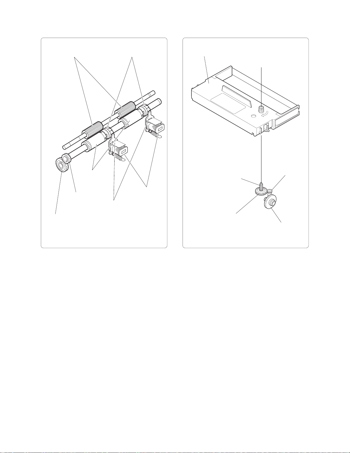
2-3-4 Paper Feed Assembly
g
(1) Paper feed mechanism
2-3-5 Ribbon Cassette Assembly
(1) Ribbon cassette feed mechanism
Pressure rollers
Idling gear 2
PF gear
PF roller
assembly
PF latches
PF armature
PF solenoid
assembly
Ribbon cassette
Ribbon drive shaft
Ribbon drive gear
Worm wheel
Reduction
ear 1
6
Page 91

2-3-6 Paper Take-up Assembly
(1) Paper take-up mechanism
Spool
Winder timing belt
Idle gear 2
(3) Take-up mechanism types
Spool gear
Type which is the same height as the main unit
Spool holder assembly
(2) Near-end detection mechanism
Roll paper
Roll paper core
hole center
(when diameter is large)
Winder pulleys
Type which is lower than the height of the main unit
Microswitch
Roll paper core
hole center
(when diameter is small)
End switch leverSwitch holder
7
Page 92

2-4 Connectors
2-4-2 Terminal Functions
2-4-1 Terminal Layout
Connector type
Printer side: Molex 5342-30T2
Host side: Molex 5320-30AT2
Pin arrangement diagram
29
30
Pin
no.
1
2
3
1
4
5
2
6
7
8
9
10
11
12
13
14
Terminal name Function
Print solenoid #3
Motor (-) VM COM.
VM COM.
Print solenoid #7
Motor on/off signal
Print solenoid COM.
Home position sensor output
Print solenoid COM.
VS
VS
Dot pulse sensor output
Print solenoid #5
Motor (+)
+VM (+24 V)
Print solenoid #2
—
Print solenoid #1
—
Multi-line validation
SOL. (option)
15
16
17
18
19
20
21
22
23
24
25
26
27
28
29
Print solenoid #9
—
Print solenoid COM.
—
Print solenoid #8
Paper feed solenoid (J)
Print solenoid #4
Paper feed solenoid (R)
Print solenoid COM.
GND
Print solenoid #6
Reset pulse sensor output
—
—
+5 V
VS
VS
30
—
8
Page 93

2-4-3 Terminal Circuit Diagram
Print solenoid #3
Motor (-) 24 V GND
Print solenoid #7
Motor ON/OFF signal
Print solenoid COM. (VS)
H.P. (home position pulse)
Print solenoid COM. (VS)
D.P. (dot pulse)
Print solenoid #5
Motor (+) (+24 V)
Print solenoid #2
(reserved)
Print solenoid #1
(reserved)
Print solenoid #9
(reserved)
Print solenoid COM. (VS)
Blank
Print solenoid #8
Paper feed solenoid (J)
Print solenoid #4
Paper feed solenoid (R)
Print solenoid COM. (VS)
GND
Print solenoid #6
RP (reset pulse)
Blank
Blank (RP)
+5 V
Blank
9
Page 94

CHAPTER 3. Disassembly and Assembly
Please observe the following precautions when
performing maintenance.
Note
(1) If the unit is working properly, do not
disassemble, reassemble, or adjust it
unnecessarily. The adjustment screws in
particular should not be loosened needlessly.
(2) After servicing, double-check that the unit
has been assembled correctly before turning
the power on.
(3) Never attempt to print when printer paper is
not loaded.
(4) Verify that the printer paper is loaded
correctly.
(5) When servicing the unit, take care not to
leave any screws or other loose parts in the
unit.
(6) When disassembling and reassembling the
unit, take care not to place strain on any
connecting wires, and check that the wires
are not damaged or routed incorrectly.
(1) Screw nuts on fastening screws (M3x10 hex socket
screws) and insert screws into paper guide (U). Make
sure that nuts fit snugly into V-shaped cutouts on
paper guide (U).
Fastening screw
Nut
Rear
V-shaped cutout
Paper guides (U)
3-1 Required Tools
1. Phillips screwdriver 8. Tester
2. Flatblade screwdriver 9. Oscilloscope
3. Pincette 10. Thickness gauge
4. Mini radio pliers (0.5 mm)
5. Oil brush 11. Dial tension gauge
6. Mini nipper (30 - 50 gf)
7. Hex wrench
(nominal 2.5)
3-2 Disassembly Procedure
Remove the parts from the frame in the opposite
order from the steps described in "3-3 Assembly
Procedure".
3-3 Assembly Procedure
The description of the assembly procedure
assumes that the individual assemblies are
complete. For information on the procedures for
individual assemblies, please refer to "Section 5
Parts List". The part names used in the
explanatory text are those indicated in Section 5
“Parts Lists”. These part names are used
commonly throughout this service manual.
(2) Fit pressure roller springs (L) and (R) onto both sides
of PF housing and set platen assembly in place.
Rear
Pressure roller
spring (L)
Platen assembly
Pressure roller
spring (R)
PF housing
10
Page 95

(3) Fit PF housing with mounted platen assembly into
paper guide (U) and fasten it with fastening screws
(A) (M3x6) and other fastening screw (M3x8).
Note: 1. When performing assembly procedures,
push the PF housing down until it is secured
by the four hooks on the paper guide (U).
2. Tighten the mounting screws (A) only after
adjusting the head gap.
Fastening screw (A)
PF housing
Hooks
Paper guide (U)
Rear
Hooks
(4) Apply Moly LG-S No. 1 to entire clutch spring area
on receipt side of PF shaft.
Note: 1. The PF shaft should have the slit on the
journal side and should not be on the
receipt side.
2. Apply the Moly LG-S No. 1 at about 30
mm from the tip of the receipt side.
(5) Apply Moly LG-S No. 1 to the inside of PF clutch
spring 2 and mount it on the clutch spring section
on the receipt side of the PF shaft.
Note: To facilitate mounting the spring, rotate it
in the direction where the spring
compresses while pushing it in.
(6) Mount PF roller assembly and journal PF latch onto
PF shaft from journal side.
Note: Pay attention to the mounting orientation
of the PF roller assembly and the PF latch.
Receipt side
PF clutch spring 2
Approx. 30 mm
Apply Moly LG-S No. 1
PF shaft
Receipt PF roller assembly
(7) Apply Moly LG-S No. 1 to the entire clutch spring
mounting section on the journal side of the PF shaft.
Note: Apply the Moly LG-S No. 1 at about 60
mm from the tip of the journal side.
(8) Fit the PF clutch spring onto clutch spring section
on journal side of PF shaft.
Note: To facilitate mounting the spring, rotate it
in the direction where the spring
compresses while pushing it in.
(9) Apply Mobile 1 to the PF shaft on the right and left
of the PF clutch springs.
Note: 1. Apply Mobile 1 for a width of about 5 mm,
starting about 10 mm from the right edge
of the PF clutch spring. This is the
mounting position for the PF roller
assembly.
2. The PF latch and PF clutch spring are
different on the receipt side and journal
side.
Receipt side: PF latch 2 (milk white)
PF clutch spring 2 (0.5 mm
dia.)
Journal side: PF latch 2 (black)
PF clutch spring (0.6 mm
dia.)
Journal side
Slit
Journal PF latch
11
Page 96

g
(10) Mount the PF latch 2 onto PF shaft from the receipt
side, and the PF roller assembly from the journal side.
Receipt side
PF latch 2
Journal side
5mm
Apply Mobile 1
PF latch
10mm
PF clutch spring 2
(Apply Moly LG-S No. 1
to outer circumference)
(Apply Moly LG-S No. 1
to outer circumference)
5mm
PF clutch spring
(11) Engage the PF roller assembly, PF latch and PF latch
2 with PF clutch spring and PF clutch spring 2,
respectively.
Note: There are protrusions at both ends of the
PF clutch springs. Match these to the slits
on the PF roller assembly and the PF latch.
5mm
Apply Mobile 1
10mm
5mm
PF roller assembly
(12) Insert the PF shaft assembly into the PF housing
and apply ORELUBE G-1/3 to the left and right
fixing lever (L)and (R).
Note: When mounting the PF shaft assembly,
match the PF roller assembly and PF latch
position to the platen width of the PF
housing.
Apply ORELUBE G-1/3
PF shaft assembly
Platen
Rear
Apply ORELUBE G-1/3
PF housin
PF latch
(PF latch 2)
PF clutch spring
(PF clutch spring 2)
Protrusion
Slit
Protrusion
PF roller assembly
Slit
12
Page 97

(13) Mount fixing levers (L) and (R) and PF gear on to
y
the PF shaft assembly, and fasten with E-rings (E4).
(14) Attach the fixing lever spring to fixing levers (L)
and (R).
(15) Insert the paper guide spring into pressure roller
shaft assembly.
Note: Pressure roller shaft assembly refers to
the pressure roller shaft with mounted
pressure rollers.
(16) While pushing the pressure roller springs (L) and
(R) towards the front side, mount the pressure
roller shaft assembly in the PF housing.
Note: After mounting, verify that the pressure
roller springs (L) and (R) are firmly
engaged in the grooves of the pressure
roller shaft assembly.
(17) Apply FLOIL G-337 to the PF armature tip. Then
mount the PF solenoid assembly to the PF housing
and fasten it with fixing screws (M3x8).
Fixing screws
Apply
FLOIL G-337
PF solenoid
assembly
Rear
PF housing
E-ring
Pressure
roller spring (L)
Fixing
lever spring
PF shaft
assembly
Groove
(Apply ORELUBE G 1/3)
Pressure roller
shaft assembly
(Apply ORELUBE G 1/3)
Fixing
lever (L)
Groove
Fixing lever (R)
Rear
PF housing
Pressure
roller spring (R)
Paper
guide spring
PF gear
E-ring
Fixing
lever spring
(18) Install the pull paper guide to the pressure
roller shaft assembly.
Note: When installing, engage one end of the
paper guide spring in the top right cutout
of the pull paper guide and the other end
in the slit of the PF shaft assembly.
Cutout
Pull paper guide
Rear
Paper guide spring
Pressure roller
shaft assembl
13
Page 98

(
)
(19) Install four paper side guide plates on the bottom
g
of paper guide (U).
(23) Apply ORELUBE G-1/3 to the pivot of the main
frame assembly. Mount the carriage drive gear and
carriage drive pulley and fasten with E-ring (E2.5).
Rear
Paper guide (U)
Paper side
uide plates
(20) Insert the washer and spool spring into the spool
gear assembly and apply Moly LG-S No. 1.
Note: 1. The spool gear assembly refers to the spool
gear with inserted spool spring bush.
2. When installing, the hook of the spool
spring should face forward, and the spring
should be turned counterclockwise.
(21) Apply Moly LG-S No. 1 to the outer circumference
of the spool spring and install the winder pulley.
(22) Apply Moly LG-S No. 1 to the pivot of the spool holder
assembly. Fit the spool gear assembly with the mounted
winder pulley in and fasten it with E-ring (E3).
Carriage drive gear
Main frame
assembly
E-ring
Carriage drive pulley
Apply ORELUBE G-1/3
Pivot
Rear
Pivot
Apply Moly LG-S No. 1
E-ring
Winder pulley
Spool gear
assembly
Spool holder assembly
(Apply Moly LG-S No. 1 )
Washer
Spool spring
14
Page 99

(24) Apply ORELUBE G-1/3 to the pivot of the pulley
drive assembly. Mount the carriage drive pulley and
fasten with E-ring (E2.5).
(25) Align the positions of the mounted carriage drive
pulley cutout and the cutout of the other carriage drive
pulley andmount timing belt assembly.
(26) Provisionally fasten the pulley drive assembly with
M3 washer and fastening screw (M3x5).
(27) Move the carriage drive pin to the center of the pulley
drive assembly, perform the tension adjustment to
determine the position of pulley drive plate assembly,
and fasten the assembly. Use a dial tension gauge
for the tension adjustment. When pushed with a force
of 30 gf, the timing belt displacement must be 2 mm.
(28) Apply ORELUBE G-1/3 to the fastening boss of the
stamp lever plate in the paper guide (L) assembly and
to the three slits contacting the plate.
Note: Paper guide (L) assembly refers to the
paper guide (L) with pressure rollers,
paper pressure sheet, 1-line validation
PCB assembly and validation guide plate
installed.
Rear
Paper guide (L)
assembly
Fastening screw
Washer
Main frame
assembly
Apply
ORELUBE G-1/3
Pulley drive plate assembly
Pulley drive
plate assembly
Position
adjustment
E-ring
Carriage drive pulley
Timing belt
assembly
pin center position
2mm 30gf
Rear
Carriage drive
assembly
Carriage drive
(Apply ORELUBE G-1/3)
Boss
(29) Install the paper guide (L) assembly in the main frame
assembly and fasten with fastening screws (M3x6).
Fastening screw
Stamp lever plate
Paper guide (L)
assembly
Rear
15
Main frame assembly
Fastening
screw
Page 100

y
(30) Mount the motor assembly and motor spacer on to
the right side of the main frame assembly and
fasten with fastening screws (M3x5).
Note: Mount the motor so that the lead wires are
on the bottom side.
Motor assembly
Rear
Motor spacer
Rear
Main frame
assembly
(31) Apply ORELUBE G-1/3 to the three pivots on the
right side of the main frame assembly.
Fastening
screws
Rear
E-ring
Main frame
assembly
Motor gear
Bevel gear 1
Bevel gear 1
pivot
E-ring
(34) Install the idle gear 1 and idle gear 2 and the winder
pulley assembly.
Note: 1. Winder pulley assembly refers to the
winder pulley with the idle gear 2 installed.
2. Mount the winder gear 2 and the winder pulley
assembly while disengaging the securing
hook.
Rear
Winder pulley
assembly
Pivot
Main frame
assembly
(Apply ORELUBE G-1/3)
(32) Mount the motor gear on the shaft of the motor assembly.
(33) Install the bevel gear 1 and fasten with E-ring (E2) over
the bevel gear 1 pivot.
16
Main frame
assembl
Idle gear 2
Securing hook
Idle gear 1
 Loading...