

Page 1
SERVICE MANUAL
POS TERMINAL
MODEL UP-5700
("U" & "A" version)
CONTENTS
WIRING DIAGRAM
CHAPTER 1. SPECIFICATIONS. . . . . . . . . . . . . . . . . . . . . . . . . . . 1-1
CHAPTER 2. OPTIONS. . . . . . . . . . . . . . . . . . . . . . . . . . . . . . . . . . 2-1
CHAPTER 3. SERVICE PRECAUTION. . . . . . . . . . . . . . . . . . . . . . 3-1
CHAPTER 4. DIAGNOSTICS SPECIFICATIONS . . . . . . . . . . . . . . 4- 1
CHAPTER 5. CIRCUIT DESCRIPTION. . . . . . . . . . . . . . . . . . . . . . 5-1
CHAPTER 6. POWER SUPPLY UNIT. . . . . . . . . . . . . . . . . . . . . . . 6-1
CHAPTER 7. BIOS SET UP UTILITY . . . . . . . . . . . . . . . . . . . . . . . 7-1
CHAPTER 8. ABOUT UTILITY SOFTWARE AND OTHERS . . . . . 8-1
CHAPTER 9. CIRCUIT DIAGRAM. . . . . . . . . . . . . . . . . . . . . . . . . . 9-1
CHAPTER 10. PWB LAYOUT . . . . . . . . . . . . . . . . . . . . . . . . . . . . . 10-1
PARTS GUIDE
Parts marked with " " is important for maintaining the safety of the set. Be sure to replace these parts with specified
ones for maintaining the safety and performance of the set.
This document has been published to be used
SHARP CORPORATION
for after sales service only.
The contents are subject to change without notice.
Page 2
THE FOLLOWING CAUTION IS APPLICABLE IN THE UNITED STATES ONLY.
“B A T T E R Y D I S P O S A L”
“CONTAINS NICKEL-CADMIUM RECHARGEABLE BATTERY MUST BE RECYCLED OR DISPOSED OF
PROPERLY. REMOVE THE BATTERY FROM THE PRODUCT AND CONTACT FEDERAL OR STATE
ENVIRONMENTAL AGENCIES FOR INFORMATION ON RECYCLING AND DISPOSAL OPTIONS.”
The RBRCTM Seal
TM
The RBRC
Seal on the easily removabl e nick el-cadmium battery pack contained
in our product indicates that SHARP is voluntarily participating in an industry program to
collect and recycle these battery pac ks at the end of their useful life, when taken out of
TM
service within the United States. The RBRC
program provides a convenient alternative to
placing spent nickel-cadmium battery packs into the trash or municipal waste stream,
which is illegal in some areas.
TM
SHARP’s payments to RBRC
makes it easy for you to drop off the spent battery pack at local retailers
of replacement nickel-cadmium batteries, or at authorized SHARP product service centers. You may also contact
your local recycling center for information on where to return the spent battery pack. SHARP’s involvement in this
program is part of its commitment to protecting our environment and conserving natural resources.
TM
(RBRC
is a trademark of the Rechargeable Battery Recycling Corporation.)
Page 3
CHAPTER 1. SPECIFICATIONS
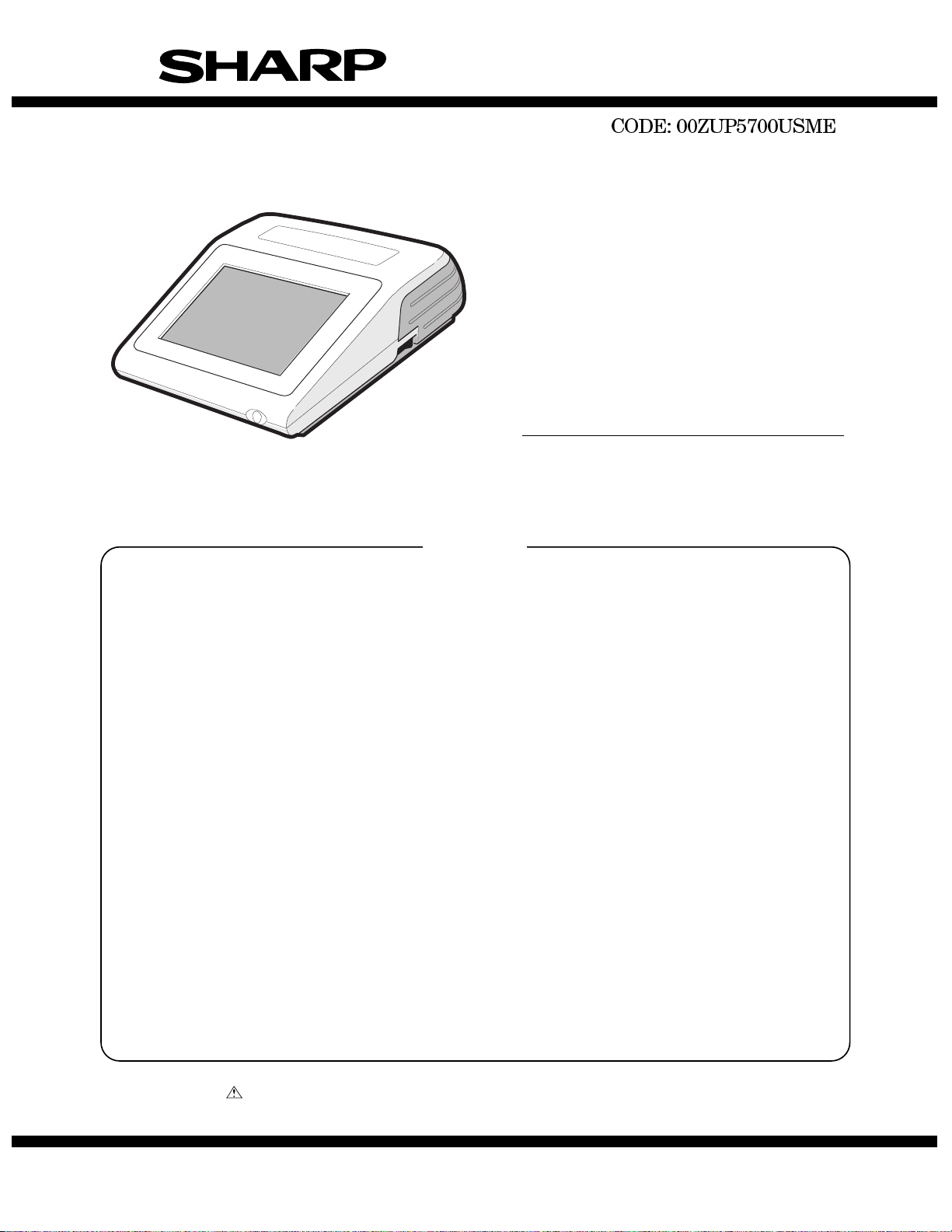
1. Appearance
Flat-panel LCD display
with touch-sensitive overlay
Power switch
AC cord
Plug your POS terminal into a wall outlet before using.
Power switch
Set the power switch to the ON ( I ) position after plugging your POS
terminal.
2. Rating
ITEM SPECIFICATIONS
External dimensions 290 (W) ´ 365 (D) ´ 131 (H) mm
Weight 5.5 kg
Power source Official (normal) voltage and
Power consumption Operating: 43 W
Working temperature and
humidity
frequency
0 to 40°C (32 to 104°F)
10 to 90%
3-3. PC system
ITEM SPECIFICATIONS NOTE
CPU Pentium processor
Chip set OPTI 82C700
VGA chip C&T T65550B
Main memory
(for executing MS-DOS,
Application software)
Video RAM 1 Mbytes EDO type
BIOS ROM 512 Kbytes Flash ROM
OS (MS-DOS) ROM 4 Mbytes Mask ROM
ROM disk memo r y
(for stored Application
software)
RAM disk memory
(for POS data)
Key controller M38802
Super I/O M5113
Standard: 8 Mbytes EDO type
Max.: 40 Mbytes adding S.O.DIMM
Standard: 2 Mbytes Flash ROM
Max.: 6 Mbytes adding UP-F04RB
Standard: 1 Mbytes
Max.: 3 Mbytes adding UP-P02MB
3-4. Serial port
D-SUB 9-pin connector COM1 and COM2 are equipped.
In order to supply +5V power, CI signal and +5V power supply of
COM1 and COM2 can be switched.
2 channels of RJ45 Connector COM port are equipped.
COM3 and COM4 or original I/O address (COM5 and COM6) can be
selected as the 2 channels of RJ45 COM port.
COM1 & COM2: D-sub 9 pin
Pin No. Signal Function I/O
1 CD Data Carrier Detect I
2 RD Receive Data I
3 SD Send Data O
4 ER Data Terminal Ready O
5 SG Signal Ground —
6 DR Data set Ready I
7 RS Request to Send O
8 CS Clear to Send I
9 CI/+5V Ring Indicate / +5V I/–
3. Hardware
3-1. Display
ITEM SPECIFICATIONS NOTE
Type TFT color LCD with back
Screen size 10.4" Full screen
Dot format 640 (W) ´ 480 (H) dots
Dot size 0.33 ´ 0.33 mm
Control VGA
3-2. Keyboard
ITEM SPECIFICATIONS NOTE
Type Touch key
Number of key
positions
Control Mouse emulation
light
(Analog touch panel)
4096 (W) ´ 4096 (H)
positions
With 256 colors
COM3 or COM5: Modular jack RJ45 8 pin
Pin No. Signal Function I/O
1 RS Request to Send O
2 ER Data terminal Ready I
3 SD Send Data O
4 SG/(+5V) Signal Ground/(+5V) —
5 SG Signal Ground –
6 DR Receive Data I
7 DR Data set Ready I
8 CS Clear to Send I
1 – 1
Page 4
COM4 or COM6: Modular jack RJ45 8 pin
Pin No. Signal Function I/O
1 RS Request to Send O
2 ER Data terminal Ready I
3 SD Send Data O
4 SG Signal Ground —
5 SG Signal Ground –
6 RD Receive Data I
7 DR Data set Ready I
8 CS Clear to Send I
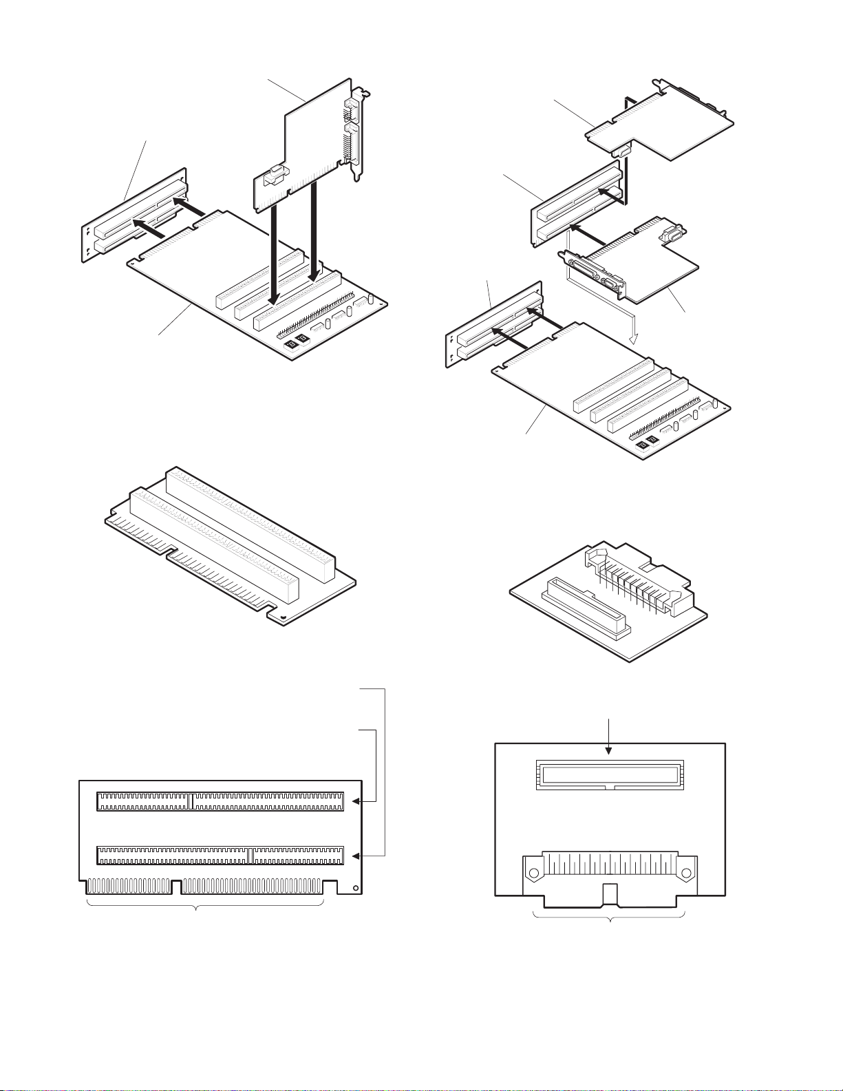
3-5. Expansion slot
ITEM SPECIFICATIONS NOTE
Type ISA bus Half size PC board
Number of slots 2 slots
Power consumption +5V/max. 1.0A
+12V/max. 0.05A
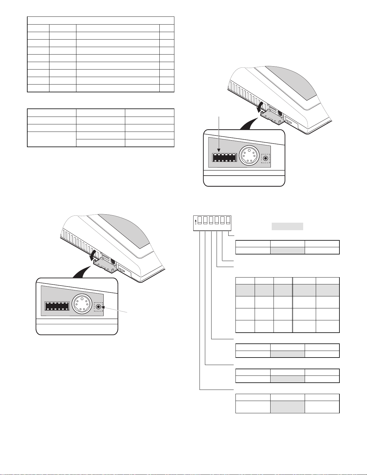
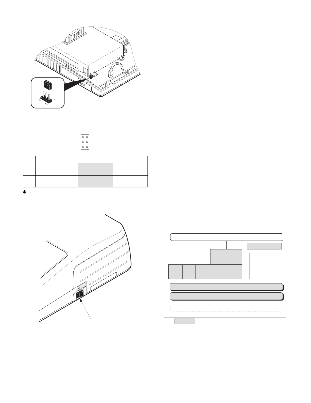
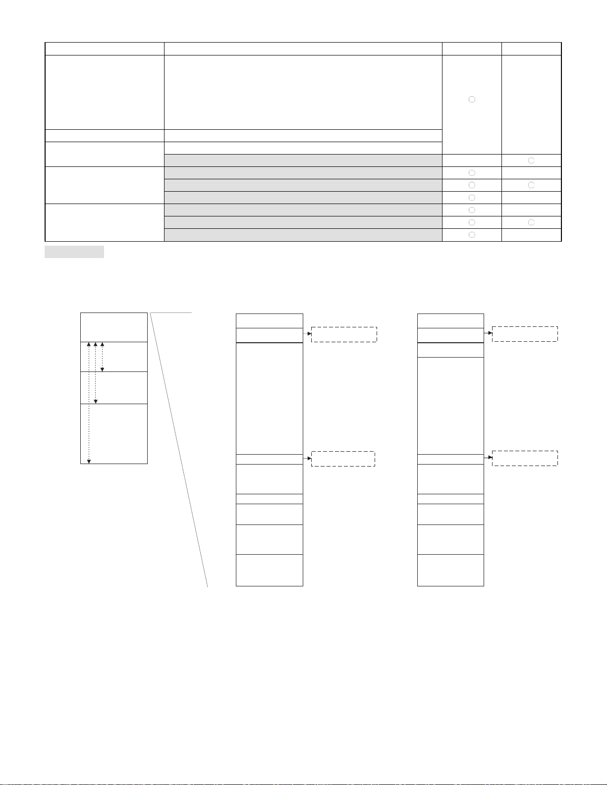
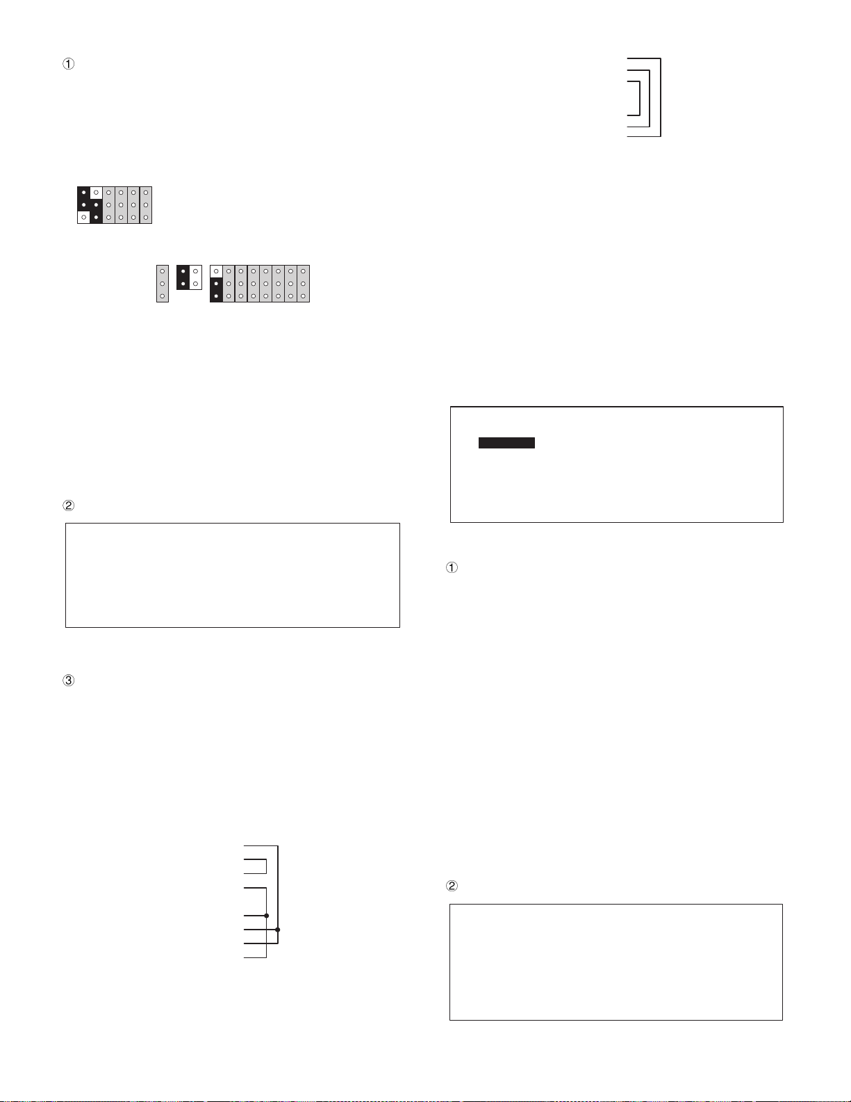
3-7. System switch
The system switch is used to preset for system configuration.
[Out line]
The system switch is consist of DIP switch and Jumper switch.
[DIP switch]
System switch
3-6. Shutdown switch
Shutdown switch used when the OS or application programs are
straying and the system can not return to the normal state.
You must not use this shutdown switch when t he UP-5700 is running
normally. Use this switch only when the main power source is not cut
off even if the main unit power switch is set to OFF position. UP-5700
is turned OFF and the hardware is reset by turning the main power
switch OFF and then pressing the shutdown switch.
123456
Shut down switch
123456
The PSC2 simply reads switched signals from the DIP switch as
hardware. The meaning of DIP switch wholly depends on the software.
ON
123456
ON
OFF
: Default setting
DSW-6
Function OFF (value = 1) ON (value = 0)
CMOS Initialize Not Initialize Initialize
DSW-5
DWS-4
Drive C:, D: & E: Setting
Drive C: Drive D: Drive E: SW-4 SW-5
Flash
PS RAM HDD
ROM
HDD — —
HDD PS RAM
PS RAM
Flash
ROM
Flash
ROMON(value = 0)
HDD
OFF
(value = 1)
ON
(value = 0)ON(value = 0)
OFF
(value = 1)ON(value = 0)
OFF
(value = 0)
OFF
(value = 1)
[Out line]
The shutdown switch is single shot type. (Normally OFF position)
Push ON: This position is used to reset stand-by mode for power
supply unit when software hang up.
Release OFF: Usually the shutdown switch needs to be set to this
position when the UP-5700 is operated.
[Operating method]
The shutdown switch is a push switch. If it is push ON, UP-5700
performs to stop supplying the power when t he power switch is set
into stand-by mode.
NOTE: The shutdown operation will be ignore when te power switch
is set into power-on position.
1 – 2
DSW-3
Function OFF (value = 1) ON (value = 0)
Boot Drive Drive A: Drive C:
DSW-2
Function OFF (value = 1) ON (value = 0)
Drive A: Device Mask ROM FDD
DSW-1
Function OFF (value = 1) ON (value = 0)
Floppy Disk
Controller
Not Exit Exit
Page 5
[Jumper switch]
Jumper switches the following functions for UART1 and UART2 in the
PSC2.
8 7
ON
OFF
SW Function OFF (value = 1) ON (value = 0)
7COM3 & COM4 IRQ
assign
8 G/A UART1&2
decode mode
COM3 = IRQ11 COM3 = IRQ4
COM4 = IRQ10 COM4 = IRQ3
COM3 & COM4 COM5 & COM6
When SW8 is set to ON, the setting of SW7 is not valid.
3-8. Power switch
[Out line]
The power switch has the positions ON and OFF (Stand-by)
ON position: Usually the power switch needs to be set to t his posi-
tion when the POS-terminal is operated.
OFF position: This position is used to turn the stand-by mode. When
the power switch is set to this position, power supply
stops automatically. But if the soft ware program control the power supply to hold, even if the power switch
is set into this position, power supplying will be kept
until an software program allows power supply no to
hold.
[Operating method]
The power switch is a seesaw switch, and it can be tipped toward the
ON or OFF.
4. Software
4-1. Software Structure
The basic system software is mainly consisted of the following 3
modules.
(1) MS-DOS Version 6.22
The operating system (MS-DOS Version 6.22) is stored in MROM
disk.
(2) Drivers
There are following types of drivers
· POS Device Driver (for Clerk, Buzzer, Drawer, Timer, MCR, Line
Display, Serial Port) POS device drivers adopt same control
method as the control of former (ER-A850/A880) software.
· SRN Driver
· Touch Panel Driver
(3) POS Device Middleware
Middleware helps improve development of applications.
(4) Software Structure
Power switch
The power switch is used to turn the POS terminal on or stand-by
If the communication function is used, the AC power can be turned off
by software operation for power saving after communication.
SRN
Driver
Touch
Panel
Driver
Application
POS Device
Mifddle Wsre
DOS Devlce Driver
MS-DOS Version 6.22
BIOS
Hardware
Provided from SHARP
POS Utillty
Standard PC
Device Driver
(Local production)
SCSI
Ethernet
.......etc
1 – 3
Page 6
4-2. Basic system software list
ITEM CONTENTS for UP-5700 for PC
BIOD (FROM)
· AT compatible system BIOS
· VGA BIOS for C&T65550 VGA LSI
· Standard SETUP program
· Flash Disk/MROM Disk/PSRAM Disk built-in control program
· Memory size/HDD type auto detect function
· No APM/PnP support
OS (MROM disk) MS-DOS Version 6.22 (Subset)
Install program (MROM disk)
· System Install program
· APL Install program (for MS-DOS/Windows 95) —
POS device driver · POS device driver —
· SRN driver
· Touch panel driver (mouse emulation I/F only) —
Middleware soft and
application development tools
· POS device MiddleWare —
· R/J Logo image loading utility program (MS-DOS/Windows 95)
· Touch panel calibration utility program (MS-DOS) —
... These software are provided with FD from SHARP.
Please copy contents of FD provided from department to development PC. Install to UP-5700 by using APL Install Program from PC.
4-3. Memory map
—
0000000h
STD. 8MB
0800000h
+8MB
1000000h
1800000h
2800000h
(16MB)
+8MB
(24MB)
+32MB
(40MB)
Memory is expandable up to
32MB using EMM386 in DOS.
00000h
9F4000h
A0000h
C0000h
CB000h
E8000h
100000h
MS-DOS
(25K)
Sharp Driver
(32K)
Free
Conventional
(580K)
EBDA : 3K
VRAM
128K
VGA BIOS(40K)
UMB
(116K)
System BIOS
(96k)
HMA
64K
Not Use Middleware
POS Device 20K
Touch Key 12k
(External BIOS
Data Area)
00000h
9F4000h
A0000h
C0000h
CB000h
E8000h
100000h
MS-DOS
(25K)
Sharp Driver
(32K)
Middleware
(15K)
Free
Conventional
(565K)
EBDA:3K
VRAM
128K
VGA BIOS(40K)
UMB
(116K)
System BIOS
(96k)
HMA
64K
Use Middleware
POS Device 20K
Touch Key 12k
(External BIOS
Data Area)
1 – 4
Page 7
CHAPTER 2. OPTIONS
1. System configuration
AT Keyboard
<supplied on site>
Drawer
<Option>
ER-03DW/
04W/05DW
Customer
Poll Display
<Option>
UP-P20DP
In-line Communication
Connection
Incorporated in Main Unit
max.2
Additional
RAM Memory
<Option>
UP-P02MB
Additional
ROM Memory
<Option>
UP-F04RB
Additional DRAM
Memory
<supplied on site>
Magnetic
Card Reader
<Option>
UP-E12MR
Customer
Display
<Option>
ER-A8DP
HDD Unit
<supplied on site>
Master Machine
UP-5700
(RS-232)
RS232 Board
<Option>
ER-A8RS
SRN Board
<Option>
ER-01IN-PC
Ethernet Board
<supplied on site>
Centronics Printer
<supplied on site>
RS-232 Communication Connection
max.6
Hand Scanner
Remote Printer
<Option> ER-01PU
<supplied on site> TM-T80/85/295
ER-FBT40
<Option>
ER-A6HS1
Satellite Machine
UP-5700
2. Options
No. NAME MODEL NAME DESCRIPTION
1 Expansion RAM disk board UP-P02MB 2 Mbytes RAM board
2 Expansion ROM disk board UP-F04RB 4 Mbytes ROM board
3 Customer display ER-A8DP 1 line 7-segments display
4 Customer pole display UP-P20DP 2 line 20 digits dot display
5 MCR (Magnetic Card Reader) UP-E12MR for ISO 1 & 2 stripe card
6 Remote drawer ER-03DW
ER-04DW
ER-05DW
7 PC-SRN board ER-01IN-PC SRN communication board for ISA bus slot
8 RS232 & CENTRO I/F board ER-A8RS RS232 9 pins connector: 2 ports
CENTRONICS 25 pins connector: 1 port
9 Receipt/Journal printer ER-01PU 2 station (R/J) printer
10 Hand scanner ER-A6HS1 for reading bar code
2 – 1
Page 8
3. Service options: None
No. NAME PARTS CODE
1 HDD kit
4. Service tools
No. NAME PARTS CODE PRICE DESCRIPTION
1 Service tool kit
2 Printer connector signal loop back connector
3 MCR test card
4 RS232 loop back connector
5 CPU/VGA PWB relay PWB
6 BIOS loading board
7 RS232 modular jack loop back connector
8 BIOS MASTER ROM
9 TOUCH PEN
*
1 Always use this pen for the TOUCH PANEL POSITION ADJUSTING UTILITY PROGRAM.
This pen is for K-PDA (ZR-xxxx series).
If you use a ball-point pen or other pens whose point is hard, the surface of TOUCH PANEL may be damaged.
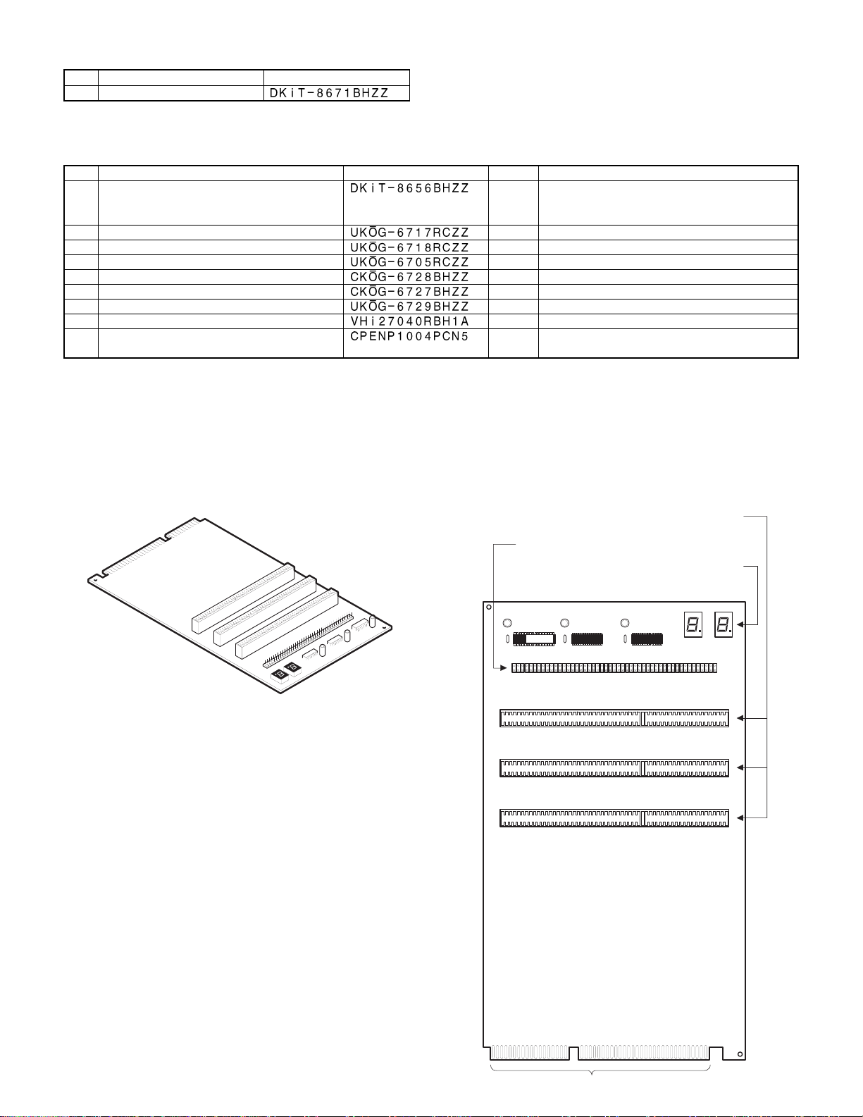
4-1. Service tool kit: DKIT-8656BHZZ
1) ISA checker
Used to repair or check the operation of the optional I/F.
· External view · Plan view
CW ISA checker
ISA relay board
RAM relay board (Not used for UP-5700)
BR for ER-A8RS CENTRONICS connector
BE for UP-E12MR
BC for RS232 connector
CQ
CS for overwriting BIOS
AZ for RJ45 connector
(P) EP-ROM for overwriting BIOS
AG For TOUCH PANEL POSITION ADJUSTING
UTILITY PROGRAM *1
ISA bus connectors:
Used to connect with the I/F PWB of ER-A8RS,
ER-01IN-PC etc.
Test pins: Used to check the ISA bus signal.
LED circuit: Not used currently.
RAM1A
2 – 2
Connected to the ER-A850/A880 ISA bus connectors.
Page 9
· Connection diagram
· Connection diagram
ER-A8RS
(or ER-01IN-PC)
UP-5700
ISA bus connector
ISA checker
2) ISA relay board
Connected to the ISA checker for installation of the optional I/F horizontally and for repairing and checking the operation .
· External view
ER-A8RS (or ER-01IN-PC)
solder side
ISA relay board
ISA PWB
ER-A8RS (or ER-01IN-PC)
parts side
ISA checker
· Plan view
ISA bus connector:
Used to check the ER-A8RS (or ER-01IN-PC)
parts side.
ISA bus connector:
Used to check the ER-A8RS (or ER-01IN-PC)
solder side.
3) RAM PWB relay board (UP-5700: Not used)
· External view
· Plan view
Connected to the ISA bus connector of ISA checker.
2 – 3
Page 10
4-2. Printer connector signal loop check cable:
UKOG-6717RCZZ
Connected to the centronics connector (25 pin) of the ER-A8RS, and
used to check loop signals when executing diagnostics.
· External view
· Plan view and connection diagram
150±8
4-3. MCR test card: UKOG-6718RCZZ
Used when executing the diagnostics of the UP-E12MR.
·
· External view
4-4. RS232 loop back connector: UKOG-6705RCZZ
Connected to the RS232 connector (D-SUB 9 pin: COM1, COM2,
COM3, COM4) of the UP-5700 and ER-A8RS, and used to check
loop signals when executing diagnostics.
· Connection diagram
Signal name Pin No.
1STROBE2DB0
3DB1
4DB2
5DB3
6DB4
7DB5
8DB6
9DB7
10ACK11BUSY
12PE
13SLCT
14AUTOFD15ERROR16INIT17SLCTIN-
18~25PE
· Connection diagram
Signal namePin No.
1 STROBE2DB0
3DB1
4DB2
5DB3
6DB4
7DB5
8DB6
9DB7
10 ACK11 BUSY
12 PE
13 SLCT
14 AUTOFD15 ERROR16 INIT17 SLCTIN-
18~25 PE
CD 1pin
RD 2pin
TD 3pin
DTR 4pin
GND 5pin
DSR 6pin
RTS 7pin
CTS 8pin
RI 9pin
4-5. RS232 modular jack loop back connector:
UKOG-6729BHZZ
Connected to the RS232 connector (RJ45: COM5, COM6) of the
UP-5700 and ER-A8RS, and used to check loop signals when executing diagnostics.
· Connection diagram
RTS
1pin
DTR
2pin
TD
3pin
GND
4pin
GND
5pin
RD
6pin
DSR
7pin
CTS
8pin
ER-A8RS
2 – 4
Page 11
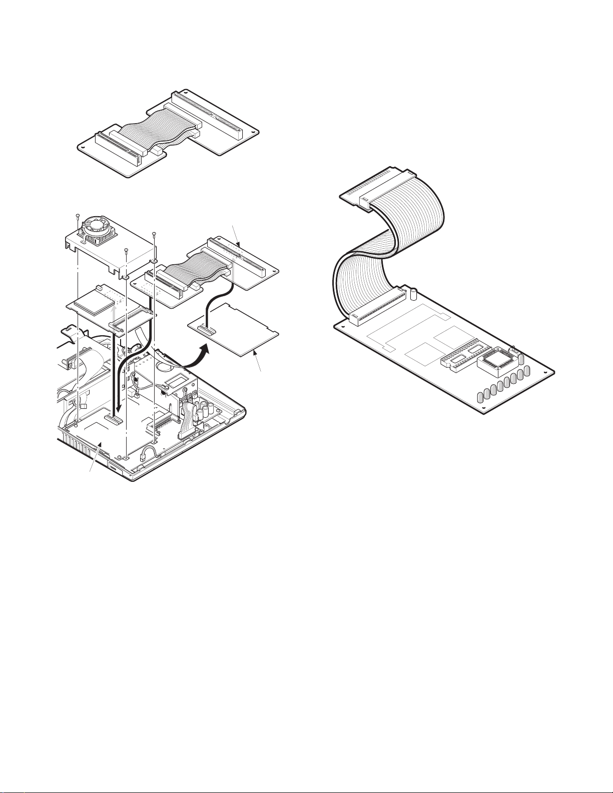
4-6. CPU/VGA PWB relay PWB: CKOG-6728BHZZ
The CPU PWB, you can check the soldered face of the CPU PWB by
connecting the CPU PWB to the VGA PWB.
· External view
· Connection diagram
CPU/VGA PWB relay PWB
4-7. BIOS loading board: CKOG-6727BHZZ
The BIOS loading board: CKOG-6727BHZZ is a tool to write a BIOS
ROM program in the F-ROM on the UP-5700’s main board. Use this
PWB in the following cases:
· The F-ROM on the UP-5700’s main board is changed due to some
defect and a BIOS ROM program is written in the F-ROM.
· The BIOS ROM program in the F-ROM is overwritten due to the
version up of BIOS ROM program, etc.
Connected to the Option ROM/RAM disk connector (CN19) of the
Main PWB.
· External view
Main PWB
CPU PWB
2 – 5
Page 12
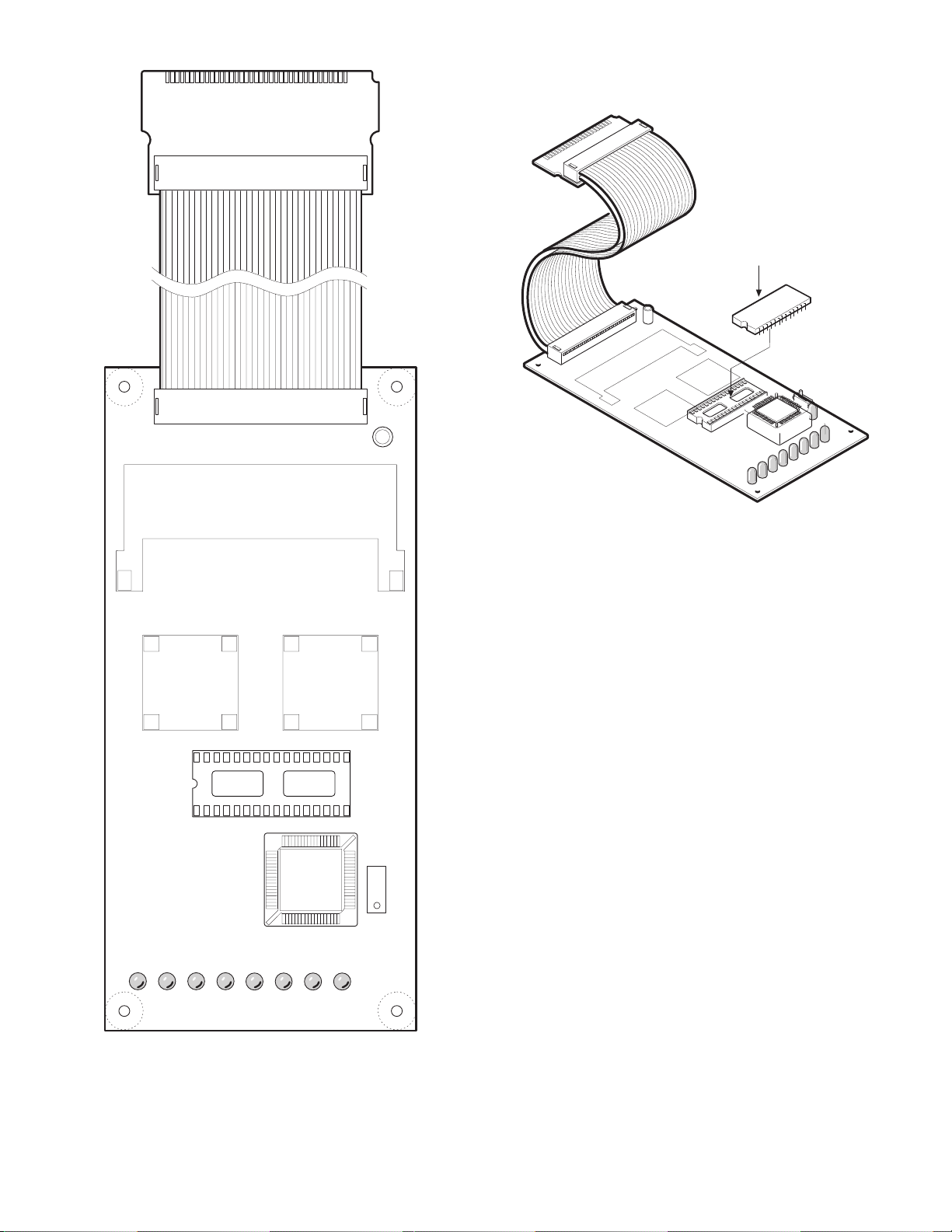
· Plan view
Writing BIOS ROM Program
1. Install the EP-ROM (master ROM): VHI27040RBH1A containing a
BIOS program on the BIOS loading board: CKOG-6727RCZZ.
BIOS MASTER ROM
LED1 LED2 LED3 LED4 LED5 LED6 LED7 LED8
· Connection diagram
SW1
13
2 – 6
Page 13
2. Set SW1 on the BIOS loading board to the side of pin 3.
4. Connect the BIOS loading board to the option ROM/RAM connector CN19 on the main PWB, and then close the cabinet.
LED1 LED2 LED3 LED4 LED5 LED6 LED7 LED8
3. Open the upper cabinet.
SW1
SW1
1
3
LED9
5. Writing the BIOS ROM program starts by turning on the power
switch on the right side.
For the status of LED on the special service PWB when a BIOS
ROM program is being written, see the following table.
Writing is complete (automatic completion) when the green LED
(LED9) on the BIOS loading board lights up.
SW1
1
3
6. After writing is complete, turn off the power switch on the right
side to remove the BIOS loading board, and turn on the power
switch on the left side again to check whether the BIOS program
starts up normally or not.
2 – 7
Page 14
LED DISPLAY STATUS
[ : ON (Lighting) — : OFF]
<In normal operation>
LED1
(RED)
————
—————
————
————
—
———
—
——————
——————
—
———
—
————
LED2
(RED)
——— — — — Programming: Bank0 D0000 h (64KB)
—— — — — Programming: Bank1 D0000 h (64KB)
————— — — Verifying: Bank0 D0000 h (64KB)
—— —— — — Verifying: Bank1 D0000 h (64KB)
LED3
(RED)
—— — — — Programming: Bank0 E0000 h (64KB)
—— — — — Programming: Bank0 F0000 h (64KB)
— — — — Programming: Bank1 E0000 h (64KB)
— — — — Programming: Bank1 F0000 h (64KB)
———— — — Verifying: Bank0 E0000 h (64KB)
———— — — Verifying: Bank0 F0000 h (64KB)
— —— — — Verifying: Bank1 E0000 h (64KB)
— —— — — Verifying: Bank1 F0000 h (64KB)
LED4
(RED)
LED5
(RED)
—— — — Verifying: Bank1 C0000 h (64KB)
LED6
(RED)
LED7
(RED)
————Start initializing
— — — Erasing F-ROM (LED6: RED is blinking)
———
— — — Programming: Bank0 C0000 h (64KB)
— — — Programming: Bank1 C0000 h (64KB)
— — — Setting protection the F-ROM
LED8
(RED)
— — Start verifying the program in the F-ROM
— — Verifying: Bank0 C0000 h (64KB)
LED9
(GREEN)
— Start of COPY FUNCTION
Start copy programming to F-ROM from EPROM
END of complete COPY FUNCTION
FUNCTION
<Erase ERROR in F-ROM>
LED1
(RED)
—
——
<Programming ERROR in F-ROM>
LED1
(RED)
—
<Verifying ERROR in F-ROM>
LED1
(RED)
—
LED2
(RED)
———— — — Device not ready
LED2
(RED)
——— — — Device not ready
LED2
(RED)
——— — — Device not ready while release the protection
LED3
(RED)
——— — — VPP error
——— — — Command sequence error
LED3
(RED)
—— — — VPP error
—— — — Command sequence error
LED3
(RED)
—— — — Can not release the protection
LED4
(RED)
—— — —
LED4
(RED)
LED4
(RED)
LED5
(RED)
LED5
(RED)
LED5
(RED)
LED6
(RED)
LED6
(RED)
LED6
(RED)
LED7
(RED)
LED7
(RED)
LED7
(RED)
LED8
(RED)
LED8
(RED)
LED8
(RED)
LED9
(GREEN)
LED9
(GREEN)
LED9
(GREEN)
FUNCTION
FUNCTION
FUNCTION
2 – 8
Page 15
CHAPTER 3. SERVICE PRECAUTION
1. Conditions for soldering circuit parts
To solder the following parts manually, follow the conditions described below.
PARTS NAME PARTS CODE LOCATION CONDITIONS FOR SOLDERING
Ceramic oscillator
DIP SWITCH
MAIN PWB: X1 (8M) 270°/3sec.
MAIN PWB: X2 (24M)
MAIN PWB: X2 (7.37M)
MAIN PWB: S3 3000°/3sec.
2. Cautions on handling CPU and POWER
FAN
When removing or performing any other operation on the CPU and
POWER FAN, be sure to handle them with care, because it may
cause abnormal sound or deteriorate the performance while the CPU
FAN is rotating if they are dropped or given heavy impact.
3. Note for handling of Touch panel
· The transparency of the touch panel should be vitally important.
Do not put finger prints or wat er print on the surface. Use clean
finger such or gloves and masks.
· For handling, do not hold the transparent are, and do not hold the
heat seal connector section to assure reliability.
· Do not overlay touch panels. The edge may damage the surface.
· Do not put a heavy thing on the touch panel.
· Do not apply a strong shock, and do not drop it.
· When attaching the protection film again, carefully check for no
dirt. If there is any dirt, it is transferred.
· To clean dirt on the surface, use dry, soft cloth or a cloth immersed
in ethyl alcohol.
· Check that the housing does not give stress to the touch panel.
· Be careful not to touch the touch panel with tools.
· The heat seal section is easily disconnected. Be careful not to give
a stress to the heat seal section when installing.
· The touch panel is provided with an air groove to make the exter-
nal and the internal air pressure equal to each other. If water or oil
is put around the air groove, it may penetrate inside. Be careful to
keep the air groove away from water and oil.
· Input is performed with fingers. Do not use a hard thing for input-
ting.
4. Note for handling of LCD
· The LCD elements are made of glass. BE careful not to give them
strong mechanical shock, or they may be broken. Use extreme
care not to break them.
· If the LCD element is broken and the liquid is leaked, do not lick it.
If the liquid is attached to your skin or cloth, immediately clean with
soap.
· Use the unit under the rated conditions to prevent against damage.
· Be careful not to drop water or other liquid on the display surface.
· The reflection plate and the polarizing plate are easily scratched.
BE careful not to touch them with a hard thing such as glass,
tweezers. Never hit, push, or rub the surface with hard things.
· When installing the unit, be careful not to apply stress to the LCD
module. If an excessive stress is applied, abnormal display or
uneven color may result.
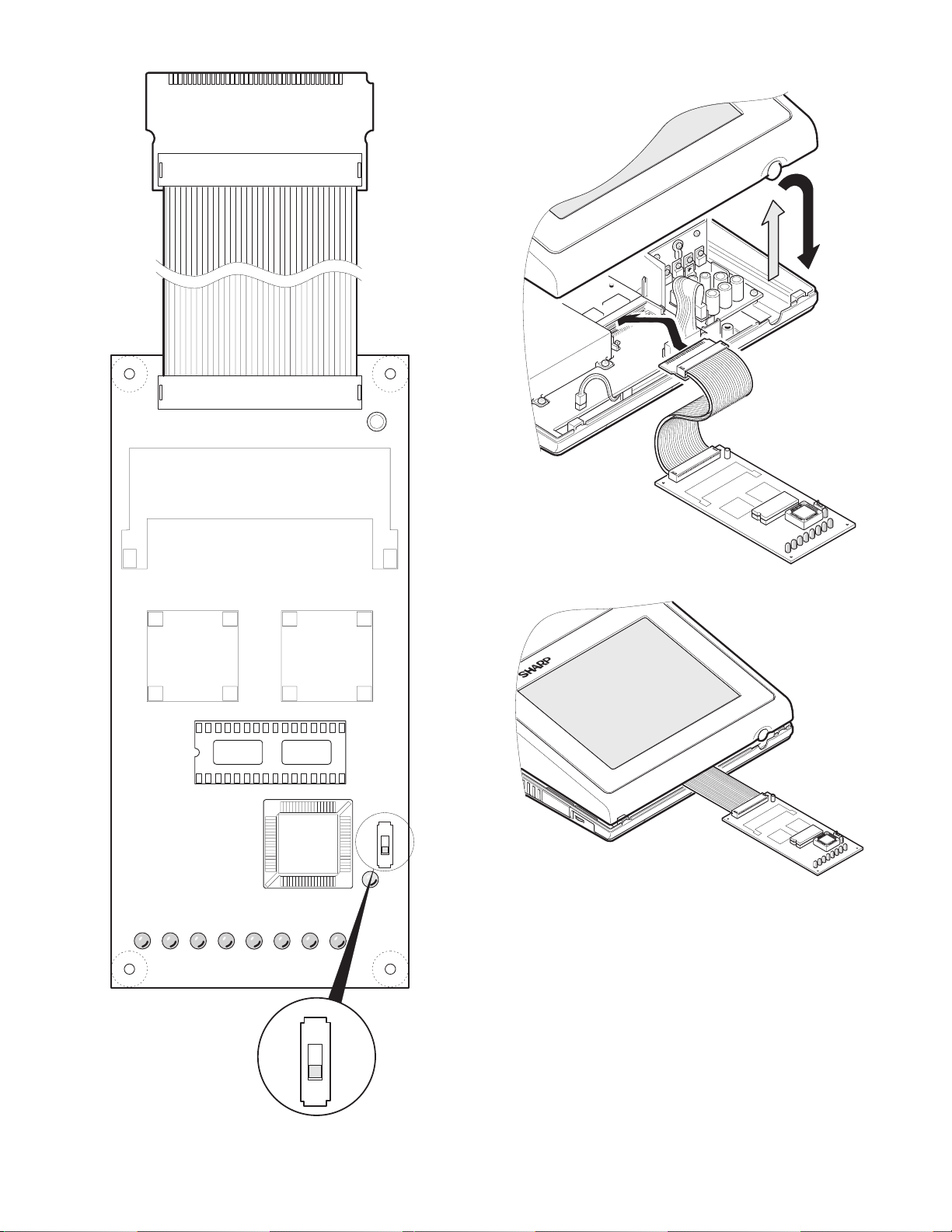
5. Cautions on handling connectors
When connecting or disconnecting the following connectors, follow
the procedures below.
1)
PARTS NAME PARTS CODE LOCATION
FFC
CONNECTOR
· How to Connect or Disconnect FFC
(1) Open the slider to unlock position
The slider will open only up to a fixed height (about 1.2mm). If
you forcibly pull up the slider further, it may be dropped.
UNLOCK
Slider
MAIN PWB: CN12
KEY I/F PWB: CN8/CN10
3 – 1
1.2mm
Page 16
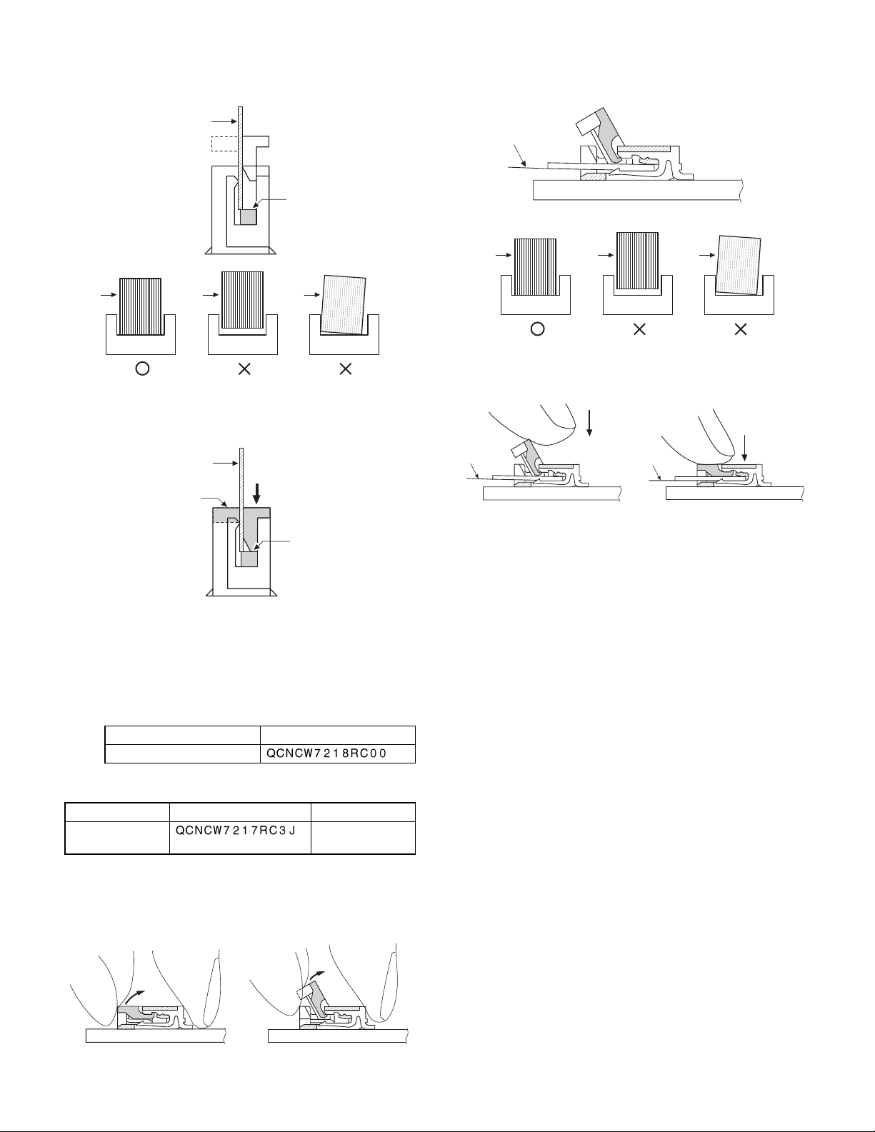
(2) Insert the FFC
Insert the FFC firmly untill the FFC hits the bottom of the connector’s insulator.
FFC
(2) Insert the FFC
Insert the FFC firmly until the FFC hits the bottom of the connector’s insulator.
FFC
FFC
CONNECTOR
FFC
CONNECTOR
FFC
CONNECTOR
(3) Close the slider to lock position
Insert the FFC and then push the slider downward.
FFC
Slider
LOCK
(4) To pull out the FFC, unlock the slider to pull it out in the same
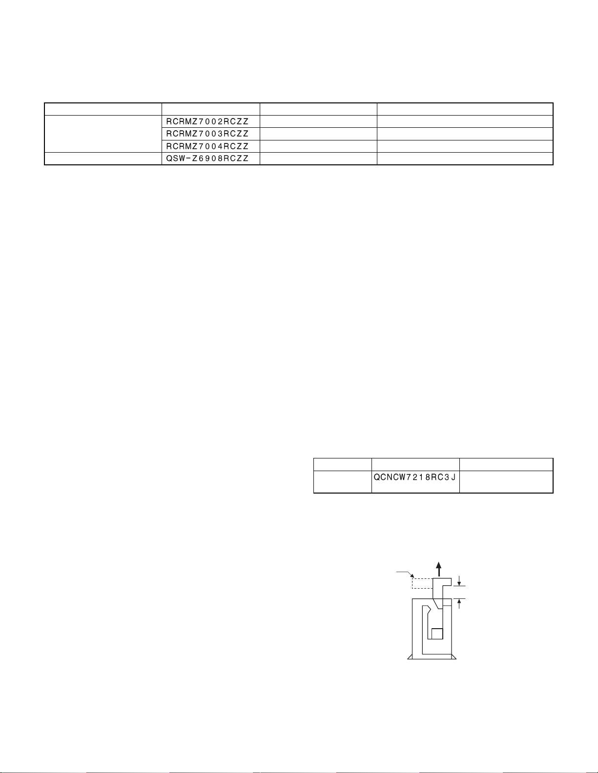
procedures as (1).
· Replacement parts required when the OCNCW7218RC3J’s
slider is broken
Forcibly pulling up the slider further may cause the slider to
drop and to be broken in the worst case. You can change this
slider part only .
PARTS NAME PARTS CODE
SLIDER
2)
PARTS NAME PARTS CODE LOCATION
FFC
CONNECTOR
LCD RELAY
PWB: CN1
FFC
CONNECTOR
FFC
CONNECTOR
FFC
CONNECTOR
(3) Close the slider to lock position
Insert the FFC and then push the slider downward.
FFC
FFC
(4) To pull out the FFC, unlock the slider to pull it out in the same
procedures as (1).
6. AT Keyboard usable for UP-5700
Do not use the following keyboards because they do not work when
connected to the UP-5700.
The UP-5700 can be externally connected to a keyboard.
The UP-5700’s key BIOS conforms to the PC standard, but this
BIOS’s operation is not assured for some keyboards.
Some keyboards may cause operation errors due to delicate timing.
It is currently found out that t he following models of keyboards may
malfunction.
When selecting a keyboard to be connected, operate the keyboard in
advance to check that it correctly works.
· Japanese keyboard (106 keys)
Manufactured by IBM: TYPE/MODEL5576-B01 FRUPN66G0507
· English keyboard (101 keys)
Manufactured by NMB Technologies Inc.: Model: RT6651T+
· How to Insert FFC
(1) Open the slider to unlock position
Open the slider upwards up to an angle of 60 degrees. If the
slider does not fully open, the FFC can not be smoothly inserted.
3 – 2
Page 17
CHAPTER 4. UP-5700
DIAGNOSTICS SPECIFICATIONS
CONTENT
1. General . . . . . . . . . . . . . . . . . . . . . . . . . . . . . . . . . . . . . . . . . . . . 1
2. System configuration. . . . . . . . . . . . . . . . . . . . . . . . . . . . . . . . . . 1
3. Service diagnostics . . . . . . . . . . . . . . . . . . . . . . . . . . . . . . . . . . . 1
3-1. Service diagnostics getting started . . . . . . . . . . . . . . . . . . 1
3-2. Selection menu. . . . . . . . . . . . . . . . . . . . . . . . . . . . . . . . . 2
3-3. RAM Diagnostics . . . . . . . . . . . . . . . . . . . . . . . . . . . . . . . 2
1) D-RAM Check . . . . . . . . . . . . . . . . . . . . . . . . . . . . . . 2
2) Standard RAM Disk Check . . . . . . . . . . . . . . . . . . . . 2
3) OPTION RAM DISK Check . . . . . . . . . . . . . . . . . . . . 3
3-4. ROM Diagnostics . . . . . . . . . . . . . . . . . . . . . . . . . . . . . . . 3
1) DOS ROM Check. . . . . . . . . . . . . . . . . . . . . . . . . . . . 3
2) BIOS ROM Check . . . . . . . . . . . . . . . . . . . . . . . . . . . 3
3) Standrad FLASH ROM Check . . . . . . . . . . . . . . . . . . 4
4) Option FLASH ROM Check . . . . . . . . . . . . . . . . . . . . 4
3-5. Real time clock & CMOS RAM Diagnostics . . . . . . . . . . . 4
1) Real time clock Check . . . . . . . . . . . . . . . . . . . . . . . . 4
2) CMOS RAM Check . . . . . . . . . . . . . . . . . . . . . . . . . . 4
3-6. Touch Panel Diagnostics . . . . . . . . . . . . . . . . . . . . . . . . . 5
1) Controller Diag Test . . . . . . . . . . . . . . . . . . . . . . . . . . 5
2) Touch Key Pad Test . . . . . . . . . . . . . . . . . . . . . . . . . 5
3) Linearity Test . . . . . . . . . . . . . . . . . . . . . . . . . . . . . . . 6
3-7. Clerk Key Diagnostics. . . . . . . . . . . . . . . . . . . . . . . . . . . . 6
1) Clerk Key Check . . . . . . . . . . . . . . . . . . . . . . . . . . . . 6
3-8. Printer Diagnostics . . . . . . . . . . . . . . . . . . . . . . . . . . . . . . 6
1) PARALLEL1 Loop Check. . . . . . . . . . . . . . . . . . . . . . 6
2) PARALLEL2 Loop Check. . . . . . . . . . . . . . . . . . . . . . 7
3) PARALLEL3 Loop Check. . . . . . . . . . . . . . . . . . . . . . 7
4) PARALLEL1 Print Check . . . . . . . . . . . . . . . . . . . . . . 8
5) PARALLEL2 Print Check . . . . . . . . . . . . . . . . . . . . . . 8
6) PARALLEL3 Print Check . . . . . . . . . . . . . . . . . . . . . . 8
3-9. Serial I/O Diagnostics . . . . . . . . . . . . . . . . . . . . . . . . . . . . 8
1) COM1 Check . . . . . . . . . . . . . . . . . . . . . . . . . . . . . . . 9
2) COM2 Check . . . . . . . . . . . . . . . . . . . . . . . . . . . . . . . 9
3) COM3 Check . . . . . . . . . . . . . . . . . . . . . . . . . . . . . . . 9
4) COM4 Check . . . . . . . . . . . . . . . . . . . . . . . . . . . . . . . 9
5) COM5 Check . . . . . . . . . . . . . . . . . . . . . . . . . . . . . . . 9
6) COM6 Check . . . . . . . . . . . . . . . . . . . . . . . . . . . . . . . 9
3-10. Liquid Crystal Display Diagnostics . . . . . . . . . . . . . . . . . . 9
1) Liquid Crystal Display Check . . . . . . . . . . . . . . . . . . . 9
3-11. Rear Display Diagnostics . . . . . . . . . . . . . . . . . . . . . . . . 10
1) Rear Display Check . . . . . . . . . . . . . . . . . . . . . . . . . 10
3-12. SHARP Retail Network Diagnostics . . . . . . . . . . . . . . . . 11
1) SRN Self Check . . . . . . . . . . . . . . . . . . . . . . . . . . . . 11
2) SRN Flag Send Check. . . . . . . . . . . . . . . . . . . . . . . 12
3) SRN Data Send Check . . . . . . . . . . . . . . . . . . . . . . 12
4) Data Transmission Check . . . . . . . . . . . . . . . . . . . . 12
3-13. Magnetic Card Reader Diagnostics . . . . . . . . . . . . . . . . 13
1) Magnetic Card Reader Check . . . . . . . . . . . . . . . . . 13
3-14. System Switch Diagnostics. . . . . . . . . . . . . . . . . . . . . . . 14
1) System Switch . . . . . . . . . . . . . . . . . . . . . . . . . . . . . 14
3-15. Drawer Diagnostics. . . . . . . . . . . . . . . . . . . . . . . . . . . . . 14
1) Drawer 1 Check . . . . . . . . . . . . . . . . . . . . . . . . . . . . 14
2) Drawer 2 Check . . . . . . . . . . . . . . . . . . . . . . . . . . . . 14
3-16. Pole Display Diagnostics . . . . . . . . . . . . . . . . . . . . . . . . 14
3-17. IDE I/F & HARD DISK Diagnostics. . . . . . . . . . . . . . . . . 15
[READ MODE TEST] . . . . . . . . . . . . . . . . . . . . . . . . . . . 15
1) Drive Status display. . . . . . . . . . . . . . . . . . . . . . . . . 15
2) Sequential Seek Test. . . . . . . . . . . . . . . . . . . . . . . . 15
3) Random Seek Test . . . . . . . . . . . . . . . . . . . . . . . . . 16
4) Seek&Read Test . . . . . . . . . . . . . . . . . . . . . . . . . . . 16
5) Target Sector Read Test . . . . . . . . . . . . . . . . . . . . . 16
6) HD Dump Test. . . . . . . . . . . . . . . . . . . . . . . . . . . . . 17
7) Error lnformation Display . . . . . . . . . . . . . . . . . . . . . 17
8) Contoroller check Test. . . . . . . . . . . . . . . . . . . . . . . 18
[WRITE MODE TEST] . . . . . . . . . . . . . . . . . . . . . . . . . . 18
9) Seek&Write/Read-Verify Test . . . . . . . . . . . . . . . . . 18
10) Target Sector Write/Read-Verify Test . . . . . . . . . . . 19
11) HDPatch Test (Utility) . . . . . . . . . . . . . . . . . . . . . . . 19
12) Error Logging Area Clear. . . . . . . . . . . . . . . . . . . . . 19
13) Error table display . . . . . . . . . . . . . . . . . . . . . . . . . . 19
14) Other Supplemental Items. . . . . . . . . . . . . . . . . . . . 19
15) Error Content. . . . . . . . . . . . . . . . . . . . . . . . . . . . . . 20
16) Error Information Storing Area Description . . . . . . . 20
3-18. FAN & LCD ON/OFF Diagnostics. . . . . . . . . . . . . . . . . . 20
1) FAN & LCD ON/OFF Check . . . . . . . . . . . . . . . . . . 20
3-19. Power Hold Diagnostics . . . . . . . . . . . . . . . . . . . . . . . . . 20
1) Power Hold Check. . . . . . . . . . . . . . . . . . . . . . . . . . 20
Cautions:
The diagnostic program has been installed on the F-ROM disk when
it is shipped from the factory.
Application software is also installed on the F-ROM disk. Therefore,
the application software must be installed along with the diagnostic
program.
Starting up the diagnostic program with application software installed
(1) Executing the di agnostic program by starting up the BIOS-ROM
(MASK ROM)
1) Switch the system switch DSW-2 and DSW-3 as follows:
ON
123456
ON
OFF
DSW-3
Function OFF (value = 1) ON (value = 0)
Boot Drive Drive A: Drive C:
DSW-2
Function OFF (value = 1) ON (value = 0)
Drive A: Device Mask ROM FDD
(Set these switches to start-up from the BIOS-ROM (MASK
ROM).)
2) Connect the AT keyboard.
3) Turn the main power ON to start up the BIOS-ROM (MASK
ROM). Then, the incorporated system installer utility will start
up.
4) Press the "ESC" key of AT key, and then select the "EXIT"
from the menu display to end the system installer utility.
5) "C<" (DOS prompt) is displayed. Input "C<" to start up the
service diagnostic.
(2) Executing t he diagnostic program when start ing up an application
software
1) Connect the AT keyboard.
2) Turn the main power ON to press "F8" AT key, and then start
up the system without executing the content of "CONFIG.SYS"
and "AUTOEXEC.BAT".
3) "C<" (DOS prompt) is displayed. Input "C<" to start up the
service diagnostic.
4 – 1
Page 18
1. General
This diagnostic program is used to check the PWB’s, the process,
and the machine of UP-5700 series in a simplified manner.
This test program is supplied with floppy disks.
Parts code: UKOG-6731BHZZ
2. System configuration
The system requires the UP-5700 body, HDD or FDD, and the AT
keyboard for diagnostic operations.
3. Service diagnostics
3-1. Service diagnostics getting started
Getting start e d:
Execute "SRV.BAT" by entering the command with the AT key as
follows:
C > SRV ¿
"C >" is the DOS prompt. (when the diagnostic program is on C
drive.)
Do not use other device drivers when using this program.
To operate other applications after performing this program, restart
the machine.
3-2. Selection menu
The diagnostics menu is started and the following menu is displayed.
The highlighted cursor is moved by the cursor keys (UP and DOWN
¯) of the AT keyboard. Move the cursor to the desired item, and press
Enter key to execute the selected diagnostics program. When the
selected diagnostics program is completed, the display returns to the
menu screen. Select "Diagnostics End" and press Enter key to terminate the diagnostics.
UP-5700 Service-man Diagnostics
RAM Diagnostics
ROM Diagnostics
Real time clock & CMOS RAM Diagnostics
Touch Panel Diagnostics
Clerk Key Diagnostics
Printer Diagnostics
Serial I/O Diagnostics
LCD (Liquid Crystal Display) Diagnostics
Rear Display Diagnostics
SRN (SHARP Retail Network) Diagnostics
MCR (Magnetic Card Reader) Diagnostics
System Switch Diagnostics
Drawer Diagnostics
Pole Display Diagnostics
IDE I/F & Controller Diagnostics
FAN&LCD ON/OFF Diagnostics
Power Hold Diagnostics
Diagnostics End
Version 1.00d
3-3. RAM Diagnostics
This program is used to test the standard memory, the extension
memory, and the RAM disk.
When this program is selected, the following menu is displayed.
The highlighted cursor is moved by the cursor keys (UP and DOWN
¯) of the AT keyboard. Move the cursor to the desired item, and press
Enter key to execute the selected diagnostics program.
When the selected diagnostics program is completed, the display
returns to the menu screen. Pressing Esc key returns to the service
diagnostics menu.
RAM Diagnostics
D-RAM Check
Standard RAM Disk Check
Option RAM Disk Check
1) D-RAM Check
Check content
All memory areas are checked in the unit of 64KB. The check
procedures are as follows:
i. Test data 5555H is written to all the test areas.
ii. Test data and read data are compared for each word, If it is
O.K., test data AAAAH is written to the test area.
iii. Test data and read data are compared for each word, If it is
O.K., test data 5555H is written to the test area.
iv. Test data 0000H is written to all the test areas.
v. Test data and read data are compared for each word, If it is
O.K., test data FFFFH is written to the test area.
vi. Test data and read data are compared for each word, If it is
O.K., test data 0000H is written to the test area.
When an error occurs during the test, the error address and data
are displayed and the test is stopped.
For the extension memory test, the value set in the setup are read
and test is made to the area in the increment of 64KB.
Display
D-RAM Check
Main memory size : 640KB PASS !!(or ERROR !!)
Extended memory size : xxxxKB PASS !!(or ERROR !!)
Error Address xxxxxxH Write Data xxxxH Read Data xxxxH
As the extension memory size, the value set in the setup is displayed. The error address and the error data are displayed only
when an error occurs. (When no error occurs, they are not displayed.)
Terminating method
After completion of the test, press Esc key to terminate the test.
4 – 2
Page 19
2) Standard RAM Disk Check
Check content
For the standard RAM disk area (BANK 000H ~ 03FH), each test
area of bank size 16KB is checked. The bank base address of
RAM is set to 0D4000H and after. The check procedures are as
follows:
i. Write different data to the following address with Word. After
completion of writing, BANK 03FH 0D4000H data read verify
check is made. (Data in the written area are saved in the main
memory.) If it is OK, the following t est is executed. In case of
an error, the error display is made and the test is terminated.
Write address Write data
BANK BFH (extension) 0D4000H BF40H
BANK 7FH (extension) 0D4000H 7F80H
BANK 3FH (standard) 0D4000H 3FC0H
ii. The test area data is saved to the main memory.
iii. Test data 5555H is written to all the test areas.
iv. Test data and read data are compared for each word, If i t is
O.K., test data AAAAH is written to the te st area.
v. Test data and read data are compared for each word, If it is
O.K., test data 5555H is written to the test area.
vi. Test data 0000H is written to all the test areas.
vii. Test data and read data are compared for each word, If it is
O.K., test data FFFFH is written to the test area.
viii. Test data and read data are compared for each word, I f it is
O.K., test data 0000H are written to the test area.
ix. The saved data are written to the test areas.
When an error occurs during the test, the error address and dat a
are displayed and the test is stopped.
Display
Standard RAM Disk Check
Standard RAM Disk size : 1024KB PASS !!(or ERROR !!)
Error Address xxxxxxH Write Data xxxxH Read Data xxxxH
v. Test data 5555H is written to the test area.
vi. Test data and read data are compared. If is OK, test data
AAAAH is written to the test area.
vii. Test data and read data are compared for each word, If it is
O.K., test data 5555H is written to the test area.
viii. Test data and read data are compared for each word, If it is
O.K., test data 0000H is written to all the test areas.
ix. Test data and read data are compared for each word. If it is
OK, test data FFFFH is written to the test area.
x. Test data and read data are compared for each word. If it is
OK, test data 0000H is written to the test area.
xi. The saved data is written to the test areas.
When an error occurs during the test, the error address and data
are displayed and the test is stopped.
Display
Option RAM disk Check
Extended RAM Disk size : 1024KB PASS !!(or ERROR !!)
Error Address xxxxxxH Write Data xxxxH Read Data xxxxH
The error address and the error data are displayed only when an
error occurs. (If no error occurs, they are not displayed.)
Terminating method
After the test result is displayed, press Esc key to terminate the
test.
3-4. ROM Diagnostics
DOS ROM, BIOS ROM, standard flash ROM, and option flash ROM
are tested.
The following menu is displayed. The highlighted cursor is moved by
the cursor keys (UP and DOWN ¯) of the AT keyboard. Move the
cursor to the desired item, and press Enter key to execute the selected diagnostics program. When the selected diagnostics program
is completed, the display returns to the menu screen. Pressing Esc
key returns to the service diagnostics menu.
The error address and the error data are displayed only when an
error occurs. (If no error occurs, they are not displayed.)
Terminating method
After the test result is di splayed, press Esc key to terminate the
test.
3) OPTION RAM Disk Check
Check content
For the standard RAM disk area (BANK 040H ~ BANK 0BFH),
each test area of bank size 16KB is checked. The bank base
address of RAM is set to 0D4000H and after. The check procedures are as follows:
i. Write different data to each address with Word similarly to the
Standard RAM Disk Check. After completion of writing, BANK
0BFH 0D4000H data read verify check is made. (Data in the
written area are saved in the main memory.) If it is OK, the
following test is executed. In case of an error, the error display is made and the test is terminated.
ii. Test data 55AAH is written to BANK 040H 0D4000H.
iii. BANK 040H 0D4000H is read and compared with 55AAH. If
both data are correct, the following test is executed. If not,
"Extended RAM Disk size: 0KB" is displayed and the test is
terminated.
iv. The test area data is saved to the main memory.
ROM Diagnostics
DOS ROM Check
BIOS ROM Check
Standard FLASH ROM Check
Option FLASH ROM Check
1) DOS ROM Check
Check content
Sum check is made for DOS ROM (BANK 000H ~ 0FFH). All data
bytes are added. If the check sum is 10H, it is normal.
The ROM version is displayed.
Display
DOS ROM Check
Sum Check : PASS !!(or ERROR !!)
ROM Version : VHILH****
The version is displayed.
Terminating method
After the test result is displayed, press Esc key to terminate,
4 – 3
Page 20
2) BIOS ROM Check
Check content
The BIOS ROM version is displayed.
Display
BIOS ROM Check
Version - ROM : SHUP****
The version is displayed.
Terminating method
After the test result is displayed, press Esc key to terminate,
3) Standard FLASH ROM Check
Check content
Write and read are performed for the standard FLASH ROM area
(BANK 200H ~ 27FH) to make verify check. The check procedures are as follows:
· The ID code, the manufacture, and the device signature code
are read and displayed.
· The ROM size is specified and the following display is made to
allow the user to select whether to perform verify check or not.
Terminating method
After the test result is displayed, press Esc key to terminate,
4) Option FLASH ROM Check
Check content
Write read verify check or read check is performed for the option
FLASH ROM area (BANK 280H – 3FFH). The check procedures
are as follows:
· The ID code, the manufacture, and the device signature code
are read in BANK 280H ~ 2FFH, BANK 300H ~ 37FH, and
BANK 380H ~ 3FFH to check that the proper value is read or
not.
· If the proper value is read, the ROM size is specified and the
following display is made to allow the user to select whether to
perform verify check or not.
Option Flash ROM Check
Option Flash ROM Size : 4096KB
Write Read Verify chek YESNO<- CAUTION!!
Device ID = **** Manu facture ID = ****
All filesin Option Flash ROM Disk will be destroyed.
Are you sure?
If the proper value is not read, the following display is made. (Esc
key)
Changed depending on the capacity.
<-(Read Only)
The cursor is on this side
(Default).
Standard Flash ROM Check
Standard Flash ROM Size : 2048KB
Write Read Verify chek YES
Device ID = **** Manu facture ID = ****
All filesin Standard Flash ROM Disk will be destroyed.
Are you sure?
NO
<- CAUTION!!
The cursor is on this side
(Default).
If the proper value is not read, the f ollowing display is made. (Esc
key)
Standard Flash ROM Check
ERROR!
Device is not installed or not work properly.
· Move cursor to select "YES", and the message in ( ) will be
displayed.
· If the verify check is made, the test area is first erased.
· Increment data for each byte is written to all the test areas.
· (Example: "0001h", "0202h", "0405h", --- "0E0Fh", --- "FEFFh"
The two left digits are the lower address, and t he two right
address are the upper address.)
· Read verify check is performed.
Final display
Standard Flash ROM Check
Standrd Flash ROM Size : 2048KB
Write Read Verify chek : PASS!! (or ERROR!!)
ERROR ADDRESS BANK XXXH,XXXXXXH WRITE DATA XXXXH READ DATA XXXXH
Device ID = **** Manu facture ID = ****
Option Flash ROM Check
ERROR!
Device is not installed or not work properly.
When "YES" is selected
· Move cursor to select "YES", and the message in ( ) will be
displayed.
· If the verify check is made, the test area is first erased.
· Increment data for each byte is written to all the test areas.
· (Example: "0001h", "0203h", "0405h", ××× "0E0Fh", ××× "FEFFh"
The two left digits are the lower address, and the two right
address are the upper address.)
· Read verify check is performed.
When "NO" is selected
· When "NO" is selected, read check is performed for the above
increment data. Therefore, the option FLASH ROM to be tested
must be passed by write read verify check once.
Final display
Option Flash ROM Check
Option Flash ROM Size : 2048KB
Write Read Verify chek : PASS!! (or ERROR!!)
ERROR ADDRESS BANK XXXH,XXXXXXH WRITE DATA XXXXH READ DATA XXXXH
Device ID = **** Manu facture ID = ****
Terminating method
After the test result is displayed, press Esc key to terminate.
4 – 4
Page 21
3-5. Real time clock & CMOS RAM Diagnostics
RTC and CMOS RAM check is performed.
The following menu is displayed. The highlighted cursor is moved by
the cursor keys (UP and DOWN ¯) of the AT keyboard. Move the
cursor to the desired item, and press Enter key to execute the selected diagnostics program. When the selected diagnostics program
is completed, the display returns to t he menu screen. Pressing Esc
key returns to the service diagnostics menu.
Real time clock & CMOS RAM Diagnostics
Real time clock Check
CMOS RAM Check
1) Real time clock Check
Check content
RTC timer function and RTC clock function are tested.
In RTC timer check, the RTC timer is set so that an interrupt is
generated after 2 sec and check that the interrupt is performed
properly. In RTC clock check, the RTC clock is set to 23:59;58,
31/Dec/1989, and check that the clock shows 0:0:0, 1/Jan/ 1990
after 2 sec.
Display
Real time clock Check
RTC Timer Check : PASS !!(or ERROR !!)
RTC Clock Check : PASS !!(or ERROR !!)
Terminating method
After the test result is displayed, press Esc key to terminate,
2) CMOS RAM Check
Check content
Read/write check is performed for CMOS-RAM when setting up.
The check procedures are as follows:
i. Test address data is saved to the main memory.
ii. Test data 55H is written to the test address.
iii. Test data and read data are compared, and test data AAH is
written to the test address.
iv. Test data and read data are compared.
v. The saved test data is written to the test area.
vi. The address is incremented until it becomes 3FH.
If POFF interruption is generated during the test, the test is
stopped and the saved data is written to the test area within 50ms.
Display
The error address and the error bit are displayed only when an
error occurs. (When no error occurs, they are not displayed.)
Terminating method
After the test result is displayed, press Esc key to terminate.
3-6. Touch Panel Diagnostics
The touch panel and its controller are checked. Communication with
the controller is performed by 8250 built in the gate array PSC2.
The controller diag check, the touch keypad test, and the linearity test
are performed.
The initial disp la y is as fo ll o w s :
Touch Panel Diagnostics
Controller Diag Test
Touch Key Pad Test
Line arity
1) Controller Diag Test
Check content
After initializing the controller, the diag command is executed. The
procedures are as follows:
· One byte of dummy data (FFh) is sent and waiting of 100ms is
made.
· The reset command (80h) is sent and waiting for the end code
(2 bytes: 90h and 00h) from the controller is made.
· The diag command (2 bytes: 89h, any one-byte data) is exe-
cuted, and waiting for the end code (3 bytes: 90h, return code,
any one-byte data) is made.
· The error display is made with the return code.
To exit from the controller diag test. press Esc key during waiting for the end code response.
Return code Content
0Ah ROM error
0Bh RAM error
0Ch Panel voltage error
0Dh Reserve
0Eh E
0Fh E
10h E
Display
Controller Diag Test
Pass!!
ROM Error!!
or
RAM Error!!
PANEL Voltage Error!!
2
E PROM Write Error!!
2
E PROM Read Error!!
2
E PROM SUM Error!!
2
PROM write error
2
PROM read error
2
PROM check sum error
Error!!
Error!!
CMOS-RAM Check
RTC RAM Check : PASS !!(or ERROR !!)
Error Address xxxxxH Write Data xxH Read Data xxH
Terminating method
After the test result is displayed, press Esc key to terminate,
4 – 5
Page 22
2) Touch Key Pad Test
Check content
The driver function call is used.
is displayed at the four corners of the LCD sequentially.
(In the sequence of upper right, upper left, lower left, lower right.)
When
is touched by the operator, it turns to .
Display
3-7. Clerk Key Diagnostics
The clerk key input test is performed.
Pressing Esc key returns to the serviceman diagnostics menu.
1) Clerk Key Check
Check content
Key code inserted to the clerk key switch is displayed in decimal.
Display
Touch Key Pad Test
Touch Cursor !!
Terminating method
Touch all the four
or press Esc key to terminate.
3) Linearity test
Check content
Red lines are displayed at the both sides of the blue line at the
center. The operator must touch the blue l ine without t ouching the
red lines.
The touched part of the blue line is changed to white.
If the red line is touched, an error message is issued.
Display
About 2cm
Linearity
Test
Complete!
(Error!!)
Displayed after termination.
About 1cm
Clerk Key Check
Clerk Key Code : xx
The clerk code is displayed at XX.
Terminating method.
Press Esc key to terminate.
3-8. Printer Diagnostics
Parallel interface (standard) and ER-A8RS parallel interface (option)
are tested.
Here, parallel interface on the main body is mentioned as PARALLEL1, and parallel interface on ER-A8RS as PARALLEL 2/3.
The following menu is displayed.
The highlighted cursor is moved by the cursor keys (UP and DOWN
¯) of the AT keyboard. Move the cursor to the desired item, and press
Enter key to execute the selected diagnostics program.
When the selected diagnostics program is completed, the display
returns to the menu screen. Pressing Esc key returns to the serviceman diagnostics menu.
Printer Diagnostics
Standard Option(ER-A8RS)
Red line
Terminating method
Press Esc key to terminate,
Blue line
Red line
PARALLEL 1 Loop Check
PARALLEL 1 Print Check
PARALLEL2 Loop Check
PARALLEL3 Loop Check
PARALLEL2 Print Check
PARALLEL3 Print Check
1) PARALLEL1 Loop Check
Check content
Loop check is made for the standard I/O address 378H ~ 37FH.
(PARALLEL1)
In the loop check, a normally-operating ER-A8RS is inserted and
the loop cable (UKOG-6717RCZZ) of the following wiring diagram
is connected with PARALLEL1 and PARALLEL3 (ER-A8RS) for
testing. Set the jumper on the PWB during test as follows:
4 – 6
Page 23
Signal name
STROBE-
DB0
DB1
DB2
DB3
DB4
DB5
DB6
DB7
ACKBUSY
PE
SLCT
AUTOFD-
ERROR-
INIT-
SLCTIN-
GND
1
2
3
4
5
6
7
8
9
10
11
12
13
14
15
16
17
18~2
1
2
3
4
5
6
7
8
9
10
11
12
13
14
15
16
17
18~2
Loop cable (UKOG-6717RCZZ) wiring diagram
Signal namePin No.
STROBE-
ACKBUSY
SLCT
AUTOFD-
ERROR-
INIT-
SLCTIN-
GND
DB0
DB1
DB2
DB3
DB4
DB5
DB6
DB7
PE
2) PARALLEL2 Loop Check
Check content
The loop check is performed for ER-A8RS I/O address 278H ~
27FH (PARALLEL2), In the loop check, the loop cable shown in
Fig, 3-4 is connected with PARALLEL2 (ER-A8RS) and PARALLEL1 for testing. Set the jumper on the PWB during the test as
shown in Fig. 3-6.
J3J8J4J5J6
J7
10
UP-5700 : PARALLEL1 INPUT MODE
A8RS : PARALEL2 OUTPUT MODE
J9
L
H
J10
57
I
12
O
J18
J11
J12
J13
J14
J15
J16
J17
J3J8J4J5J6
J7
10
UP-5700 : PARALLEL1 OUTPUT MODE
A8RS : PARALLEL3 INPUT MODE
J9
J10
I
L
H
57
O
J18
J11
Opposite ER-A8RS setting
Jumper pin setting diagram
Display
PARALLEL1 Loop Check
ACK- Signal : PASS !!(or ERROR !!)
BUSY Signal : PASS !!(or ERROR !!)
PE Signal : PASS !!(or ERROR !!)
SLCT Signal : PASS !!(or ERROR !!)
ERROR- Signal : PASS !!(or ERROR !!)
STROBE- Signal : PASS !!(or ERROR !!)
AUTOFD- Signal : PASS !!(or ERROR !!)
INIT- Signal : PASS !!(or ERROR !!)
SLCTIN- Signal : PASS !!(or ERROR !!)
INTERRUPT : IRQ X (or ERROR !!)
DATA Bus : PASS !!(or ERROR !!)
J12
J13
J14
J15
J16
J17
Setting of ER-A8RS to be tested
Fig. 3-6 Jumper pin setting
Display
PARALLEL2 Loop Check
12
ACK- Signal : PASS !!(or ERROR !!)
BUSY Signal : PASS !!(or ERROR !!)
PE Signal : PASS !!(or ERROR !!)
SLCT Signal : PASS !!(or ERROR !!)
ERROR- Signal : PASS !!(or ERROR !!)
STROBE- Signal : PASS !!(or ERROR !!)
AUTOFD- Signal : PASS !!(or ERROR !!)
INIT- Signal : PASS !!(or ERROR !!)
SLCTIN- Signal : PASS !!(or ERROR !!)
INTERRUPT : IRQ X (or ERROR !!)
DATA Bus : PASS !!(or ERROR !!)
The interruption level is displayed at XX.
If no access is allowed to PARALLEL2, the following display is
made.
PARALLEL2 Loop Check
PARALLEL2 Channel Disabled
The interruption level is displayed at X.
When no access is allowed to PARALLEL1, the following display
is made.
PARALLEL1 Loop Check
PARALLEL1 Channel Disabled
Terminating method.
Press Esc key to terminate.
Terminating method.
Press Esc key to terminate.
4 – 7
Page 24
3) PARALLEL3 Loop Check
Check content
The loop check is performed for ER-A8RS I/O address 3BCH ~
3BEH (PARALLEL3), In the loop check, the ER-A8RS to be connected is connected to the extension slot and the loop cable
shown in Fig. 3-4 is connected with PARALLEL3 (ER-A8RS) and
PARALLEL1 for testing. Set the jumper on the PWB during the
test as shown in Fig. 3-6.
Display
PARALLEL1 Print Check
PARALLEL1 Channel Disabled
J3J8J4J5J6
J7
10
UP-5700 : PARALLEL1 OUTPUT MODE
A8RS : PARALEL3 INPUT MODE
J10
J9
L
H
57
I
12
O
J18
J11
J12
J13
J14
J15
J16
J17
Setting of ER-A8RS to be tested
Fig. 3-6 Jumper pin setting
Display
PARALLEL3 Loop Check
ACK- Signal : PASS !!(or ERROR !!)
BUSY Signal : PASS !!(or ERROR !!)
PE Signal : PASS !!(or ERROR !!)
SLCT Signal : PASS !!(or ERROR !!)
ERROR- Signal : PASS !!(or ERROR !!)
STROBE- Signal : PASS !!(or ERROR !!)
AUTOFD- Signal : PASS !!(or ERROR !!)
INIT- Signal : PASS !!(or ERROR !!)
SLCTIN- Signal : PASS !!(or ERROR !!)
INTERRUPT : IRQ X (or ERROR !!)
DATA Bus : PASS !!(or ERROR !!)
The interruption level is displayed at XX.
If no access is allowed to PARALLEL3, the following display is
made.
PARALLEL3 Loop Check
PARALLEL3 Channel Disabled
"PARALLEL1 Channel Disabled" is displayed only when no access to PARALLEL1 is allowed.
Terminating method.
Press Esc key to terminate.
5) PARALLEL2 Print Check
Check content
The print check is performed for PARALLEL2 at I/O address 278H
~ 27Fh on the ER-A8RS.
In the print check, set the short pin of the ER-A8RS to be tested
as shown in Fig. 3-9, and connect D-Sub 25 pin connector to the
printer to allow to print for test.
J3J8J4J5J6
The test procedures are as follows:
i. Data of 55H is written to I/O address 278H, and the same
ii. Characters of 20H ~ 7FH (ASCII code) are printed and the
Display
J7
10
J10
J9
L
H
57
I
12
O
J18
J11
J12
J13
J14
J15
J16
J17
Fig. 3-9 Jumper pin setting
address is read. If the read data is not 55H, "PARALLEL2
Channel Disabled" is displayed and the following check is not
performed.
line is changed.
This procedure is repeated for 5 times.
Terminating method.
Press Esc key to terminate.
4) PARALLEL1 Print Check
Check content
The print check is performed for the standard port PARALLEL1 at
I/O address 378H ~ 37FH. In the print check, D-Sub 25 pin connector is connected with the printer to allow to print for test.
The test procedures are as follows:
i. Data of 55H is written to I/O address 378H, and the same
address is read. If the read data is not 55H, "PARALLEL1
Channel Disabled" is displayed and the following check i s not
performed.
ii. Characters of 20H ~ 7FH (ASCII code) are printed and the
line is changed.
This procedure is repeated for 5 times.
PARALLLEL2 Print Check
PARALLEL2 Channel Disabled
"PARALLEL2 Channel Disabled" is displayed only when no access to PARALLEL2 is allowed.
Terminating method.
Press Esc key to terminate.
4 – 8
Page 25
6) PARALLEL3 Print Check
Check content
The print check is performed for PARALLEL3 at I/O address
3BCH ~ 3BEh on the ER-A8RS.
In the print check, set the short pin of the ER-A8RS to be tested
as shown in Fig. 3-10, and connect D-Sub 25 pin connector to the
printer to allow to print for test.
J3J8J4J5J6
The test procedures are as follows:
i. Data of 55H is written to I/O address 3BCH, and the same
ii. Characters of 20H ~ 7FH (ASCII code) are printed and the
Display
J7
10
J10
J9
L
H
57
I
12
O
J18
J11
J12
J13
J14
J15
J16
J17
Fig. 3-10 Jumper pin setting
address is read. If the read data is not 55H, "PARALLEL3
Channel Disabled" is displayed and the following check i s not
performed.
line is changed.
This procedure is repeated for 5 times.
RTS
1pin
DTR
2pin
TD
3pin
GND
4pin
GND
5pin
RD
6pin
DSR
7pin
CTS
8pin
Loop back connector (UKOG-6729BHZZ) wiring diagram
The UP-5700’s 9-pin D-sub ports are used as COM1 and 2. In addition, the UP-5700’s RJ45 ports are used as COM3 and 4 or COM5
and 6 according to the setup. On the other hand, ER-A8RS is used
by selecting either COM1 and 2 or COM3 and 4 according to the
setup.
Therefore, when an ER-A8RS is used, you must set COM1, 2, 5, and
6 on the UP-5700 side, and set COM3 and 4 on the ER-A8RS side.
The following menu is displayed.
The highlighted cursor is moved by the cursor keys (UP and DOWN
¯) of the AT keyboard. Move the cursor to the desired item, and press
Enter key to execute the selected diagnostics program.
When the selected diagnostics program is completed, the display
returns to the menu screen. Pressing Esc key returns to the serviceman diagnostics menu.
Serial I/O Diagnostics
COM1 Check
COM2 Check
COM3 Check
COM4 Check
COM5 Check
COM6 Check
PARALLEL3 Print Check
PARALLEL3 Channel Disabled
"PARALLEL3 Channel Disabled" is displayed only when no access to PARALLEL3 is allowed.
Terminating method.
Press Esc key to terminate.
3-9. Serial I/O Diagnostics
The serial interface of UP-5700 and the option PWB ER-A8RS is
performed. To test the 9pin D-Sub port, connect the D-Sub loop back
connector (UKOG-6705RCZZ).
To test the RJ45 port, connect the loop back connector (UKOG6729BHZZ).
CD 1pin
RD 2pin
TD 3pin
DTR 4pin
GND 5pin
DSR 6pin
RTS 7pin
CTS 8pin
RI 9pin
Loop back connector (UKOG-6705RCZZ) wiring diagram
1) COM1 Check
Content
The loop back check is performed for UART at I/O address 3F8H
~ 3FFH. The test procedures are as follows:
i. UART setting is made. If access is denied to UART at that
time, "COM1 Disabled" is displayed and the following check is
not performed.
ii. RTS signal is turned on/off t o check that CD, CTS signal is
normally operating. In case of any abnormality, ERROR is
displayed.
iii. DTR signal is turned on/off to check that DSR, RI signal is
normally operating. In case of any error, ERROR is displayed.
When an error occurs in procedure i or ii, the following test is
not performed.
iv. Set the baud rate to 19200bps asynchronous. 256 byte data
of 00H ~ FFH is transmitted from SD signal. Data received at
RD signal is compared to check that the both are the same. If
the outputted data is not returned for 5 sec or more, ERROR
is displayed and the test is terminated.
v. An interruption signal is issued f rom UART and the number of
generated interruption request signal is displayed.
Display
Serial I/O COM1 Check
RTS - CD : PASS !!(or ERROR !!)
RTS - CTS : PASS !!(or ERROR !!)
DTR - DSR : PASS !!(or ERROR !!)
DTR - RI : PASS !!(or ERROR !!)
TD - RD : PASS !!(or ERROR !!)
INTERRUPT : IRQ XX
4 – 9
Page 26
The number of the interruption request signal is displayed at XX.
If no access is allowed to COM1 UART, the following display is
made.
Serial I/O COM1 Check
COM1 Channel Disabled
Terminating method.
Press Esc key to terminate.
2) COM2 Check
Check content
The loop back check is performed for UART at I/ O address 2F8H
~ 2FFH. The check procedure, the display, and the terminating
method are the same as COM1 Check.
3) COM3 Check
Check content
The loop back check is performed for UART at I/ O address 3E8H.
When the ER-A8RS is assigned to COM3, the check procedure,
display and terminating method are the same as COM1.
When the RJ-45 port of the UP-5700 main unit is assigned to
COM3, the following points are different from COM1 Check :
Content
· RTS-CTS is not checked.
· DTR-RI is not checked.
Display
· RTS-CTS is not displayed.
· DTR-RI is not displayed.
COM3 is checked as well as COM1 except the above 2 points.
4) COM4 Check
Check content
The loop back check is performed for UART at I/O address 2E8H
~ 2EFH. The check procedure, the display, and the terminating
method are the same as COM3 Check.
5) COM5 Check
Check content
The loop back check is performed for UART at I/O address (PSC2
base address) + (410H ~ 417H). The following points are different
from COM1 Check:
Content
· RTS-CTS is not checked.
· DTR-RI is not checked.
Display
· RTS-CTS is not displayed.
· DTR-RI is not displayed.
COM5 is checked as well as COM1 except the above 2 points.
6) COM6 Check
Check content
The loop back check is performed for UART at I/O address (PSC2
base address) + (418H ~ 41FH). The check procedure, the display, and the terminating method are the same as COM5 Check.
3-10. Liquid Crystal Display Diagnostics
LCD test is performed.
The following patterns are displayed in sequence. Pressing the space
bar proceeds the display. Pressing the space bar at the final pattern
or pressing Esc key during the test, the display returns to the service
diagnostics menu.
1) Liquid Crystal Display Check
Check content
The test patterns are displayed in the following test procedures.
Pressing the space bar moves to the next pattern.
i. Black-and-white pattern in 1 dot interval
ii. Reversed pattern of pattern i.
iii. Vertical stripe pattern in 1 dot interval
iv. Reversed pattern of pattern iii.
v. Horizontal stripe pattern in 1 dot interval
4 – 10
Page 27
vi. Reversed pattern of pattern v.
vii. "H" pattern (80 digits ´ 35 lines) In the 35th line, only 78 digits
of "H" are displayed.
(The actual display range is 25 lines. Scroll for 10 lines to
check.)
HHHHHHHHHHHHHHHHHHHHHHHHHHHHHHHHHHHHHHHHHHHHHHHHHHHHHHHHHHHHHHHHHHHHHHHHHHH
HHHHHHHHHHHHHHHHHHHHHHHHHHHHHHHHHHHHHHHHHHHHHHHHHHHHHHHHHHHHHHHHHHHHHHHHHHH
HHHHHHHHHHHHHHHHHHHHHHHHHHHHHHHHHHHHHHHHHHHHHHHHHHHHHHHHHHHHHHHHHHHHHHHHHHH
HHHHHHHHHHHHHHHHHHHHHHHHHHHHHHHHHHHHHHHHHHHHHHHHHHHHHHHHHHHHHHHHHHHHHHHHHHH
HHHHHHHHHHHHHHHHHHHHHHHHHHHHHHHHHHHHHHHHHHHHHHHHHHHHHHHHHHHHHHHHHHHHHHHHHHH
HHHHHHHHHHHHHHHHHHHHHHHHHHHHHHHHHHHHHHHHHHHHHHHHHHHHHHHHHHHHHHHHHHHHHHHHHHH
HHHHHHHHHHHHHHHHHHHHHHHHHHHHHHHHHHHHHHHHHHHHHHHHHHHHHHHHHHHHHHHHHHHHHHHHHHH
HHHHHHHHHHHHHHHHHHHHHHHHHHHHHHHHHHHHHHHHHHHHHHHHHHHHHHHHHHHHHHHHHHHHHHHHHHH
HHHHHHHHHHHHHHHHHHHHHHHHHHHHHHHHHHHHHHHHHHHHHHHHHHHHHHHHHHHHHHHHHHHHHHHHHHH
HHHHHHHHHHHHHHHHHHHHHHHHHHHHHHHHHHHHHHHHHHHHHHHHHHHHHHHHHHHHHHHHHHHHHHHHHHH
HHHHHHHHHHHHHHHHHHHHHHHHHHHHHHHHHHHHHHHHHHHHHHHHHHHHHHHHHHHHHHHHHHHHHHHHHH
viii. Gradation pattern from black to white in 16 gradations
Arrange RAMDAC register No. 0 ~ 255 from the upper left.
xii. Backlight OFF
The backlight is turned off without turning off the display.
xiii. Backlight ON
Terminating method
Press the space bar or Esc key to terminate.
3-11. Rear Display Diagnostics
The display test of the option display ER-A8DP.
The following patterns are displayed. Pressing Esc key returns to the
service diagnostics menu.
1) Rear Display Check
Check content
The test patterns are displayed in the following procedures.
Pressing the space bar moves to the next pattern.
i. The following test pattern is displayed.
ix. All white pattern
x. Color bar (16 colors)
Color bars of 16 colors are displayed.
Black
Blue
Green
Cyan
Red
Brown
White
Magenta
Gray
Light green
Light blue
Light cyan
Light red
Light magenta
xi. Color pattern (256 colors)
Color pattern of 256 colors is displayed. The displayed colors
are default pallet.
Light yellow
ii. The test pattern of all digits ON is displayed.
Light white
Display
Rear Display Check
Terminating method
Pressing Esc key clears the rear display and terminates the test.
4 – 11
Page 28
3-12. SHARP Retail Network Diagnostics
The SRN interface option ER-01N-PC is tested.
Set the ER-01IN-PC DIP switch and jumpers as shown below.
1 2 3 4 5 6 7 8
SW2-3 OFF
OFF
SW2
IRQ12
IRQ 10
111215
I/O address is different from ER-A850/880 SRN as shown in the table
below.
Register (R/W) ER-01IN-PC
DRR/DWR 200
STR/ENR 201
___/WCF 202
HEND/SYSF 203
___/SRCR 205
TNO/___ 204
The following composition is required for the test.
· ER-01N-PC
· Terminal resistor
· Branch (Main line) cable (only for data transmission)
The following menu is displayed.The highlighted cursor is moved by
the cursor keys (UP and DOWN ¯) of the AT keyboard. Move the
cursor to the desired item, and press Enter key to execute the selected diagnostics program. When the selected diagnostics program
is completed, the display returns to t he menu screen. Pressing Esc
key returns to the service diagnostics menu.
SRN (SHARP Retail Network) Diagnostics
Self Check
Flag Send Check
Data Send Check
Data Transmission Check (Satellite Machine)
Data Transmission Check (Master Machine)
1) SRN Self Check
Check content
The ROM check for SRN, the interruption by CTC, and carrier
sense are checked. In addition, ADLC functions and send/receive
DMA check are made by means of the self l oop function of ADLC
(MC6854). The other signals are also checked. The check procedures are as follows:
i. Diag 2 command is executed and the number of resending is
displayed.
ii. Diag 0 command is executed and the error status is dis-
played. The error status is as shown in the table below. When
an error occurs in this test, the following test is not executed.
b7 An error is generated. (Error print is always "1.")
b6 An unexpected interruption is made.
b5 A collision occurs.
The interruption of transmission end (interruption of
b4
DMAC TC-UP) is not made.
The interruption of carrier OFF is not made. The
b3
mirror image of carrier OFF shows carrier ON.
The interruption of CTC. CH2, or CH3 (timer
b2
interruption) is not made.
b1 ROM SUM CHECK ERROR
b0 RAM ERROR
iii. Diag 1 command is executed and the error status is dis-
played. The error status is as shown in the figure below.
An error is generated. (Always 1 in case of error
b7
print.)
b6 An unexpected interruption is made.
Data transmitted by DMA is different from date
b5
received.
b4 The number of data received by DMA is abnormal.
The number of data transmitted by DMA is
b3
abnormal.
b2 An overrun error is generated.
b1 An underrun error is generated.
An interruption of transmission end (interruption of
b0
DNAC TC.UP) is not made.
iv. Diag command 5 is executed and the error status is dis-
played.The names of signals which are subject to t he check
by diag 5 command and their directions are as shown in the
table below.
Signal name Direction
Power OFF interruption notice Host ® Controller
Power ON intial iz i n g Host ® Controller
Power ON continuation Host ® Controller
Power OFF interruption process com-
plete
Host ¬ Controller
CH1 received data present Host ¬ Controller
CH2 received data present Host ¬ Controller
Check that the target byte of two status (ST1 and ST2) obtained by diag 5 command is "0" for ST1 and "1" for ST2. (The
other bits must be masked.) In the other cases, the error
occurrence bit is "1" and the error status is displayed.The
normal bits are "0."
The error status from the host to the controller is as shown in
the table below.
b7 NC (Always displays "0.")
b6 Service interruption notice
b5 NC (Always displays "0.")
b4 NC (Always displays "0.")
b3 NC (Always displays "0.")
b2 NC (Always displays "0.")
b1 Power ON continuation
b0 Power ON initializing
4 – 12
Page 29
The error status from the controller to the host is as shown in
the table below.
b7 NC (Always displays "0.")
b6 NC (Always displays "0.")
b5 NC (Always displays "0.")
b4 CH2 data reception
b3 CH1 data reception
b2 Service interruption treatment end
b1 NC (Always displays "0.")
b0 NC (Always displays "0.")
Display
SRN Self Check
DATA RETRY CNT. = xxx
ACK RETRY CNT. = xxx
DIAG 0 : xxxxxxxx
DIAG 1 : xxxxxxxx
DIAG 5 H -> C : xxxxxxxx
DIAG 5 H <- C : xxxxxxxx
The number of resending is displayed
in decimal.
In the sequence of b7, b6, --- b0 from the
left. Error = 1, normal = 0
In the sequence of b7, b6, --- b0 from the
left. Error = 1, normal = 0
In the sequence of b7, b6, --- b0 from the
left. Error = 1, normal = 0
In the sequence of b7, b6, --- b0 from the
left. Error = 1, normal = 0
Terminating method
Press Esc key to terminate the check. When terminating the
check, reset the software of SRN inside the PSC.
2) SRN Flag Send Check
Check content
Diag 3 command is executed and Flag (7EH) is continuously
transmitted.
Display
SRN Flag Send Check
4) Data Transmission Check
Data transmission test is executed in an actually constructed system.
The system is composed of one master machine and max. 15 satellite machines.
Precautions when starting the test
· When testing a set where SRN setting has been made, release the
SRN setting before starting this test.
· When testing in an already constructed system, disconnect the
SRN cable of the set which are not subject to the test or release
the SRN setting. If not, data may be destroyed.
· Setting of the transmission test must be made after releasing the
SRN setting of all the sets in the system. Be sure to set the
satellite machines then the master machine.
Setting procedure
i. Satellite machine setting
Select "Data Transmission Check (Satellite Machine)" in the
menu. The Terminal number is read from the DIP SW1, (ER01 IN) and the following procedures are performed. The following display will be shown.
Data Transmission Check (Satellite Machine)
Terminal No. : xxx
Data Sequence Number : 0000
If the Terminal No. is setting for 255(FF
will be shown, and the following procedures are not performed. Change the terminal number, and press the ESC key,
then the display will return to the service-man diagnostics
menu screen.
Retry the check.
Data Transmission Check (Satellite Machine)
Change Terminal No.(Not Use No.255[FFH])
XXX shows the read
Terminal No.
), the display below
H
Terminating method
Press Esc key to terminate the check. When terminating the
check, reset the software of SRN inside the PSC.
3) SRN Data Send Check
Check content
Diag 4 command is executed, and 256Byte of data 00H ~ FFH is
sent as one packet continuously at 1Mbps in the packet interval of
12.8msec.
Display
SRN Data Send Check
Terminating method
Press Esc key to terminate the check. When terminating the
check, reset the software of SRN inside the PSC.
ii. Master machine setting
a) Select "Data Transmission Check (Master Machine)" in
the menu. The Terminal number is read from the DIP
SW1, and the following procedures are performed. The
following display will be shown.
Data Transmission Check (Master Machine)
Master Terminal No. : xxx
Input Satellite Terminal No. : 0000
If the Terminal No is setting for 255(FF
XXX shows the read
Terminal No.
), the display
H
below will be shown. and the following procedures are not
performed. Change the terminal number, and press the
ESC key, then the display will return to the service diagnostics menu screen.
Retry the check
Data Transmission Check (Master Machine)
Change Terminal No.(Not Use No.255[FFH])
b) Type the terminal No. (3-di git number of 000 ~ 254) of the
satellite which is connected to the master machine to be
tested and press the Enter key. The display below will be
shown.
4 – 13
Page 30
Data Transmission Check (Master Machine)
Input Satellite Terminal No. : 0000
Input Satellite Terminal No.
XXX shows the read
Terminal No.Master Terminal No. : xxx
XXX shows the entered
Terminal No.
c) If two or more satellite machines are connected to the
master machine, type the all the terminal Nos. (3-digit
numbers of 000 ~ 254) of the satellite machines as well
and press the Enter key. After setting all the terminal Nos.,
press the Enter key, and the display below will be shown.
Be careful not to use a same number to different machines (either the master machine or the satellite machines).
Data Transmission Check (Master Machine)
Master Terminal No. : xxx
Input Satellite Terminal No. : xxx
Input Satellite Terminal No.
Data Sequence Number : 0000
d) With the above setting, data transmission is started be-
tween the master machine and the satellite machines.
Check content
i. The following format data composed of 2byte sequence No.
and 254byte AAH data is transmitted to t he satellite machine.
The master machine displays the sequence No.
Test data format (1 packet 256 byte)
12345
XX XX AA AA AA
254 255 256
AA AA AA
Byte
XXXX: Sequence No. 2 byte (Binary, decimal number, 4 dig-
its)
AA: Transm itted data (AAH) x 254byte
ii. The satellite machine returns received data to the master
machine intact. The satellite machine displays the received
sequence No.
iii. After reception of dat a, the master machine checks the se-
quence No. and 254byte AAH data. When an error occurs,
the error code is displayed and the test is terminated. When
two or more satellite machines are tested, procedures i and ii
are repeated.When data transmission of all the sat ellite machines is normal, the master machine increments the sequence No. The above procedures of i, ii, and iii are repeated.
Error display
Data Transmission Check (Master Machine)
Input Master Terminal Number : xxx
Input Satellite Terminal Number : xxx
Input Satellite Terminal Number :
Data Sequence Number : xxxx
IRC Error : xx
The error code is displayed.
The error codes are as shown in the table below.
01 Command abnormality (except for during transmission)
02 No received data
Received size exists.
03
Received data remains.
Remote side not ready (when transmitting)
04
"NRDY" is sent back because the remote station is not
ready for reception.
Reception buffer full (when transmitting)
05
The remote side controller reception buffer full
06 Resending error (when transmitting)
Retry over (5 times) when no answer
Collision error (When transmitting)
When a collision occurs during data transmission, after
07
random time (0 ~ 255ms), retry over (16 times) when
collision is made again.
Line busy time out
Transmission cannot be made due to communication
08
among many poles, and time out of data transmission wait
time is generated.
Reception size over (when receiving)
09
The reception buffer size is insufficient.
Hard error
0A
Interface abnormality (No SRN interface or SRN controller
abnormality)
Terminating method
Press Esc key to terminate the check. When terminating the
check, reset the software of SRN inside the PSC.
3-13. Magnetic Card Reader Diagnostics
This test program reads the magnetic card of ISO7811/1-5 standard
and displays the data.
Pressing Esc key returns to the service diagnostics menu.
1) Magnetic Card Reader Check
Check content
The test program reads tracks 1 and 2 of the magnetic card (UKOG-
6718RCZZ) of ISO7811/1 ~ 5 standard, and displays the data in
ASCII code. There are two kinds of data patterns to be read.
TRACK 1: IATA pattern
76 character 7bit/character (Max. 79 character)
TRACK 2: ABA data pattern
28 character, 5bit/character (Max. 40 character)
To read the card data, the following setting is performed.
· Mode set
46h is set to PSC2 channel 1 mode set register. (IATA, 6bit)
74h is set to PSC2 channel 2 mode set register. (ABA, 4bit)
· Start mark set
45h is set to PSC2 channel 1 start mark register.
0Bh is set to PSC2 channel 2 start mark register.
· Interrupt reset
Dummy data is written to PSC2 channel 2 start mark register.
· Interrupt mask cancel 01h is written to PSC2 MCR mask regis-
ter to cancel mask.
In addition, setting for PSC2 extension interruption is per-
formed.
When the card is scanned, the obtained data is written to the
FIFO buffer from the start mark to LRC in sequence. Then, the
card data is read by interrupt process.
After reading data, the FIFO buffer is reset.
4 – 14
Page 31

Display
MCR (Magnetic Card Reader) Check
TRACK1:
SHARP TEST CARD 0123456789ABCDEFGHIJKLMNOPQRSTUVWXYZ0123456789 UKOG-6718RCZZ
TRACK2:
0123456789012345678901234567
Drawer Diagnostics
Drawer 1 Check
Drawer 2 Check
The above display is made when UKOG6718RCZZ is passed
through the MCR. In case of an error, the error code is displayed
as follows:
Magnetic Card Reader Check
TRACK 1 : BUFFER EMPTY
TRACK 1 : MCR ERROR
TRACK 2 : BUFFER EMPTY
TRACK 2 : MCR ERROR
Displayed when TRACK1 EMPTY CODE is returned.
Displayed when TRACK1 ERROR CODE is returned.
Displayed when TRACK2 EMPTY CODE is returned.
Displayed when TRACK2 ERROR CODE is returned.
Terminating method
Press Esc key to terminate the test.
3-14. System Switch Diagnostics
System switch information of the main PWB is displayed.
Pressing Esc key returns to the serviceman diagnostics menu.
1) System Switch
Check content
The system switch reads I/O address 7F0H every 10ms to display
the value of bit 0 ~ 7. The relationship between the bit and SW is
as shown in the table below.
Bit76543210
7F0H JP8 JP7 SW1 SW2 SW3 SW4 SW5 SW6
Display
System Switch Check
1) Drawer 1 check
Check content
Drawer 1 solenoid is turned on and the drawer open sensor value
is sensed at every 100ms and the state is displayed.
When Drawer 1 and Drawer 2 are connected, "CLOSE" is dis-
played only when both the drawers are closed.
Display
Drawer 1 Check
Drawer Open Sensor : OPEN (or CLOSE)
Terminating method
Press Esc key to terminate the test.
2) Drawer 2 Check
Check content
Drawer 2 solenoid is turned on and the drawer open sensor value
is sensed at every 100ms and the state is displayed.
When Drawer 1 and Drawer 2 are connected, "CLOSE" is dis-
played only when both the drawers are closed.
Display
Same as Drawer 1.
Terminating method
Same as Drawer 1.
JP8 JP7 SW6 SW5 SW4 SW3 SW2 SW1
X X X X X X X X
Each SW data is displayed at X. If bit data is "1," the display is
"OFF". If bit data is "0," the display is "ON".
Terminating method
Press Esc key to terminate the test.
3-15. Drawer Diagnostics
Drawer open and sensor test are executed.
The following menu is displayed. The highlighted cursor is moved by
the cursor keys (UP and DOWN ¯) of the AT keyboard. Move the
cursor to the desired item, and press Enter key to execute the selected diagnostics program. When the selected diagnostics program
is completed, the display returns to t he menu screen. Pressing Esc
key returns to the service diagnostics menu.
3-16. Pole Display Diagnostics
The pole display includes a microprocessor inside and makes communication with the host by RS232 conforming interface.
PSC2 UART4 is used on the main body side.
Communication conditions are as follows:
· Data length: 8 bit
· Parity (Yes/No): No
· Baud rate: 9600bps
Check content
The test patterns are displayed in the sequence shown below.
Pressing the space bar moves to the next pattern.
i. The following test patterns are displayed.
4 – 15
Page 32

ii. The test pattern with all digits ON is displayed.
Display
Drive Status display
hard disk drive information
Drive Type : xxxxxx
Capacity : xxxxMB
Cylinder Number : xxx
Head number : xx
Sector number : xx
iii. All OFF
Display
Pole Display Check
Terminating method
Press Esc key to turn off FD display and terminate the test.
3-17. IDE I/F & Hard Disk Diagnostics
The hard disk is tested and the information stored in the hard disk is
displayed.
The following tests are executed.
· Read test: Seek (sequential, random) test, read only (target cylin-
der, target sector), and dump test
· Write test: Write verify test (target cylinder, target sector), and
batch test.
· Other functions: Drive status display, controller check, error log-
ging area (error information) display, and error information display
Test screen (service repair only)
Hard Disk Drive Diagnostics
READ MODE TEST
Drive status display
Sequential seek test
Random seek test
Seek&Read test
Target Sector Read test
HD Dump test
Error LOGGING Information Display
Disk Controller Check test
WRITE MODE TEST
Seek&Write/Read-Verify test
Target Sector Write/Read-Verify test
HD Patch test
ERROR LOGGING AREA CLEAR
Error Table Display
, : Move ENTER : Selet ESC : Exit
On the above screen, select the desired test item with (UP) and ¯
(DOWN) keys and press Enter key to execute the test. Pressing Esc
key returns to the initial menu.
[READ MODE TEST]
1) Drive Status display
Check content
Hard disk drive standard values (Memory capacity, Number of
cylinders. Number of heads, and Number of sectors) are displayed.
Press any key to exit.
The hard disk standard values are displayed.
Drive type: Hard disk drive name
Capacity: Hard disk memory capacity
Cylinder number: Max. cylinder number
Head number: Max. head number
Sector number: Max. sector number
Terminating method
Press any key to terminate the test and return to the menu screen
in the previous (1).
2) Sequential Seek Test
[Test conditions setting]
· Cylinder Range [0 ~ inmost cylinder]
The cylinder range to be tested is set.
· Retry Count [0 ~ 4]
Retry count in case of an error is set.
· Error Stop/Continue/1 Pass
Selection is made among Error Stop/Continue/1 Pass in case of an
error.
· Test Start ? [Yes/No]
Selection is made to execute the test or not.
Check content
In the cylinder range set above, sequential seek is executed for
every 1 track. When seek test in the set range is completed (in the
direction of 0 ® inmost cylinder), it is counted as 1 pass. In case
of an error during the above test, retry is repeated up to the set
number of retry. Every time when an error occurs by executing
retry up to the retry number. error logging is perform ed. Loggi ng is
made for HD and DRAM.
When "Error stop" is set in the test conditions setting, if an error
occurs during the above test, the error display is made and the
test is stopped. Press the space bar to resume the test.
When "Continue" is set, even if an error occurs, the error display
is made but the test is not stopped.
When "1 Pass" is set, a series of tests is made only once and the
test is stopped.
Display
Sequential Seek test execution screen
Sequential Seek test
@Cylinder range ?
[000 XXX] = 000-XXX
(XXX is displayed by checking the
inmost cylinder.)
@Retry count ?
[0 4] = 0
@[Errorstop continue 1pass]
@Test Start ? [Yes No]
Pass count = XXXXX
Test Point = CCC
ESC : Exit SPACE : Stop or Start
(Cylinder)
Error Kinds
Drive not ready XXXX
Bad controller XXXX
Compare error XXXX
Details of error are displayed.
4 – 16
Select desired items at positions of @. (@ is not displayed on the
screen.)
Page 33

On the above screen, when pass count is counted up (when point
is counted up to the upper limit set in the cylinder range setting,
the pass count is counted up by 1.), and if the error counter of all
error items are not counted up (remaining as 00000), the test is
OK.
When the space bar is pressed during the test, the t est is interrupted.
When the space bar is pressed during interruption of the test , the
test is started.
Terminating method
Press Esc key during execution of the test or duri ng i nterruption of
the test to terminate the test and return to the above menu
screen.
3) Random Seek Test
[Test condition setting]
Same as the above sequential read.
However, execution of the test by 1 Pass m eans executi on of random
seek through the set cylinder range.
Check content
Random seek is executed for every one track in the cylinder range
set previously.
When seek test is completed in the set range, it is counted as 1
pass.
In case of an error during the above t est, retry is repeated up to
the set number of retry. Every time when an error occurs in retry
up to the set number of retry, error logging is made. Logging is
made for HD and DRAM.
When "Error Stop" is set in the test condition setting, if an error
occurs during the above test, the error display is shown and the
test is interrupted. Press the space key to resume the test.
When "Continue" is set, even if an error occurs, the error display
is made but the test is not stopped.
When "1 Pass" is set, a series of tests is made only once and the
test is stopped.
Display
Same as the above sequential read, however the following con-
tents are different.
Test Point is changed at random in the range of 000 ~ XXX
(cylinder range set value).
Each point is tested once, and pass count is added b one with
XXX times.
Terminating method
Press Esc key during execution of the test or duri ng i nterruption of
the test to terminate the test and return to the above menu
screen.
4) Seek & Read Test
[Test condition setting]
Same as the above sequential read. The following setting is additionally required.
· Sector count [0 ~ final sector]
The sector range to be tested is set.
Check content
Sequential read foe every one track is executed in the cylinder
range and the sector range set above. (in the direction of 0 ®
inmost cylinder)
When read test is completed in the set range, it is counted as 1
pass.
Before seeking, however, seek is made the previous cyl inder and
the following cylinder.
(Head movement)
When track N is read, the head moves as follows:
S-1
0 cylinder
At
The previous
cylinder
1
and , read is executed.
S
Cylinder to be tested
N-1 N-1
N
2
4
Next
S+1
The next
cylinder
3
In case of an error during the above test , retry is repeated up to
the set number of retry. Every time when an error occurs in retry
up to the set number of retry, error logging is made. Logging is
made for HD and DRAM.
When "Error Stop" is set in the test condition setting, if an error
occurs during the above test, the error display is shown and the
test is interrupted. Press the space key to resume the test.
When "Continue" is set, even if an error occurs, the error display
is made but the test is not stopped.
When "1 Pass" is set, a series of tests is made only once and the
test is stopped.
Display
Seek & Read test
@Cylinder range ?
[000 XXX] = 000-XXX
(XXX is displayed by checking the
inmost cylinder.)
@Sector count ?
[0 XX] = XX
(XXX is displayed by checking the
inmost cylinder.)
@Retry count ?
[0 4] = 0
@[Errorstop continue 1pass]
@Test Start ? [Yes No]
Pass count = XXXXX
Test Point = CCC : HH : SS
ESC : Exit SPACE : Stop or Start
(Cylinder: head; sector)
Error Kinds
Drive not ready XXXX
Bad controller XXXX
Compare error XXXX
Details of error are displayed.
Select desired items at positions of @. (@ is not displayed on the
screen.)
(On the above screen, the thick figures are selected, and the thick
figure values are selected.)
On the above screen, when pass count is counted up (when point
is counted up to the upper limit set in the cylinder range setting,
the pass count is counted up by 1.), and if the error counter of all
error items are not counted up (remaining as 00000), the test is
OK.
Terminating method
The methods to interrupt, resume, and terminate the test are
same as (2) Sequential read.
5) Target Sector Read Test
[Test conditions setting]
· Cylinder range [0 ~ inmost cylinder]
The cylinder range to be tested is set.
· Head count [0 ~ final head]
The head umber to be tested is set.
· Sector count [0 ~ final sector]
The sector number to be tested is set.
· Retry count [0 ~ 4]
Retry number incase of an error is set.
Inmost
cylinder
4 – 17
Page 34

· Error stop/Continue/1 Pass
Selection is made among Error Stop/Continue/1 Pass in case
of an error.
· Test start ? [Yes/No]
Selection is made between Yes/No of test start.
Check content
Read is made for the cylinder range, the head number, and the
sector number areas set in the above.
When read test is completed in the set range, it is counted as 1
pass.
In case of an error during the above t est, retry is repeated up to
the set number of retry. Every time when an error occurs in retry
up to the set number of retry, error logging is made. Logging is
made for HD and DRAM.
When "Error Stop" is set in the test condition setting, if an error
occurs during the above test, the error display is shown and the
test is interrupted. Press the space key to resume the test.
When "Continue" is set, even if an error occurs, the error display
is made but the test is not stopped.
When "1 Pass" is set, a series of tests is made only once and the
test is stopped.
Display
Target Sector Read test
@Cylinder range ?
[000 XXX] = 000-XXX
(XXX is displayed by checking the
inmost cylinder.)
@Head count ?
[0 XX] = 0
(
XX is displayed by checking the
final head.)
@Sector count ?
[0 XX] = XX
(
XX 8s displayed by checking the
max. sector.)
@Retry count ?
[0 4] = 0
@[Errorstop continue 1pass]
@Test Start ? [Yes No]
Pass count = XXXXX
Test Point = CCC : HH : SS
ESC : Exit SPACE : Stop or Start
(Cylinder: head; sector)
Error Kinds
Drive not ready XXXX
Bad controller XXXX
Compare error XXXX
Details of error are displayed.
Select desired items at positions of @. (@ is not displayed on the
screen.)
(On the above screen, the thick figures are selected, and the thick
figure values are selected.)
On the above screen, when pass count is counted up (when point
is counted up to the upper limit set in the cylinder range setting,
the pass count is counted up by 1.), and if the error counter of all
error items are not counted up (remaining as 00000), the test is
OK.
Terminating method
The methods to interrupt, resume, and terminate the test are
same as (2) Sequential read.
6) HD Dump Test
[Test conditions setting]
· Cylinder No. [0 ~ inmost cylinder]
A certain cylinder No. to be displayed is set.
· Head No. [0 ~ final head]
A certain head No. to be displayed is set.
· Sector No. [1 ~ final sector]
A certain sector No. to be displayed is set.
Check content
The sector set in the above is displayed on the screen in the unit
of 256byte.
Hex data and ASCII characters are displayed.
By key operation, the following 256 byte data or previous 256byte
data can be displayed.
Display
HD Dump test
@Physical address ? [CCC. HH. SS] = 000. 00. 01
The first hslf sector
000 : HHHH......HHHH-HHHH......HHHH : AAA......AA
(100)
010 : HHHH......HHHH-HHHH......HHHH : AAA......AA
(110) :
020 : HHHH......HHHH-HHHH......HHHH : AAA......AA
(120) :
:
0F0 : HHHH......HHHH-HHHH......HHHH : AAA......AA
(1F0) :
PGDN : forward PGUP : back SPACE : Start ESC : Exit
:
The physical address is set at position of @. (On the above
screen, the thick value is set.)
On the above screen, the first-half 256 byte at 000 cylinder, 00
head, and 01 sector is displayed.
Press the page down key to display the second-half 256 byte.
(When the page down key is pressed on the above screen, the
second-half 256byte at 000 cylinder, 00 head, and 01 sect or is
displayed.)
Press the page up key to display the first-half 256byte.
Terminating method
Press Esc key to return to the menu screen of previous (1).
7) Error Information Display
Check content
Error information stored in the inmost area of the HDD is dis-
played.
When the hard disk test is executed, error information stored in
the error information storing area is displayed.
The inmost cylinder, 0 head, and 1 sector ~ 6 sector are read to
be displayed.
4 – 18
Page 35

Display
Error Logging information Display
Error
No.
001
002
003
004
005
006
007
YY/MM/DD
92 / 03 / 01
ESC : Exit ENTER : Next
HH : MM : SS
10 : 30 : 00
Cyl
No.
100
Hed
No.
03
Sec
No.
01
Error
Content
XXXXXXX
Every time when Enter key is pressed, the next page error information is displayed.
[Descriptions on the above screen]
Error No. ———— Error information register No. (001 ~)
(This is not an error code.)
YY/MM/DD ——— Year/Month/Day
HH:MM:SS ——— Hour/Minute/Second
Cylinder ———— Cylinder No.
Head No. ———— Head No.
Sec No. ————— Sector No.
Error Content —— Error code is converted into error content
and displayed.
3 Terminating method
Press Esc key to return to the menu screen.
8) Controller check te st
Check content
The diag command included in the hard disk is executed to per-
form hard disk controller check.
Display
Disk Dontroller Check test
@[Errorstop Continue 1pass]
@Test Start ? [Yes No]
Pass count = XXXXX
Controller ..... Checking
ESC : Exit SPACE : Stop or Start
If the section
blinks and the pass count is counted up, the
test is OK.
When the space bar is pressed during the test, the t est is inter-
rupted.
When the space key is pressed during interruption of the test, the
test is resumed.
Terminating method
When Esc key is pressed during the test or test interruption, the
test is terminated and the display returns to the menu screen.
[Write mode test]
(Note) When the following test is executed, the HDD data are
destroyed.
The display shown before executing write mode test
Before executing write mode test, "When executed, Data on hard
disk will be destroyed." is displayed.
Password entry is urged. Only when the correct password is entered, the display goes to the next one.
The correct password is "sharp" or "SHARP" in 5 digits. When
typing the correct password, the content is not displayed but "
" is
displayed.
9) Seek & Write/Read-Verify Test
[Test conditions setting]
Similar to the above 4). Cylinder range setting is 000 « inmost
cylinder 2.
Check content
For all the cylinder range and the sector range set in the above,
the worst pattern data is written sequentially for every one track.
Then, read/verify check is made for every one track.
The number of read/verify check is one.
(Test for 1 pass)
Write is made in the direction of 0 ® inmost cylinder.
Read/verify check is made in the direction of 0 ® inmost cylinder.
Write is made in the direction of inmost cylinder ® 0.
Read/verify check is made in the direction of inmost cylinder ® 0.
When writing data, write different data from the original stored
data.
Before writing or reading, the head is moved to the previous or the
following cylinder.
(Head movement)
When track N is read, the head moves as follows. (The head arm
is deflected back and forth.)
In the direction of 0 ® inmost cylinder
0 cylinder
The previous
cylinder
1
Writing is made at
Reading is made at
Cylinder to be tested
N-1 N+1N
2
4
.
and .
In the direction of 0 ¬ inmost cylinder
S-1
0 cylinder
The previous
cylinder
3
Writing is made at
Reading is made at
.
S
Cylinder to be tested
N-1 N-1
N
2
4
Next
. and .
Next
The next
cylinder
3
S+1
The next
cylinder
1
Inmost
cylinder
Inmost
cylinder
When executed, Data on hard disk will be destroyed.
Password ? [*****]
ESC : Exit
Note message
4 – 19
Page 36

(Worst pattern data)
There are two kinds of worst data: B6DBH and 6DB6.
In case of an error during the above t est, retry is repeated up to
the set number of retry. Every time when an error occurs in retry
up to the set number of retry, error logging is made. Logging is
made for HD and DRAM.
When "Error Stop" is set in the test condition setting, if an error
occurs during the above test, the error display is shown and the
test is interrupted. Press the space key to resume the test.
When "Continue" is set, even if an error occurs, the error display
is made but the test is not stopped.
When "1 Pass" is set, a series of tests is made only once.
Display
Same as the previous (4). The following two points are different.
Cylinder range ?
[000 « XXX] (
XXX is inmost cylinder 2.)
Test mode: is displayed.
When data writing, WRITE is displayed in
. When data
reading, READ is displayed.
Terminating method
Same as (4).
10) Target Sector Write /R e ad -v erify Test
[Test conditions setting]
Similar to the previous 5). Cylinder range setting is 000 « (Final
cylinder 2).
Check content
For the cylinder range, the head number, and the sector number
area set in the above, write/read/verify is made.
When write/read test is completed in the set range, it is counted
as 1 pass.
In case of an error during the above t est, retry is repeated up to
the set number of retry. Every time when an error occurs in retry
up to the set number of retry, error logging is made. Logging is
made for HD and DRAM.
When "Error Stop" is set in the test condition setting, if an error
occurs during the above test, the error display is shown and the
test is interrupted. Press the space key to resume the test.
When "Continue" is set, even if an error occurs, the error display
is made but the test is not stopped.
When "1 Pass" is set, a series of tests is made only once.
Display
Same as the previous (6). The following two points are different.
Cylinder range ?
[000 « XXX] (
Test mode: is displayed.
When data writing, WRITE is displayed in
reading, READ is displayed.
Terminating method
Same as 5).
XXX is inmost cylinder 2.)
. When data
Hex data and ASCII characters are displayed.
By key operation, the following 256 byte data or previous 256byte
data can be displayed.
After changing data on the screen, writ e the data to the selected
set position.
Display
Similar to the previous 6). Data in the HDD can be patched.
Patching is made as follows:
To patch data in the HD, change data on the screen.
(Move the cursor with , ¯, ¬, ®, keys and enter data with 0 ~ F
key.
Then press the key to select "Yes" in "Up data ? [Yes/No]" and
press Enter key.
(Move with ¬ key.)
With the above procedure, patch is made.
Terminating method
Same as 6).
12) Error Logging Area Clear
Check content
The last cylinder area in the HD is cleared with 00H.
(Error logging area: last cylinder, all sectors of 0 head)
The areas to be cleared with 00H is the last cylinder and all the
sectors of 0 head.
Display
Error Logging Area Clear
@Test Start ? [Yes No]
, : Move ESC : Exit ENTER : Select
ESC : Exit SPACE : Retry
At first No is highlighted.
Guidance before execution of the test
Guidance after execution of the test
Select "Yes" at position of @ (move with ¬ key) and press Enter
key to execute the test.
When the test is executed once, the mode enters the key waiting
mode.After executing the test, press the space key to execute
again.
Terminating method
Press Esc key to return to the menu screen.
13) Error table display
When an error occurs during the above test, error information is
stored in the DRAM and the content is displayed.
If there is no error, OK or NO ERROR is displayed.
14) Supplemental it em s
Error information is stored up to 44 items in the sequence of occurrence from when the function is selected. If the item number exceeds
44, the error information is not stored any more.
11) HD Patch Test (Utility)
[Test conditions setting]
Similar to the previous 6). The cylinder range setting is 000 « (Final
cylinder 2).
Check content
The sector set in the above is displayed on the screen in the unit
of 256byte.
4 – 20
Page 37

15) Error content
The following error content is error information directly obtained from
the HDD controller.
[Error code and meaning]
Error code Error message
0
1
OK (This message is displayed when the test is
normally completed.)
Drive not ready (HDD is not ready. STATUS REG
bit 6 : 0)
Bad controller (HDD controller abnormality, diag
2
status error STATUS REG bits : 1 or DIAG STATUS
>= 2)
3
4
5
6
7
8
9
10
11
Track 000 Error (TRACK 000 cannot be found with
RESTORE command. ERROR REG bit 1 : 1)
Seek Error (A seek error occurs. After STATUS
COMMAND is executed, STATUS REG bit 4 : 0)
ID not Found (ID field is not detected. ERROR REG
bit 4 : 0)
Data Address Mark not Found (Data Address Mark
is not found. ERROR REG bit 0 : 1)
Bad Block Detect (BAD block mark is stored in the
ID field of request sector. ERROR REG bit 7 : 1)
Uncorrectable error (An uncorrectable read error
occurs. ERROR REG bit 6 : 1)
Others error (The other error STATUS REG bit 0 : 1,
and ERROR REG : 0)
Time out error (Time out occurs when making
access to HDD.)
Compare error (The written data and the read data
are not the same.)
16) Error information storing area
Error information storing area for diagnostics
1 sector ~ 6 sector of 0 head of the last cylinder is used.
Used in the following format from the head of each sector.
(Error information format for every sector)
1 + 46 ´ 11 = 507byte is used in one sector.
3-18. Fan & LCD ON/OFF Diagnostics
1) Fan & LCD ON/OFF Check
Check content
The CPU, the fan, the exhaust fan and the LCD are turned
ON/OFF.
When this menu is selected, the following display is shown.
FAN&LCD ON/OFF Diagnostics
HIT ANY KEY
When any key is pressed, "1" is written to bit 4 of PSC2 general
use I/O port HIOP At that time, the CPU fan and the exhaust fan
are stopped and the LCD and the backlight are turned off.
When any key is pressed under this state, if there is no key input
for 10 sec, the display automatically returns to the main menu.
When resetting, "0" is written to HIOP bit 4.
3-19. Power Hold Diagnastics
1) Power Hold Check
Check content
Two types of states such as power hold and power switch are
displayed.
Power Hold Diagnostics
Power Hold : ON (or OFF)
Power Switch : ON (or OFF)
When pressing the space key, bit 5 of PSC2’s general I/O port
HIOP is inverted, and power hold is switched between ON and
OFF.
In addition, bit 1 of PSC2’s general port HIOP is read at every
200ms. Power Switch: OFF is displayed when this bit is "0", and
Power Switch: ON is displayed when this bit is "1".
Last cylinder
Head of 0 head, 1 sector
Counter
BIN
Error
code
BIN BIN BIN BIN BIN BCD BCD BCD BCD BCD BCD
[1byte 0~46]
Cylinder
(L) (H)
Head Sector
2nd sector - 6th sector are the same.
Day
Year
Month
Hour Minute
Second
4 – 21
Page 38

CHAPTER 5. CIRCUIT DESCRIPTION
· Clerk Switch Sense: 16bits (UP-5700 supports 76 its clerks)
· MCR I/F: 2track
· Drawer I/F: 4drawers (UP-700 supports 2drawers.)
1.
1-1. CPU
Pentium Processor: A80502CSLM66133SY028
· External Bus Interface: 66MHz/60MHz
· L1 cache: 8K Code & 8K Data (Writeback) cache
· 64-Bi t D a ta Bus
1-2. Chipset
FireStar ACPI: 82C700U2.2
· PCI Bus:
· DRAM controller
(FPM, EDO or SDRAM): FPM or EDO supported
· ISA Bus: AT Clock = 8.33MHz/7.5MHz
· Bus Mastering IDE: Primary IDE supported, Not Secondary
· Thermal Management:
· Unified Memory Management (UMA):
· DMA controller: 8237A ´ 2
· Interval Timer: 8254
· Interrupt controller: 8259 ´ 2
1-3. PS/2 Keyboard Controller
KBC: M38802M267
· Full keyboard control
· Mouse control (Not used)
· Matrix Key control: used f or POS Keyboard (Normal/Flat)
control (Not used)
1-4. Graphic Controller
VGAC: T65550B
· PCI/VL/ISA Interface: used for PCI Interface
· 32-Bit memory interface
· EDO DRAM Support
· LCD (800 ´ 600 ´ 24bpp, STN & TFT) control
· APM
1-5. Super I/O Controller
M5113A2
· FDC: Disable
· Serial Port: 16C550 compatible with Infrared ´ 2
· Parallel Port: used for Parallel 1 (378h-37Fh)
1-6. Pos System Controller 2
PSC2: LZ9AM22
· BIOS ROM Bank Control: Fixed 2banks
· Mask ROM Bank Control: Fixed 256banks
· Flash ROM Bank Control: Max. 384banks
· PS-RAM Bank Control: Max. 192banks
· UART ´ 5: Serial port 5ch
· Clocked Serial I/O ´ 2: CKDC VII I/F, ER-A8DP I/F
· Mode Switch Sense: 16bits (Not used)
1-7. Memory
L2 cache: None
·
· System Memory: DRAM Standard = 1M ´ 16b EDO
Asym 60ns Vcc = 3.3V ´ 4chip (8MB)
Option = 144pin S.O.DIMM socket
´ 1 (8MB/16MB/32MB/64MB[Future])
· BIOS ROM: 512K ´ 8b (512KB) Flash ROM
Vcc = 5.0V
· DOS ROM: 2M ´ 16b (4MB) Mask ROM
Vcc = 5.0V
· Flash ROM Disk: Standard = 1M ´ 16b (2MB)
Vcc = 5.0V
Option = 2M ´ 16b (4MB)
· PS-RAM Disk: Standard = 512K ´ 8b ´ 2chip (1MB)
Vcc = 3.3V
Option = 512K ´ 8b ´ 4chip (2MB)
· Video RAM: 256K ´ 16b ´ 2chip (1MB)
Vcc = 3.3V
1-8. Vacuum Fluorescent
Display Unit: M202MD11AB (used Pole display unit:
UP-P20DP)
· VFD = 20 Digits ´ 2 Lines, 5 ´ 7dots with: (Period & Comma) + 20
· Microcontroller with Character Generator
· RS-232C I/F (RXD/DSR/DTR, 4800/9600/19200/38400bps):
used for 9600bps
· Power: + 5VDC / 1A
· Auto indicator blinking: When power is turn on, automatically
blink the indicator of 1 st digit.
1-9. LCD
Color LCD: 10.4" TFT 640 ´ 480 ´ 256color (used
·
for UP-5700)
1-10. Analog Touch Panel
Controller: N010-0559-V021
·
· Serial (TTL, ASYNC)
(2400/4800/9600bps): used for 9600bps
· Resolution: 1024 ´ 1024
1-11. System Switch
DIP Switch: 6circuits
·
· Jumper Switch: 2circuits
1-12. COM Ports
COM1 (for serial device/Handy scanner):
·
Ci /+ 5V possibility
DSUB9 with FIFO (by Super I/O)
· COM2 (for serial device/Handy scanner):
Ci /+ 5V possibility
DSUB9 with FIFO (by Super I/O)
5 – 1
Page 39

· COM3/5 (for serial device): RJ45 (+ 5V possibility with Pattern-cut
& Jumper)
· COM4/6 (for serial device): RJ45
· COM7
(for Operator VFD control): Not use
· COM8
(for Customer VFD control): RJ45
· COM9
(for Touch Panel control): TTL level interface
1-13. Power Supply Unit
Input = AC100 - 120V, 50/60Hz
·
2. Block Diagram
CPU PCB
HA HA
HD HD
14.318MHz
32.768kHz
Pentium
CG
MK1438-04R
1-14. Options
[New]
· UP-P02MB: Expansion RAM Disk Board (2MB [´
16Bus])
· UP-F4RB: Expansion ROM Disk Board (4MB [´
16Bus])
· UP-P20DP: Pole Display
· UP-E12MR: Magnetic Card Reader (ISO 1 & 2)
[Existing]
· ER-01IN-PC: SRN Interface Board
· ER-01PU: R/J Printer
· ER-03/04/05DW: Remote Drawer
· ER-A6HS1: Handy Scanner
· ER-A8DP: Customer Display Option for ECR
· ER-A8RS: RS-232C/Centronics Interface Board
EDO
FireStar ACPI
82C700U2.2
DRAM
144pin
S.O.DIMM
+5V
+12V
-12V
GND
Power
Supply
CCFT
Inveter
LCD
Analog
Touch Panel
POS
Keyboard
Key I/F PCB
TPC
NO10-0559-V021
Clerk SW
Mode SW
UP-P20DP
ER-A8DP
Drawer
MCR
Main PCB
VGAC
T65550B
Video RAM
1MB
System SW
COM3/5
COM4/6
PCI Bus
PS/2 KBC
with
Matrix
M38802M267
PSC2
EIDE
Buzzer
32.768kHz
RTC
bq3285ESS
Super I/O
M5113A2
BIOS
ROM
512kB
DOS
ROM
4MB
Std.
PS-RAM Disk
1MB
0pt.
PS-RAM Disk
2MB
2.9V DC-DC
Convetor
3.3V DC-DC
Convetor
COM1
COM2
LPT1
ISA
slot
Std.
F-ROM Disk
2MB
0pt.
F-ROM Disk
4MB
2.5" HDD
PS/2
Keyboard
ER-A8RS
ER01IN-PC
5 – 2
ISA Bus
Page 40

3. Memory Map
0000000
0800000
1000000
1800000
Main Memory
(System)
EDO DRAM
Standard
EDO DRAM
8Byte SOD
EDO DRAM
8Byte SOD
8MB
Option
8MB
Option
16MB
EDO DRAM
Option
8Byte SOD
32MB
BIOS Memory
(ROMCS/MROMCS/FROMCS/RAMCS)
A0000
VGA RAM
128KB
C0000
VGA BIOS
40KB
2800000
Not used
C9FFF
CC000
E8000
EC000
F0000
UMB
112KB
ROM Disk 16KB
RAM Disk 16KB
System BIOS
64KB
M-ROM(Bank0-255)
F-ROM(Bank512-895)
PS-RAM(Bank0-191)
47FFFFF
FFFFF
5 – 3
Page 41

4. I/O Address Map
Address Legacy ISA I/O
00-0F DMA ch0-3 control
10-1F (System)
20-21 Master 8259 Interrupt control
22-24 Chipset Configuration
40-43 Timer control
48-4B (Timer control)
50-52 (System)
60-6F Keyboard/Mouse control
70-7F RTC/CMOS RAM Index/Data
80-8F DMA Page Register
90-9F System Port A Register (PS/2 port)
A0-A1 Slave 8259 Interrupt control
C0-DE DMA ch4-7 control
F0-F1 (Coprocessor busy clear/reset)
100-16F
170-177 Secondary IDE control
180-1EF
1F0-1F7 Primary IDE control
201 Joystick interface
210-21F
220-22F Sound Blaster
230-23F
240-25F [Ethernet]
260-277
278-27F Parallel Port 2 (LPT2) control
280-29F [Ethernet]
2A0-2BF
2C0-2DF [Ethernet]
2E0-2E7
2E8-2EF COM4 control
2F0-2F7
2F8-2FF COM2 control
300-31F [Ethernet 802.3]
320-32F
330-331 MPU-401
340-35F [Et hernet II]
360-36F
376 IDE controller
378-37F Parallel Port 1 (LPT1) control
388-38B FM Synthesis
398 Super I/O Configuration Port
3B0-3BB MDA, EGA/VGA control
3BC-3BF Parallel Port 3 (LPT3) control
3C0-3DF EGA/VGA control
3E0-3E4 PCIC PCMCIA controllers
3E5 BIOS ROM Write Control
3E6-3E7 PCIC PCMCIA controllers
3E8-3EF COM3 control
3F0-3F7 FD/HD control
3F8-3FF COM1 control
400-40A
40B, 4D6 EISA DMA Extended Mode control
4D7-7EF
7F0-7F1 PSC Special System Register
7F2-7FF
Address Legacy ISA I/O
800-A78
A79 (PnP ISA Auto Configuration Port )
A7A-CF7
CF8-CFF PCI Configuration
D00-FFF
Address POS I/O
x000-x009 Extended Interrupt control
x00A Drawer control
x00B-x00F Timer Counter control
x010-x011 CSIO1 (CKDC) control
x012-x013 CSIO2 (CKDC) control
x014 BIOS Bank control
x015 ROM & RAM Disk Base Address
x016-x017 Interrupt Status Read
x018-x019 Mask/Flash ROM Bank control
x01A-x01B PS-RAM Bank control
x01C-x01D Mode Switch
x01E-x01F Clerk Switch
x400-x405 MCR control
x408 General Purpose I/O
x410-x417 COM5 (UART_G1) control
x418-x41F COM6 (UART_G2) control
x800-x807 COM7 (OP.VFD) control
x808-x80F COM8 (CU.VFD) control
x810-x817 COM9 (Touch Panel) control
xC00-xC0F [Option]
xC10-xC1F [Option]
5. DMA Channel Mapping
DMA Channel Legacy ISA DMA function POS Device
0 ISA Expansion (SRN Read)
1—
2 Floppy Disk Controller
3 ECP parallel port on LPT1 (SRN Write)
4 [Cascade] ✕
5—
6—
7—
5 – 4
Page 42

6. IRQ
6-1. IRQ Mapping list
Master
8259
IRQ0 Timer
IRQ1 KBC
IRQ2 (Cascade)
IRQ3 COM2
IRQ4 COM1
IRQ5 ISA
IRQ6 [FDC]
IRQ7 LPT1
Slave
8259
IRQ8 RTC/CMOS
IRQ9 IRQX
IRQ10 COM4/ISA
IRQ11 COM3/ISA
IRQ12 ISA
IRQ13 ✕
IRQ14 HDC
IRQ15 Touch Panel
Extended
Int
IRQx0 MCR
IRQx1 NU (COM7)
IRQx2 COM8 <UP-P20DP>
IRQx3 NU (POS Key)
IRQx4 NU (CSI01 I/F)
IRQx5 CSIO2 I/F <A8DP>
IRQx6 FROM Busy
IRQx7 POFF
IRQx8 SINT0
IRQx9 NU (Mode Switch)
IRQx10 TC0OVF
IRQx11 TC0CMP
IRQx12 TC1CMP
IRQx13 COM6
IRQx14 COM5
IRQx15 NU or Clerk Switch
UP-5700
UP-5700
Penrium
FireStar
IRQ9
IRQ15
IRQ3
IRQ4
IRQ10
IRQ11
IRQ5
IRQ6
IRQ7
IRQ12
RQ
IRQ8#
IRQ14
PIRQ9
PIRQ15
PIRQ3
PIRQ4
PIRQ10
PIRQ11
S2
PSC2
1 3
+5V
+5V
+5V
IRQ15
IRQ10
IRQ11
0
IRQ9
Mask n
IRQn
IRQ3
IRQ4
10K
IRQ5
1K
10K
22K
KIRQ12
IRQ1
S1
2.7K
KBC
IDE CON
DIRQ
1 3
+5V
+5V
10K
10K
10K
ISA Slot
IRQ9
IRQ15
IRQ3
IRQ4
IRQ10
IRQ11
IRQ5
IRQ6
IRQ7
IRQ12
IRQ14
+5V
10K
0
+5V
0
2.7K
+5V
0
2.7K
+5V
1
3
1K
Super I/O
SICF(IRQ9)
IRQ10
IRQ11
IRQ3
IRQ4
IRQ5
10K
IRQ6
IRQ7
+5V
10K
RTC
IRQ8#
+5V
10K
=Not used
S1 = IRQ10: 1 = ON (Connect IRQ10 to the ISA Slot.)
3 = OFF (Connect IRQ10 to GND, not to the ISA Slot.)
S2 = IRQ11: 1 = ON (Connect IRQ11 to the ISA Slot.)
3 = OFF (Connect IRQ11 to GND, not to the ISA Slot.)
5 – 5
Page 43

Main board (Parts side)
CN26=IRQ5: 1-2=ISA (FIXED)
32
1
32
1
3
CN26
1
3
1
7. CPU
7-1. Introduction
Intel’s Pentium Processor (A80502CSLM66133SY028) is used.
Pentium Processor Bus Frequency Selection (
Core Frequency
(max)
External Bus
Frequency (max)
150MHz 60MHz 2/5 0 0 ✕
133MHz 66MHz 1/2 1 0 ✕
120MHz 60MHz 1/2 1 0 UP-5700 Setting
100MHz 66MHz 2/3 1 1 ✕
90MHz 60MHz 2/3 1 1 ✕
75MHz 50MHz 2/3 1 1 ✕
Setting 1 = 10kohm Pull up (Vcc3)
0 = 0ohm Grounding
Micro Clock MK1438-04R Clock Generator CPU Clock Decording Table (
CPU Clock PCI Clock FS1 FS0 Selection
pins 10, 12, 13 pin 9 pin 1 pin 11
60MHz 33.33MHz 0 0 ✕
50MHz 33.33MHz 0 1 ✕
75MHz 33.33MHz NC 0 ✕
55MHz 33.33MHz NC 1 ✕
66.66MHz 33.33MHz 1 0 ✕
60MHz 30MHz 1 1 UP-5700 Setting
Pin 12 not used
Setting 1 = Vcc3
0 = Pull down (33ohm)
NC = Not Connected
TENTATIVE)
Bus/Core
Ratio
BF1
(Y33)
TENTATIVE)
BF0
(Y35)
Selection
(FS1 fixed)
5 – 6
Page 44

7-2. Pin assignments
2
1
3
AN
INC
AM
AL
AK
AJ
AH
AG
AF
AE
AD
AC
AB
AA
Z
Y
X
W
V
U
T
S
R
Q
P
N
M
L
K
J
H
G
F
E
D
C
B
A
INC
EADS#
NC
INC
PWT
DC#
AP#
BREQ
HLDA
LOCK#
VSS
SMACT#
VCC2
PCHK#
VSS
VCC2
NCNCAPCHK#
VSS
VCC2
NC
HOLD
VSS
VCC2
NC
BOFF#
VSS
VCC2
NC
BRDY#
VSS
VCC2
BABE#
AHCLD
VSS
VCC2
CACHE#
M/O#
VSS
VCC2
BP2
VSS
PMIBP1
VCC2
PMOBP0
VSS
IERR#
VCC2
D63
VSS
D62
VCC2
D61
D59
VSS
VCC2
D57
D56
VSS
VCC2
D55
D51
DP6
D54
D52
D48
D50
INC
D47
D43
INC
INC
123456789101112131415
4
6
8
10
12
14
16
17
19
R
VCC2
20
VSS
21
VCC3
A20
22
VSS
A19
VSS
BE7#
18
VCC2
VSS
SCYC
CLKNCRESET
5
7
9
11
13
15
INC
FLUSH#
VCC2
VCC2
VCC2
VCC2
WR#
VSS
VSS
VSS
VSS
BUSCHK#
HTM#
HIT#
ADS#
POD A27
PRDY
WBWT#
NA#
KBN#
A20M#
BE0#
BE1#
BE2#
BE4#
BE8#
BE3#
BE5#
PENTIUM PROCESSOR
23
VCC3
A18
24
VSS
A17
25
VCC3
A16
26
VSS
A15
27
VCC3
A14
28
VSS
A13
29
31
30
VCC3
A10
VSS
A12A9A11A5A7
WITH VOLTAGE REDUCTION
INV
BP3
FBRR#
DP7
D60
D58
D53
DP5
D49
D46
D42
D44
D40
D39 D37 D35 D33
D45
DP4
D38
D36
D34
VSS
VSS
VSS
VSS
D41 VCC2 VCC2 VCC2 VCC2 VCC2
TECHNOLOGY
PIN SIDE VIEW
D31
D32
VSS
VSS
VCC2 VCC3 VCC3
16 1718192021
DP3 D30 D28 D26 D23 D19 DP1 D12D7D6D6DP0
D29
VSS
D27
VSS
VSS
222324252627282930313233343536
DP2
D24
D21
D25
VSS
VSS
VSS
VCC3 VCC3 VCC3 D22 D18 D15 NC
VCC3
D17
D20
33
32
A8
D16
35
34
A6
NC
A4
A29A3A28
A31
A25
A26
A24
A21
A23
INRNCVSS
NM
RS#
SM#
INT
IGNNE#
PEN#
BF0NCBF1
NC
STPCLK#NCVSS
VCC3
VSS
VCC3
NCNCNC
TRST#
TMSNCVSS
TDO
TDI
TCK
VCC3D0NC
NCNCD2
D3D5D1D4VCC3
D14
D10
D13
36
A30
A22
VSS
VSS
VSS
VSS
VSS
VSS
VSS
VSS
VSS
D11
37
VSS
VSS
VSS
VCC3
VCC3
VCC3
VCC3
VCC3
VCC3
VCC3
VCC3
VCC3
VCC3
VCC3
VCC3
VCC3
D9
37
AN
AM
AL
AK
AJ
AH
AG
AF
AE
AD
AC
AB
AA
Z
Y
X
W
V
U
T
S
R
Q
P
N
M
L
K
J
H
G
F
E
D
C
B
A
5 – 7
Page 45

7-3. Pin description
Table 4. Quick Pin Reference
Symbol Type Name and Function
A20M# I When the address bit 20 mask pin is asserted, the Pentium processor emulates the address wraparound at 1 Mbyte
which occurs on the 8086. When A20M# is asserted, the processor masks physical address bit 20 (A20) before
performing a lookup to the internal caches or driving a memory cycle on the bus. The effect of A20M# is undefined in
protected mode. A20M# must be asserted only when the processor is in real mode.
A31-A3 I/O As outputs, the address lines of the processor along with the byte enables define the physical area of memory or I/O
accessed. The external system drives the inquire address to the processor on A31-A5.
ADS# O The address status indicates that a new valid bus cycle is currently being driven by the processor.
AHOLD I In response to the assertion of address hold, the processor will stop driving the address lines (A31-A3), and AP in the
AP I/ O Address parity is driven by the processor with even parity information on all processor generated cycles in the same
APCHK# O The address parity check status pin is asserted two clocks after EADS# is sampled active if the processor has detected
BE7#-BE5#
BE4#-BE0#
BF [1:0] I Bus Frequency determines the bus-to-core ratio. BF [1:0] is sampled at RESET, and cannot be changed until another
BOFF# I The backoff input is used to abort all outstanding bus cycles that have not yet completed. In response to BOFF#, the
BP [3:2]
PM/BP [1:0]
BRDY# I The burst ready input indicates that the external system has presented valid data on the data pins in response to a
BREQ O The bus request output indicates to the extemal system that the processor has internally generated a bus request. This
BUSCHK# I The bus check input allows the system to signal an unsuccessful completion of a bus cycle. If this pin is sampled
CACHE# O For processor-initiated cycles, the cache pin indicates internal cacheability of the cycle (if a read), and indicates a burst
CLK I The clock input provides the fundamental timing for the processor. Its frequency is the operating frequency of the
D/C# O The data/code output is one of the primary bus cycle definition pins. It is driven valid in the same clock as the ADS#
D63-D0 I/O These are the 64 data lines for the processor. Lines D7-D0 define the least significant byte of the data bus; Lines D63-
DP7-DP0 I/O These are the data parity pins for the processor. There is one for each byte of the data bus. They are driven by the
EADS# I This signal indicates that a valid external address has been driven onto the processor address pins to be used for an
next clock. The rest of the bus will remain active so data can be returned or driven for previously issued bus cycles.
clock that the address is driven. Even parity must be driven back to the processor during inquire cycles on this pin in
the same clock as EADS# to ensure that correct parity check status is indicated.
a parity error on the address bus during inquire cycles. APCHK# will remain active for one clock each time a parity
error is detected.
O
The byte enable pins are used to determine which bytes must be written to extemal memory, or which bytes were
I/O
requested by the CPU for the current cycle. The byte enables are driven in the same clock as the address lines (A31-
3).
non-warm (1 ms) assertion of RESET. Additionally, BF [1:0] must not change values while RESET is active.
See Table 5 for Bus Frequency Selections.
processor will float all pins normally floated during bus hold in the next clock. The processor remains in bus hold until
BOFF# is negated, at which time the Pentium processor restarts the aborted bus cycle(s) in their entirety.
O The breakpoint pins (BP3-0) correspond to the debug registers, DR3-DR0. These pins extemally indicate a breakpoint
match when the debug registers are programmed to test for breakpoint matches.
BP1 and BP0 are multiplexed with the performance monitoring pins (PM1 and PM0). The PB1 and PB0 bits in the
Debug Mode Control Register determine if the pins are configured as breakpoint or performance monitoring pins. The
pins come out of RESET configured fo r performance monitoring.
read or that the external system has accepted the processor data in response to a write request. This signal is
sampled in the T2, T12 and T2P bus states.
signal is always driven whether or not the processor is driving its bus.
active, the processor will latch the address and control signals in the machine check registers. If, in addition, the MCE
bit in CR4 is set, the processor will vector to the machine check exception.
writeback cycle (if a write). If this pin is driven inactive during a read cycle, the processor will not cache the returned
data, regardless of the state of the KEN# pin. This pin is also used to determine the cycle length (number of transfers
in the cycle).
processor external bus and require TTL levels. All external timing parameters except TDI, TDO, TMS, TRST# and
PICD0-1 are specified with respect to the rising edge of CLK.
NOTE:
It is recommended that CLK begin 150 ms after Vcc reaches its proper operating level. This recommendation is only to
assure the long term reliability of the device.
signal is asserted. D/C# distinguishes between data and code or special cycles.
D56 define the most significant byte of the data bus. When the CPU is driving the data lines, they are driven during the
T2, T12 or T2P clocks for that cycle. During reads, the CPU samples the data bus when BRDY# is returned.
processor with even parity information on writes in the same clock as write data. Even parity information must be
driven back to the Pentium processor with voltage reduction technology on these pins in the same clock as the data to
ensure that the correct parity check status is indicated by the processor. DP7 applies to D63-D56; DP0 applies to D7-
D0.
inquire cycle.
5 – 8
Page 46

Symbol Type Name and Function
EWBE# I The external write buffer empty input, when inactive (high), indicates that a write cycle is pending in the extemal
system. When the processor generates a write and EWBE# is sampled inactive, the processor will hold off all
subsequent writes to all E-or M-state lines in the data cache until all write cycles have completed, as indicated by
EWBE# being active.
FERR# O The floating point error pin is driven active when an unmasked floating point error occurs. FERR# is similar to the
ERROR# pin on the Intel387Ô math coprocessor. FERR# is included for compatibility with systems using DOS-type
floating point error reporting.
FLUSH# I When asserted, the cache flush input forces the processor to write back all modified lines in the data cache and
invalidate its internal caches. A Flush Acknowledge special cycle will be generated by the processor indicating
completion of the writeback and invalidation.
NOTE:
If FLUSH# is sampled low when RESET transitions from high to low, tristate test mode is entered.
HIT# O The hit indication is driven to reflect the outcome of an inquire cycle. If an inquire cycle hits a valid line in either the
data or instruction cache, this pin is asserted two clocks after EADS# is sampled asserted. If the inquire cycle misses
the cache, this pin is negated two clocks after EADS#. This pin changes its value only as a result of an inquire cycle
and retains its value between the cycles.
HITM# O The hit to a modified line output is driven to reflect the outcome of an inquire cycle. It is asserted after inquire cycles
which resulted in a hit to a modified line in the data cache. It is used to inhibit another bus master from accessing the
data until the line is completely written back.
HLDA O The bus hold acknowledge pin goes active in response to a hold request driven to the processor on the HOLD pin. It
indicates that the processor has floated most of the output pins and relinquished the bus to another local bus master.
When leaving bus hold, HLDA will be driven inactive and the processor will resume driving the bus. If the processor
has a bus cycle pending, it will be driven in the same clock that HLDA is de-asserted.
HOLD I In response to the bus hold request, the processor will float most of its output and input/output pins and assert HLDA
after completing all outstanding bus cycles. The processor will maintain its bus in this state until HOLD is de-asserted.
HOLD is not recognized during LOCK cycles. The processor will recognize HOLD during reset.
IERR# O The internal error pin is used to indicate internal parity errors. If a parity error occurs on a read from an internal array,
the processor will assert the IERR# pin for one clock and then shutdown.
IGNNE# I This is the ignore numeric error input. This pin has no effect when the NE bit in CR0 is set to 1. When the CR0.NE bit
is 0, and the IGNNE# pin is asserted, the processor will ignore any pending unmasked numeric exception and continue
executing floating-point instructions for the entire duration that this pin is asserted. When the CR0.NE bit is 0, IGNNE#
is not asserted a pending unmasked numeric exception exists (SW.ES = 1), and the floating-point instruction is one of
FINIT, FCLEX, FSTENV, FSAVE, FSTSW, FSTCW, FENI, FDISI, or FSETPM, the proc e sso r will execute the
instruction in spite of the pending exception. When the CR0.NE bit is 0, IGNNE# is not asserted, a pending unmasked
numeric exception exists (SW.ES = 1), and the floating-point instruction is one other than FINIT, FCLEX, FSTENV,
FSAVE, FSTSW, FSTCW, FENI, FDISI, or FSETPM, the processor will stop execution and wait for an external
interrupt.
INIT I The processor initialization input pin forces the processor to begin execution in a known state. The processor state
after INIT is the same as the state after RESET except that the internal caches, write buffers, and floating point
registers retain the values they had prior to INIT. INIT may NOT be used in lieu of RESET after power up.
If INIT is sampled high when RESET transitions from high to low, the processor will perform built-in self test prior to the
start of program execution.
INTR I A n active maskable interrupt input indicates that an external interrupt has been generated. If the IF bit in the EFLAGS
register is set, the processor will generate two locked interrupt acknowledge bus cycles and vector to an interrupt
handler after the current instruction execution is completed. INTR must remain active until the first interrupt
acknowledge cycle is generated to assure that the interrupt is recognized.
INV I The invalidation input determines the final cache line state (S or I) in case of an inquire cycle hit. It is sampled together
with the address for the inquire cycle in the clock EADS# is sampled active.
KEN# I The cache enable pin is used to determine whether the current cycle is cacheable or not and is consequently used to
determine cycle length. When the processor generates a cycle that can be cached (CACHE# asserted) and KEN# is
active, the cycle will be transformed into a burst line fill cycle.
LOCK# O The bus lock pin indicates that the current bus cycle is locked. The processor will not allow a bus hold when LOCK# is
asserted (but AHOLD and BOFF# are allowed). LOCK# goes active in the first clock of the first locked bus cycle and
goes inactive after the BRDY# is returned for the last locked bus cycle. LOCK# is guaranteed to be de-asserted for at
least one clock between back-to-back locked cycles.
M/IO# O The memory/input-output is one of the primary bus cycle definition pins. It is driven valid in the same clock as the
ADS# signal is asserted. M/IO# distinguishes between memory and I/O cycles.
NA# I An active next address input indicates that the external memory system is ready to accept a new bus cycle although all
data transfers for the current cycle have not yet completed. The processor will issue ADS# for a pending cycle two
clocks after NA# is asserted. The processor supports up to two outstanding bus cycles.
NMI I The non-maskable interrupt request signal indicates that an extemal non-maskable interrupt has been generated.
PCD O The page cache disable pin reflects the state of the PCD bit in CR3; Page Directory Entry or Page Table Entry. The
purpose of PCD is to provide an extemal cacheability indication on a page-by page basis.
5 – 9
Page 47

Symbol Type Name and Function
PCHK# O The parity check output indicates the result of a parity check on a data read. It is driven with parity status two clocks
after BRDY# is returned. PCHK# remains low one clock for each clock in which a parity error was detected. Parity is
checked only for the bytes on which valid data is returned.
PEN# I The parity enable input (along with CR4.MCE) determines whether a machine check exception will be taken as a result
of a data parity error on a read cycle. If this pin is sampled active in the clock, a data parity error is detected. The
processor will latch the address and control signals of the cycle with the parity error in the machine check registers. If,
in addition, the machine check enable bit in CR4 is set to "1", the processor will vector to the machine check exception
before the beginning of the next instruction.
PM/BP[1:0] O These pins function as part of the performance monitoring feature.
The breakpoint 1-0 pins are multiplexed with the performance monitoring 1-0 pins. The PB1 and PB0 bits in the Debug
Mode Control Register determine if the pins are configured as breakpoint or performance monitoring pins. The pins
come out of RESET configured for performance monitoring.
PRDY O The probe ready output pin indicates that the processor has stopped normal execution in response to the R/S# pin
going active or Probe Mode being entered.
PWT O The page writethrough pin reflects the state of the PWT bit in CR3, the page directory entry, or the page table entry.
The PWT pin is used to provide and extemal writeback indication on a page-by-page basis.
R/S# I The run/stop input is an asynchronous, edge-sensitive interrupt used to stop the normal execution of the processor and
place it into an idle state. A high to low transition on the R/S# pin will interrupt the processor and cause it to stop
execution at the next instruction boundary.
RESET I RESET forces the processor to begin execution at a known state. All the processor internal caches will by invalidated
upon the RESET. Modified lines in the data cache are not written back. FLUSH# and INIT are sampled when RESET
transitions from high to low to determine if tristate test mode will be entered or if BIST will be run.
SCYC O The split cycle output is asserted during misaligned LOCKed transfers to indicate that more than two cycles will be
locked together. This signal is defined for locked cycles only. It is undefined for cycles which are locked.
SMI# I The system management interrupt causes a system management interrupt request to be latched internally. When the
latched SMI# is recognized on an instruction boundary, the processor enters System Management Mode.
SMIACT# O An active system management interrupt active output indicates that the processor is operating in System Management
Mode.
STPCLK# I Assertion of the stop clock input signifies a request to stop the internal clock of the Pentium processor with voltage
reduction technology thereby causing the core to consume less power. When the CPU recognizes STPCLK#, the
processor will stop execution ont eh next instruction boundary, unless superseded by a higher priority interrupt, and
generate a Stop Grant Acknowledge cycle. When STPCLK# is asserted, the processor will still respond to extemal
snoop requests.
TCK I The testability clock input provides the clocking function for the processor boundary scan in accordance with the IEEE
Boundary Scan interface (Standard 1149.1). It is used to clock state information and data into and out of the processor
during boundary scan.
TDI I The test data input is a serial input for the test logic. TAP instructions and data are shifted into the processor on the
TDI pin on the rising edge of TCK when the TAP controller is in an appropriate state.
TDO O The test data output is a serial output of the test logic. TAP instructions and data are shifted out of the processor on
the TDO pin on TCK’s falling edge when the TAP controller is in an appropriate state.
TMS I The value of the test mode select input signal sampled at the rising edge of TCK controls the sequence of TAP
controller state changes.
TRST# I When asserted, the test reset input allows the TAP controller to be asynchronously initialized.
Vcc2 I These pins are the 2.9V (3.1V for 150 MHz) power inputs to the Pentium processor with voltage reduction technology.
Vcc3 I These pins are 3.3V power inputs to the Pentium processor with voltage reduction technology.
Vss I These pins are the ground inputs to the Pentium processor with voltage reduction technology.
W/R# O Write/read is one of the primary bus cycle definition pins. It is driven valid in the same clock as the ADS# signal is
asserted. W/R# distinguishes between write and read cycles.
WB/WT# I The writeback/writethrough input allows a data cache line to be defined as writeback or writethrough on a line-by-line
basis. As a result, it determines whether a cache line is initially in the S or E state in the data cache.
5 – 10
Page 48

8. Chipset
8-1. Introduction
OPTi’s FireStar ACPI (82C700U2.2) is used.
FireSter Strap Options
Pin No. Pin Name Internally at Reset Setting Function
N25 RTCRD# Pull low Pull high (Vcc5) PCICLK1 Enable
N26 RTCWR# Pull low Default PCICLK2 Disable
J24 ROMCS# Pull low Default PCICLK3-5 Disable
J26 KBDCS# Pull low Default
AF5 INTR Pull high Default PCIVCC = 3.3V
AD5 NMI Pull high Default DRAMVCC = 3.3V
AC6 IGERR# Pull low Default ISAVCC = 5.0V
H24 DBEW# Pull low Default PPWR = Normal mode
R5 BOFF# Pull low Pull low PPWR0# Select e d
N24 RTCAS Pull high Pull low Normal decode ISA mode
R3 A20M# Pull high Pull high (Vcc3)
AB14 PCICLK0 Pull low Default No MCACHE support
B7 RSVD Pull low Default CPUVCC = 3.3V
The internal resister is about 50 kohm.
The external resister is 10 kohm.
5 – 11
Page 49

8-2. Pin assignments
1234567891011121314 15 16 17 18 19 20 21 22 23 24 25 26
A
HD48
HD49
HD50
HD52
HD55
HD59
SDCKE*
SD
TAG4
TAG-
CAS3#
CAS7#
MA1
MA5
MA9
MD61
MD56
MD52
MD47
MD42
MD38
MD33
MD32
MD29
MD28
CAS#
B
H46D
HD47
HD51
HD53
HD56
HD60
RSVD
TAG7
TAG3
WE#
CAS0#
CAS4#
RAS2#
MA2
MA6
MA10
MD60
MD55
MD51
MD46
MD41
MD37
MD25
MD24
MD22
MD21
MD20
MD19
A
B
C
D
E
F
G
H
J
K
L
M
N
P
R
T
U
V
HD43
HD39
HD35
HD30
HD26
HD21
HD16
HD12
HD7
HD3
GWE#
CDOE#
CPU-
RST
FERR#
SMI-
ACT#
BE4#
HD44
HD40
HD36
HD31
HD27
HD22
HD17
HD13
HD8
HD4
HD0
ADV#
KEN#
CACHE
LOCK#
BE5#
HD45
HD41
HD37
HD32
HD28
HD23
HD18
HD14
HD9
HD5
HD1
CACS#
A20M#
D/C#
AHOLD
BE6#
HD54
HD42
HD38
HD33
HD29
HD24
HD19
HD15
HD10
HD6
HD2
BWE#
HITM#
EADS#
NA#
BE7#
HD57
HD58
OSC_
14MHZ
HD34
VCC
_CPU
HD25
HD20
VCC
_CORE
HD11
CPU-
CLKIN
GND
ADSC#
BOFF#
VCC
_CPU
BRDY#
ADS#
HD61
HD62
HD63
GND
GND
GND
OSC32
SD
RAS#
5VREF
TAG6
TAG5
VCC
_CPU
TAG2
TAG1
TAG0
CAS1#
CAS2#
DWE#
Key :
CAS5#
RAS3#
MA3
MA7
MA11
CAS6#
MA0
MA4
MA8
MD63
VCC
RAS0#
RAS1#
GND
_DRAM
GND
MD62
GND
Top View
Ground
Power
Multiplexed Signal - Refer to Table 3-2
MD59
MD58
MD57
MD54
MD53
VCC
_DRAM
MD50
MD49
MD48
MD45
MD44
HD43
MD40
MD39
VCC
_DRAM
MD36
MD35
HD34
GND
GND
GND
MD31
MD30
RAS4#
MD5
MD0
DACK
_CORE
DACK
6#/F#
DACK
0#/A#
VCC
_ISA
AEN
SA1
GND
SA10
SA15
VCC
_ISA
SMWR#
MD27
MD23
MD26
MD14
MD10
MD11
MD6
MD7
MD1
MD2
SPKR
DBEW#DDRQ0 PWR
OUT
DACK
DACK
7#/G#
CS#
DACK
DACK
1#/B#
2#/C#
DRQ
DRQ
3/D
5/E
TC
DRQ
0/A
SA0
RTC
AS
SA5
SA4
SA9
SA8
SA14
SA13
SA19
SA18
SA23
SA22
MD17
MD18
MD15
MD16
MD12
MD13
MD8
MD9
MD3
MD4
GD
RFSH# KBD
CS#
DACK
DACK
3#/D#
5#/E#
DRQ
DRQ
6/F
7/G
DRQ
DRQ
1/B
2/C
RTC
RTC
RD#
WR#
SA3
SA2
SA7
SA6
SA12
SA11
SA17
SA16
SA21
SA20
C
D
E
F
G
H
J
K
L
M
N
P
R
T
U
V
W
BE0#
BE1#
BE2#
BE3#
VCC
_CPU
Y
HA6
HA5
HA4
HA3
M/IO#
AA
HA10
HA9
HA8
HA7
W/R#
GND
AB
HA14
HA13
HA12
HA11
TMS
PCI
VCC
AD26
FRAME
VCC
CLKIN
_PCI
AC
HA17
HA16
HA15
HA27
HA31
IGERR#
AD30
AD
HA19
HA18
HA24
HA28
NMI
CPU-
AD29
INIT
AE
HA20
HA22
HA25
HA29
SMI#
STP
AD28
CLK#
AF
HA21
HA23
HA26
HA30
INTR
AD31
AD27
1 2 3 4 5 6 7 8 91011121314151617181920212223242526
AD25
AD24
AD23
AD22
#
AD21
AD20
AD19
AD18
_PCI
AD17
AD16
AD15
AD14
IRDY#
AD13
AD12
AD11
AD10
TRDY#
AD9
AD8
AD7
AD6
GND
GND
AD5
AD4
AD3
AD2
GND
PCI
CLK0
AD1
AD0
C/BE3#
C/BE2#
GNT2#
C/BE1#
C/BE0#
PLOCK
#
DEVSEL#
VCC
_PCI
STOP#
GNT0#
REQ2#
CLK
RUN#
GNT1#
CPAR
SERR#
PERR#
REQ0#
REQ1#
GNT3#
REQ3#
IRQ
SER
IRQ1
VCC
_CORE
IRQ
3/A
IRQ
4/B
IRQ
5/C
IRQ
6/D
CMD#
SEL#/
ATB#
IRQ
7/E
IRQ6#
IRQ
9/F
GND
5VREF
IRQ
11/H
IRQ12
IRQ14
IRQ15
BALE
VCC
_ISA
ATCLK
IRQ
10/G
SD15
SD14
SD13
SD12
IO16#
XD3
XD7
MWR#
PPWRL
SD11
SD10
SD9
M16#
XD2
XD6
IOR#
RESET
#
SD2
SD8
SD7
Note: *In FireStar ACPI pin A7 becomes SDCKE, where as in the non~ACPI version it is reserved. However, in both versions pin A7 is still
used as part of the input address for NAND tree test mode.
SBHE#
XD1
XD5
IOW#
RST
DRV
SD1
SD4
SD6
SMRD#
XD0
XD4
IOCH-
RDY
MRD#
SD0
SD3
SD5
W
Y
AA
AB
AC
AD
AE
AF
5 – 12
Page 50

8-3. Pin description
8-3-1. CPU Interface Signals Set
Signal Name Pin No.
Host Data Bus
HD[63:0] Refer to
Table 3-2
CPU Address
HA[31:3] Refer to
Table 3-2
BE[7:0]# V4:V1,
W4:W1
NMI AD5 O
Strap option
pin, refer to
Table 3-7
INTR AF5 O
Strap option
pin, refer to
Table 3-7
FERR# T1 I Floating Point Coprocessor Error: This input causes two
IGERR# AC6 I/O
Strap option
pin, refer to
Table 3-7
CPU Control/Status
CPUINIT AD6 O CPU Initialize: a shutdown cycle or a low-to-high transition of I/O
M/IO# Y5 I Memory/Input-Output: M/IO#, D/C#, and W/R# define CPU bus
D/C# T3 I Data/Control: D/C#, M/IO#, and W/R# define CPU bus cycles. (See
W/R# AA5 I/O
INV O
ADS3 V5 I Address Strobe: The CPU asserts ADS# to indicate that a new bus
BRDY# U5 O
Signal Type
(Drive)
I/O
(4mA)
I/O
(4mA)
I Byte Enables 7 through 0: Selects the active byte lanes on
(4mA)
(4mA)
(4mA)
(4mA)
(4mA)
(4mA)
Selected By Signal Description
Host Data Bus Lines 63 through 0: Provides a 64-bit data path to
the CPU.
Host Address Bus Lines 31 through 3: HA[31:3] are the address
lines of the CPU bus. HA[31:3] are connected to CPU lines A[31:3].
Along with the byte enable signals, HA[31:3] define the physical area
of memory or I/O being accessed.
During CPU cycles, the HA[31:3] lines are inputs. They are used for
address decoding and second level cache tag lookup sequences.
During inquire cycles, the HA[31:5] lines are outputs to the CPU to
snoop the first level cache tags. They also are outputs to the L2
cache.
HD[63:0].
Non-Maskable Interrupt: This signal is activated when a parity error
from a local memory read is detected or when the IOCHK# signal
from the ISA bus is asserted and the corresponding control bit in Port
B is also enabled.
Interrupt Request: INTR is driven to signal the CPU that an interrupt
request is pending and needs to be serviced. The interrupt controller
must be programmed following a reset to ensure that INTR is at a
known state.
operations to occur. IRQ13 is triggered and IGERR# is enabled. An
I/O write to Port F0h will set IGERR# low when FERR# is low.
Ignore Coprocessor Error: Normally high, IGERR# will go low after
FERR# goes low and an I/O write to Port 0F0h occurs. When FERR#
goes high, IGERR# is driven high.
Port 092h bit 0 will trigger CPUINIT. If keyboard emulation is enabled
(default), a CPUINIT will be generated when a Port 064h write cycle
with data FEh is decoded. If keyboard emulation has been disabled,
then this signal will be triggered when it sees the KBRST from the
keyboard.
cycles. Interrupt acknowledge cycles are forwarded to the PCI bus as
PCI interrupt acknowledge cycles. All I/O cycles and any memory
cycles that are not directed to memory controlled by the DRAM
interface are forwarded to PCI.
M/IO# definition above.)
Cycle
Multiplexed
Write/Read: W/R#, D/C#, and M/IO# define CPU bus cycles. (See
M/IO# definition above.)
Invalidate: Pin AA5 also serves as an output signal and is used as
INV for L1 cache during an inquire cycle.
cycle is beginning. ADS# is driven active in the same clock as the
address, byte enables, and cycle definition signals.
ADS# has an internal pull-up resistor that is disabled when the
system is in the Suspend mode.
Burst Ready: BRDY# indicates that the system has responded in
one of three ways:
1) Valid data has been placed on the CPU data bus in response to a
read,
2) CPU write data has been accepted by the system, or
3) the system has responded to a special cycle.
5 – 13
Page 51

Signal Name Pin No.
NA# U4 O
Signal Type
(Drive)
(4mA)
Selected By Signal Description
Next Address: This signal is connected to the CPU’s NA# pin to
request pipelined addressing for local memory cycle. FireStar asserts
NA# for one clock when the system is ready to accept a new address
from the CPU, even if all data transfers for the current cycle have not
completed.
KEN# R2 O
(4mA)
EADS# T4 O
(4mA)
Cycle
Multiplexed
Cache Enable: This pin is connected to the KEN# input of the CPU
and is used to determine whether the current cycle is cacheable.
External Address Strobe: This output indicates that a valid address
has been driven onto the CPU address bus by an external device.
This address will be used to perform an internal cache inquiry cycle
when the CPU samples EADS# active.
WB/WT# Writeback/Write-Through: Pin T4 is also used to control writeback
or write-though policy for the primary cache during CPU cycles.
HITM# R4 I Hit Modified: Indicates that the CPU has had a hit on modified line in
its internal cache during an inquire cycle. It is used to prepare for
writeback.
CACHE# T2 I Cacheability: This input is connected to the CACHE# pin of the
CPU. It goes active during a CPU initiated cycle to indicate when, an
internal cacheable read cycle or a burst writeback cycle, occurs.
AHOLD U3 O
(4mA)
Address Hold: This signal is used to tristate the CPU address bus
for internal cache snooping.
LOCK# U2 I CPU Bus Lock: The processor asserts LOCK# to indicate the
current bus cycle is locked. It is used to generate PLOCK# for the
PCI bus.
LOCK# has an internal pull-down resistor that is engaged when
HLDA is active.
BOFF# R5 O
Strap option
(4mA)
Back-off: This pin is connected to the BOFF# input of the CPU.
pin, refer to
Table 3-7
CPURST R1 O
(4mA)
RSMRST SYSCFG
(Always) CPU Reset: This signal generates a hard reset to the CPU whenever
the PWRGD input goes active.
Resume Reset: Generates a hard reset to the CPU on resuming
ADh[5] = 1
from Suspend mode.
Host Power Control
SMI# AE5 O
(4mA)
System Management Interrupt: This signal is used to request
System Management Mode (SMM) operation.
SMIACT# U1 I System Management Interrupt Active: The CPU asserts SMIACT#
in response to the SMI# signal to indicate that it is operating in
System Management Mode (SMM).
STPCLK# AE6 O
(4mA)
Stop Clock: This signal is connected to the STPCLK# input of the
CPU. It causes the CPU to get into the STPGENT# state.
L2 Cache Control
CDOE# P1 O
(4mA)
PCIDV1
80h = 00h
Cache Output Enable: This signal is connected to the output
enables of the SRAMs of the L2 cache in both banks to enable data
read.
PIO0 PCIDV1
80h ¹ 00h
Programmable Input/Output 0: Due to the critical timing required
for the functionality of this pin, it can be programmed only as an
output.
See Section 3.3, "Programmable I/O Pins", on page 33 for more
details.
CACS# P3 O
(4mA)
DIRTY I/O
(4mA)
See SYSCFG
16h[7,5] bit
descriptions on
page 266
Cache Chip Select: This pin is connected to the chip selects of the
SRAMs in the L2 cache to enable data read/write operations. If not
used, the CS# lines of the cache should be tied low.
Tag Dirty Bit: This separate dirty bit allows the tag data to be 8 bits
wide instead of 7.
DIRTY is a 5.0V tolerant input, even when its power plane is
connected to 3.3V as long as the 5VREF pins of FireStar are
connected to +5.0V.
BWE# P4 O
(4mA)
Byte Write Enable: Write command to L2 cache indicating that only
bytes selected by BE[7:0]# will be written.
5 – 14
Page 52

Signal Name Pin No.
GWE# N1 O
Signal Type
(Drive)
(4mA)
Selected By Signal Description
SYSCFG
19h[7] = 0
RAS5# SYSCFG
19h[7] = 1
TAG0 E9 I/O
(4mA)
CAS0# O
(4mA)
TAG1 D9 I/O
(4mA)
SYSCFG
11h[3] = 0
SYSCFG
11h[3] = 1
SYSCFG
00h[5] = 0
11h[3] = 0
CAS1# O
(4mA)
START# O
(4mA)
TAG2 C9 I/O
(4mA)
SYSCFG
11h[3] = 1
SYSCFG
00h[5] = 1
SYSCFG
00h[5] = 0
11h[3] = 0
CAS2# O
(3mA)
START# O
(4mA)
TAG3 B9 I/O
(4mA)
SYSCFG
11h[3] = 1
SYSCFG
00h[5] = 1
SYSCFG
00h[5] = 0
11h[3] = 0
CAS3# O
(4mA)
SBOFF# O
(4mA)
TAG4 A9 I/O
(4mA)
CAS4# O
(4mA)
SYSCFG
11h[3] = 1
SYSCFG
00h[5] = 1
SYSCFG
11[3] = 0
SYSCFG
11h[3] = 1
SDCKE PCIDV1
53h[7] = 1
TAG5 D8 I/O
(4mA)
CAS5# O
(4mA)
DWE# O
(4mA)
TAG6 C8 I/ O
(4mA)
CAS6# O
(4mA)
SDCAS# O
(4mA)
SYSCFG
11h[3] = 0
SYSCFG
11h[3] = 1
PCIDV1
53h[3] = 1
SYSCFG
11h[3] = 0
SYSCFG
11h[3] = 1
PCIDV1
53h[3] = 1
Global Write Enable: Write command to L2 cache indicating that all
bytes will be written.
Row Address Strobe Bit 5: Each RAS# signal corresponds to a
unique DRAM bank. Depending on the kind of DRAM modules being
used, this signal may or may not need to be buffered externally. This
signal, however, should be connected to the corresponding DRAM
RAS# line through a damping resistor.
Tag RAM Data Bit 0: This input signal becomes an output whenever
TAGWE# is activated to write a new tag to the Tag RAM.
Column Address Strobe Bit 0 (2nd copy)
Tag RAM Data Bit 1: This input signal becomes an output whenever
TAGWE# is activated to write a new tag to the Tag RAM.
Column Address Strobe Bit 1 (2nd copy)
Start: If using the Sony cache module, then this pin is connected to
the START# output from the Sony SONIC2-WP module.
If using the Sony cache module, then TAG1 and TAG2 are
connected to the START# output from the module and TAG3 is
connected to the BOFF# output from the module. The remaining
TAG bits are unused.
Tag RAM Data Bit 2: This input signal becomes an output whenever
TAGWE# is activated to write a new tag to the Tag RAM.
Column Address Strobe Bit 2 (2nd copy)
Start: If using the Sony cache module, then this pin is connected to
the START# output from the Sony SONIC2-WP module.
If using the Sony cache module, then TAG1 and TAG2 are
connected to the START# output from the module and TAG3 is
connected to the BOFF# output from the module. The remaining
TAG bits are unused.
Tag RAM Data Bit3: This input signal becomes an output whenever
TAGWE# is activated to write a new tag to the Tag RAM.
Column Address Strobe Bit 3 (2nd copy)
Sony Back-off: For use with Sony SONIC-2WP cache module.
Tag RAM Data Bit 4: This input signal becomes an output whenever
TAGWE# is activated to write a new tag to the Tag RAM.
Column Address Strobe Bit 4 (2nd copy)
SDRAM Clock Enable: This signal is asserted to put the SDRAM
into a "Stop" state. The BIOS can program FireStar to assert this
signal only in Suspend mode.
Tag RAM Data Bit 5: This input signal becomes an output whenever
TAGWE# is activated to write a new tag to the Tag RAM.
Column Address Strobe Bit 5 (2nd copy)
DRAM Write Enable (2nd copy)
Tag RAM Data Bit 6: This input signal becomes an output whenever
TAGWE# is activated to write a new tag to the Tag RAM.
Column Address Strobe Bit 6 (2nd copy)
SDRAM Column Address Strobe (2nd copy)
5 – 15
Page 53

Signal Name Pin No.
TAG7 B8 I/O
CAS7# 0
SDRAS# O
TAGWE# A10 O
PIO1 PCIDV1
ADSC# P5 O
PIO2 PCIDV1
ADV# P2 O
PIO3 PCIDV1
Signal Type
(Drive)
(4mA)
(4mA)
(4mA)
(4mA)
(4mA)
(4mA)
Selected By Signal Description
SYSCFG
11h[3] = 0
SYSCFG
11h[3] = 1
SYSCFG
PCIDV1
53h[7] = 1
PCIDV1
81h = 00h
81h ¹ 00h
PCIDV1
82h = 00h
82h ¹ 00h
PCIDV1
83h = 00h
83h ¹ 00h
Tag RAM Data Bit 7: This input signal becomes an output whenever
TAGWE# is activated to write a new tag to the Tag RAM.
Column Address Strobe Bit 7 (2nd copy)
SDRAM Row Address Strobe (2nd copy)
Tag RAM Write Enable: This control strobe is used to update the
Tag RAM with the valid tag of the new cache line that replaces the
current one during external cache read miss cycles.
Programmable Input /Output 1: Due to the critical timing required
for the functionality of this pin, it can be programmed only as an
output.
See Section 3.3, "Programmable I/O Pins", on page 33 for more
details.
Controller Address Strobe: For a synchronous L2 cache operation,
this pin is connected to the ADSC# input of the synchronous SRAMs.
Programmable Input /Output 2: Due to the crit ical timing required
for functionality of this pin, it can be programmed only as an output.
See Section 3.3, "Programmable I/O Paris", on page 33 for more
details.
Advance Output: For synchronous cache L2 operation, this pin
becomes the advance output and is connected to the ADV# input of
the synchronous SRAMs.
Programmable Input/Output 3: Due to the critical timing required
for the functionality of this pin, it can be programmed only as an
output.
See Section 3.3, "Programmable I/O Pins", on page 33 for more
details.
8-3-2. DRAM and PCI Interface Signal Set
Signal Name Pin No.
DRAM Interface
RAS0#m E12 E12 O
SDCS0# SDRAM Chip Select Line 0: Each SDCS# output corresponds to a
RAS1# E13 O
SDCS1# SDRAM Chip Select Line 1: Refer to SDCS0# description.
PIO5 PCIDV1
RAS2# B12 O
SDCS2# SDRAM Chip Select Line 2: Refer to SDCS0# description.
PIO4 PCIDV1
Signal Type
(Drive)
(8/12mA)
(8/12mA)
(8/12mA)
Selected By Signal Description
Cycle
Multiplexed
Cycle
Multiplexed if
PCIDV1
85h = 00h
85h ¹ 00h
Cycle
Multiplexed if
PCIDV1
84h = 00h
84h ¹ 00h
Row Address Strobe 0: Each RAS# signal corresponds to a unique
DRAM bank. Depending on the kind of DRAM modules being used,
this signal may or may not need to be buffered externally. This signal,
however, should be connected to the corresponding DRAM RAS#
line through a damping resistor.
unique SDRAM Bank. When active, the SDRAM will accept the
command from FireStar. These outputs must be connected to the
SDRAM banks through a damping resistor.
Row Address Strobe 1: Refer to RAS0# signal description.
Programmable Input/Output 5: Due to the critical timing required
for the functionality of this pin, it can be programmed only as an
output.
See Section 3.3, "Programmable I/O Pins, on page 33 for more
details.
Row Address Strobe 2: Refer to RAS0# signal description.
Programmable Input/Output 4: Due to the critical timing required
for the functionality of this pin, it can be programmed only as an
output.
See Section 3.3, "Programmable I/O Pins", on page 33 for more
details.
5 – 16
Page 54

Signal Name Pin No.
RAS3# C12 O
SDCS3# SDRAM Chip Select Line 3: Refer to SDCS0# description.
MA12 PCIDV1
Signal Type
(Drive)
(8/12mA)
Selected By Signal Description
Cycle
Row Address Strobe 3: Refer to RAS0# signal description.
Multiplexed
Memory Address Bus Line 12
53h[6:3] = 01
RAS4# E22 O
(8/12mA)
MA12 SYSCFG
SYSCFG
19h[3] = 1
Row Address Strobe 4 (primary copy): Refer to RAS0# signal
description.
Memory Address Bus Line 12
19h[3] = 1
PCIDV1
53h[6:5] = 10
CAS[7:0]# A12,
D11,
O
(8mA)
C11,
B11,
A11,
SDDQM[7:0]# SDRAM Data Mask Control Bits 7 through 0: During SDRAM read
D10,
C10,
B10
Cycle
Multiplexed
Column Address Strobe Lines 7 through 0 (primary copies): The
CAS[7:0]# outputs correspond to the eight bytes for each DRAM
bank. Each DRAM bank has a 64-bit data bus. These signals are
typically connected directly to the DRAM’s CAS# inputs through a
damping resistor.
cycles, these outputs control whether the DRAM output buffers are
driven on the MD bus or not.
During SDRAM write cycles, these outputs control whether or not MD
data will be written into the memory device.
SDCAS# A8 O SDRAM Column Address Strobe (primary copy): This output is
part of the SDRAM command combination. This pin should be
connected to the SDRAM through a damping resistor.
SDRAS# D7 O SDAM Row Address Strobe (primary copy): This output is part of
the SDRAM command combination. This pin should be connected to
the SDRAM through a damping resistor.
DWE# E10 O
(8mA)
Cycle
Multiplexed
DRAM Write Enable (primary copy): This signal is the common
write enable for all 64 bits of DRAM if either fast page mode or EDO
DRAMs are used. This signal can be buffered externally before
connection to the WE# input of the DRAMs.
SDWE# SDRAM Write Enable: This output is the write enable signal for
SDRAM.
MA[11:0] Refer to
Table 3-2
O
(8/12mA)
Memory Address Bus Lines 11 through 0: Multiplexed row/column
address lines to the DRAMs. Depending on the kind of DRAM
modules being used, these signals may or may not need to be
buffered externally. MA12 is optionally available instead of RAS3# or
RAS4#.
MD[63:32] Refer to
Table 3-2
MD[31:0] Refer to
Table 3-2
I/O
(4mA)
I/O
(4mA)
Higher Order Memory Data Bus: These pins are connected directly
to the higher order DRAM data bus.
Lower Order Mem ory Data Bus: These pins are connected directly
to the lower order DRAM data bus.
PCI Bus Interface
AD[31:0] Refer to
Table 3-2
I/O
(PCI)
PCI Address an Data: AD[31:0] are bidirectional address and data
lines for the PCI bus. The AD[31:0] signals sample or drive the
address and data on the PCI bus.
C/BE[3:0]# AE14,
AF14,
AC15,
AD15
I/O
(PCI)
PCI Bus Command and Byte Enables: During the address phase
of a transaction, C/BE[3:0]# define the PCI command. During the
data phase, C/BE[3:0]# are used as the PCI byte enables. The PCI
commands indicate the current cycle type, and the PCI byte enables
indicate which byte lanes carry meaningful data. FireStar drives
C/BE# as an initiator of a PCI bus cycle and monitors C/BE[3:0]# as
a target.
CPAR AC17 I/O
(PCI)
Calculated Parity Signal: PAR is "even" parity and is calculated on
36 bits - AD[31:0] plus C/BE[3:0]#. PAR is generated for address and
data phases and is only guaranteed to be valid on the PCI clock after
the corresponding address or data phase.
FRAME# AB9 I/O
(PCI)
Cycle Frame: FRAME# is driven by the current bus master to
indicate the beginning and duration of an access. FRAME# is
asserted to indicate that a bus transaction is beginning. FRAME# is
an input when FireStar is the target and an output when it is the
initiator.
5 – 17
Page 55

Signal Name Pin No.
IRDY# AB11 I/O
TRDY# AB12 I/O
DEVSEL# AF15 I/O
STOP# AC16 I/O
PLOCK# AE15 I/O
SERR# AD17 I/O
PERR# AE17 I/O
PCICLKIN AB6 I PCI Clock Input: Master PCI clock input on the CPU power plane.
CLKRUN# AF16 I/O
PIO6 PCIDV1
REQ0# AF17 I PCI Bus Request 0: REQ# is used by PCI bus masters to request
GNT0# AD16 O
REQ1# AB18 I PCIDV1
PIO7 I/O
PCICLK0 AB14 O
Strap option
pin, refer to
Table 3-7
Signal Type
(Drive)
(PCI)
(PCI)
(PCI)
(PCI)
(PCI)
(PCI)
(4mA)
(PCI)
(PCI)
(4mA)
(PCI)
Selected By Signal Description
Initiator Ready: IRDY# indicates FireStar’s ability, as an initiator, to
complete the current data phase of the transaction. It is used in
conjunction with TRDY#. A data phase is completed on each clock
that both IRDY# and TRDY# are sampled asserted. IRDY# is an
input to when FireStar is the target and an output when it is the
initiator.
Target Ready: TRDY# indicates FireStar’s ability to complete the
current data phase of the transaction. It is used in conjunction with
IRDY#. A data phase is completed on each clock that TRDY# and
IRDY# are both sampled asserted. TRDY# is an input when FireStar
is the initiator and an output when it is the target.
Device Select: FireStar asserts DEVSEL# to claim a PCI
transaction. As an output, FireStar asserts DEVSEL# when it
samples configuration cycles to the configuration registers. FireStar
also asserts DEVSEL# when an internal IPC address is decoded.
As an input, DEVSEL# indicates the response to a transaction. If no
slave claims the cycle, FireStar will assert DEVSEL# to terminate the
cycle.
Stop: STOP# indicates that FireStar, as a targent, is requesting a
master to sotp the current transaction. As a master, STOP# causes
FireStar to stop the current transaction. STOP# is an output when
FireStar is a target and an input when it is the initiator.
PCI Lock: PLOCK# is used to indicate an atomic operation that may
require multiple transactions to complete. When PLOCK# is asserted,
non-exclusive transactions may proceed to an address that is not
currently locked. Control of PLOCK# is obtained under its own
protocol in conjunction with PGNT#.
System Error: SERR# can be pulsed active by any PCI device that
detects a system error condition. Upon sampling SERR# active,
FireStar generates a non-maskable interrupt (NMI) to the 3.3V
Pentium CPU.
Party Error: PERR# may be pulsed by any agent that detects a
parity error during an address phase, or by the master or by the
selected target during any data phase in which the AD[31:0] lines are
inputs. Upon sampling PERR# active, FireStar generates a nonmaskable interrupt (NMI) to the 3.3V Pentium CPU.
PCICLKIN is a 5.0V tolerant input, even when its power plane is
connected to 3.3V as long as the 5VREF pins of FireStar are
connected to +5.0V.
PCIDV1
86h = 00h
86h ¹ 00h
87h = 00h
PCIDV1
87h ¹ 00h
Clock Run: CLKRUN# is an I/O sustained tristate signal and follows
the PCI 2.1 defined protocol. When a PCI device pulls CLKRUN#
low, FireStar enables PCICLK by asserting
FireStar maintains control of CLKRUN# and will keep it low as long
as it intends to keep the clock running. FireStar will attempt to turn off
the PCI clock to PCI devices whenever software enables APM Doze
mode (setting
input must not be turned off. A weak external pull-up is required. Also
refer to the
I/O Pines.
Programmable Input/Output 6: See Section 3.3, "Programmable
I/O Pins"
control of the bus.
PCI Bus Grant 0: GNT# is returned to PCI bus masters asserting
REQ#, when the bus becomes available.
PCI Bus Request 1: REQ# is used by PCI bus masters to request
control of the bus.
Programmable Input/Output 7: See Section 3.3, "Programmable
I/O Pins", on page 33 for more details.
PCI Clock Output 0: This PCI clock output is always available.
SYSCFG 50h[3] = 1
CLKOE
signal description in Section 3.3, Programmable
). Note that the FireStar PCICLK
CLKOE (PIO option)
high.
5 – 18
Page 56

Signal Name Pin No.
GNT1# AB17 O
PCICLK1 O
REQ2# AE16 I PCIDV1
PIO8 I/O
GNT2# AB15 O
PCICLK2 RTCWR# strap
REQ3# AD18 I PCI Bus Request 3: REQ# is used by PCI bus masters to request
GNT3# AC18 O
Signal Type
(Drive)
(PCI)
(4mA)
(4mA)
(PCI)
(PCI)
Selected By Signal Description
Default PCI Bus Grant 1: GNT# is returned to PCI bus masters asserting
RTCRD# strap
option
88h = 00h
PCIDV1
88h ¹ 00h
Default PCI Bus Grant 2: GNT# is returned to PCI bus masters asserting
option
REQ#, when the bus becomes available.
PCI Clock Output 1
PCI Bus Request 2: REQ# is used by PCI bus masters to request
control of the bus.
Programmable Input/Output 8: See Section 3.3, "Programmable
I/O Pins", on page 33 for more details.
REQ#, when the bus becomes available.
PCI Clock Output 2
control of the bus.
PCI Bus Grant 3: GNT# is returned to PCI bus masters asserting
REQ#, when the bus becomes available.
8-3-3. IDE Interface Signal Set
Signal Name Pin No.
Bus Master IDE Interface
DBEW# H24 O
IDE1_DACK# Strap option
DWR# PCIDV1
DDRQ0 H25 I/O
PIO9 PCIDV1
Clock and Reset Interface
RESET# AC24 O
PWRGD H26 I Power Good: This input reflects the "wired-OR" status of the external
OSC_14MHZ E5 I Timer Oscillator Clock: This is the main clock used by the internal
OSC32 C7 I 32KHz Clock: This signal is used as a 32KHz clock input. It is used
CPUCLKIN M5 I Feedback input to Circuitry: This input clock must be equivalent to,
pin, refer to
Table 3-7
Signal Type
(Drive)
(4mA)
(4mA)
(8mA)
Selected By Signal Description
Default Drive W Buffer Control
RTCAS:A20M#
strap option
4Fh[1] = 1
PCIDV1
89h=00h
89h ¹ 00h
DDACK# for Second IDE Cable
Drive Write Signal
Drive Cable A DMA Request
Programmable Input/Output 9: See Section 3.3, "Programmable
I/O Pins", on page 33 for more derails.
System Reset: When asserted, this signal resets the CPU. RESET#
is asserted in response to a PWRGD only and is guaranteed to be
active for 1ms such that CLK and VCC are stable.
If RSTDRV is programmed to toggle in Suspend (via SYSCFG
40h[0]), so will RESET# since RESET# is derived from RSTDRV.
reset switch and the power good status from the power supply.
8254 timers. It is connected to a 14.31818MHz oscillator.
OSC_14MHz is a 5.0V tolerant input, even when its power plane is
connected to 3.3.V as long as the 5VREF pins of FireStar are
connected to +5.0V.
for power management and is usually the only active clock when the
system is in Suspend mode.
OSC32 is a 5.0V tolerant input, even when its power plane is
connected to 3.3.V as long as the 5VREF pins of FireStar are
connected to +5.0V.
and in phase with, the clock going to the CPU.
Note: This is a CMOS-level input and therefore it is imperative that
the rise time on this signal is less than or equal to 2.5ns.
5 – 19
Page 57

8-3-4. ISA Interface Signal Set
Signal Name Pin No.
Interrupt Controller Interface
IRQ1 AF18 I PCIDV1
P10 I/O
IRQA/IRQ3 AC19 I Programmable Interrupt Request A/IRQ3: This input defaults to
IRQB/IRQ4 AD19 I Programmable Interrupt Request B/IRQ4: This input defaults to
IRQC/IRQ5 AE19 I Programmable Interrupt Request C/IRQ5: This input defaults to
IRQD/IRQ6 AF19 I Programmable Interrupt Request D/IRQ6: This input defaults to
IRQC/IRQ7 AD20 I Programmable Interrupt Request E/IRQ7: This input defaults to
IRQ8# AE20 I PCIDV1
PIO11 I/O
IRQF/IRQ9 AF20 I Programmable Interrupt Request F/IRQ9: This input defaults to
IRQG/IRQ10 AB22 I Programmable Interrupt Request G/IRQ10: This input defaults to
IRQH/IRQ11 AC21 I Programmable Interrupt Request H/IRQ11: This input defaults to
IRQ12 AD21 I PCIDV1
PIO12 I/O
IRQ14 AE21 I PCIDV1
PIO13 I/O
IRQ15 AF21 I PCIDV1
SIN# PCIDV1
Signal Type
(Drive)
(4mA)
(4mA)
(4mA)
(4mA)
Selected By Signal Description
8Ah = 00h
PCIDV1
8Ah ¹ 00h
8Bh = 00h
PCIDV1
8Bh ¹ 00h
8Ch = 00h
PCIDV1
8Ch ¹ 00h
8Dh = 00h
PCIDV1
8Dh ¹ 00h
BBh[0] = 0
BBh[0] = 1
Interrupt Request 1: Normally connected to the keyboard controller.
IRQ1 is a 5.0V tolerant input, even when its power plane is
connected to 3.3.V as long as the 5VREF pins of FireStar are
connected to +5.0V.
Programmable Input/Output 10: See Section 3.3, "Programmable
I/O Pins", on page 33 for more details.
IRQ3, however, it can be programmed to route onto any ISA or PCI
interrupt through PCIDV1 B0h.
IRQA/IRQ3 is a 5.0V tolerant input, even when its power plane is
connected to 3.3.V as long as the 5VREF pins of FireStar are
connected to +5.0V.
IRQ4, however, it can be programmed to route onto any ISA or PCI
interrupt through PCIDV1 B1h.
IRQB/ITQ4 is a 5.0V tolerant input, even when its power plane is
connected to 3.3.V as long as the 5VREF pins of FireStar are
connected to +5.0V.
IRQ5, however, it can be programmed to route onto any ISA or PCI
interrupt through PCIDV1 B2h.
IRQC/IRQ5 is a 5.0V tolerant input, even when its power plane is
connected to 3.3.V as long as the 5VREF pins of FireStar are
connected to +5.0V.
IRQ6, however, it can be programmed to route onto any ISA or PCI
interrupt through PCIDV1 B3h.
IRQD/IRQ6 is a 5.0V tolerant input, even when its power plane is
connected to 3.3.V as long as the 5VREF pins of FireStar are
connected to +5.0V.
IRQ7, however, it can be programmed to route onto any ISA or PCI
interrupt through PCIDV1 B4h.
Interrupt Request 8: Normally connected to the RTC alarm output.
Programmable Input/Output 11: See Section 3.3, "Programmable
I/O Pins", on page 33 for more details.
IRQ9, however, it can be programmed to route onto any ISA or PCI
interrupt through PCIDV1 B5h.
IRQ10, however, it can be programmed to route onto any ISA or PCI
interrupt through PCIDV1 B6h.
IRQ11, however, it can be programmed to route onto any ISA or PCI
interrupt through PCIDV1 B7h.
Interrupt Request 12: Normally connected to the mouse interrupt
from the keyboard controller.
Programmable Input/Output 12: See Section 3.3, "Programmable
I/O Pins", on page 33 for more details.
Interrupt Request 14: Normally connected to the primary IDE
channel.
Programmable Input/Output 13: See Section 3.3, "Programmable
I/O Pins", on page 33 for more details.
Interrupt Request 15: Normally connected to the secondary IDE
channel.
Serial Input: Serial interrupt return line for Intel style of serial IRQs.
5 – 20
Page 58

Signal Name Pin No.
IRQSER AE18 I/O PCIDV1
SDCKE O PCIDV1
Signal Type
(Drive)
Selected By Signal Description
Serial interrupt Request: Bidirectional interrupt line for Compaq
BAh[0] = 0
style of serial IRQs.
SDRAM Clock Enable: This signal is asserted to put the SDRAM
53h[4] = 1
into a "Stop" state. The BIOS can program FireStar to assert this
signal only in Suspend mode.
SOUT# PCIDV1
Serial Output: Serial interrupt output line for Intel style of serial IRQs.
BBh[0] = 1
ISA DMA Arbiter Interface
DRQA/DRQ0 M24 I PCIDV1
99h = 00h
Programmable DMA Request A/DRQ0: The DRQ is used to
request DMA service from the DMA controller.
This input defaults to DRQ0, however, it can be programmed to route
onto any internal DRQ by programming PCIDV1 C0h[2:0].
PIO25 I/O
(4mA)
DRQB/DRQ1 M25 I PCIDV1
PCIDV1
99h ¹ 00h
9Ah = 00h
Programmable Input/Output 25: See Section 3.3, "Programmable
I/O Pins", on page 33 for more details.
Programmable DMA Request B/DRQ1: The DRQ is used to
request DMA service from the DMA controller.
This input defaults to DRQ1, however, it can be programmed to route
onto any internal DRQ by programming PCIDV1 C0h[6:4].
PIO26 I/O
(4mA)
DRQC/DRQ2 M26 I PCIDV1
PCIDV1
9Ah ¹ 00h
9Bh = 00h
Programmable Input/Output 26: See Section 3.3, "Programmable
I/O Pins", on page 33 for more details.
Programmable DMA Request C/DRQ2: The DRQ is used to
request DMA service from the DMA controller.
This input defaults to DRQ0, however, it can be programmed to route
onto any internal DRQ by programming PCIDV1 C1h[2:0].
PIO27 I/O
(4mA)
DRQD/DRQ3 L23 I PCIDV
PCIDV1
9Bh ¹ 00h
9Ch = 00h
Programmable Input/Output 27: See Section 3.3, "Programmable
I/O Pins", on page 33 for more details.
Programmable DMA Request D/DRQ3: The DRQ is used to
request DMA service from the DMA controller.
This input defaults to DRQ3, however, it can be programmed to route
onto any internal DRQ by programming PCIDV1 C1h[6:4].
PIO28 I/O
(4mA)
DRQE/DRQ5 L24 I PCIDV1
PCIDV1
9Ch ¹ 00h
9Dh = 00h
Programmable Input/Output 28: See Section 3.3, "Programmable
I/O Pins", on page 33 for more details.
Programmable DMA Request E/DRQ5: The DRQ is used to
request DMA service from the DMA controller.
This input defaults to DRQ5, however, it can be programmed to route
onto any internal DRQ by programming PCIDV1 C2h[6:4].
PIO29 I/O
(4mA)
DRQF/DRQ6 M25 I PCIDV1
PCIDV1
9Dh ¹ 00h
9Eh = 00h
Programmable Input/Output 29: See Section 3.3, "Programmable
I/O Pins", on page 33 for more details.
Programmable DMA Request F/DRQ6: The DRQ is used to request
DMA service from the DMA controller.
This input defaults to DRQ6, however, it can be programmed to route
onto any internal DRQ by programming PCIDV1 C3h[2:0].
PIO30 I/O
(4mA)
DRQG/DRQ7 L26 I PCIDV1
PCIDV1
9Eh ¹ 00h
9Fh = 00h
Programmable Input/Output 30: See Section 3.3, "Programmable
I/O Pins", on page 33 for more details.
Programmable DMA Request G/DRQ6: The DRQ is used to
request DMA service from the DMA controller.
This input defaults to DRQ7, however, it can be programmed to route
onto any internal DRQ by programming PCIDV1 C3h[6:4].
PIO31 I/O (4mA) PCIDV1
9Fh ¹ 00h
Programmable Input/Output 31: See Section 3.3, "Programmable
I/O Pins", on page 33 for more details.
DACKA#/DACK0# K22 O Programmable DMA Acknowledge A/DACK0#: DACK# is used to
acknowledge DRQ to allow DMA transfer.
This input defaults to DACK0#, however, it can be programmed to
route onto any internal DACK# by programming PCIDV1 C0h[2:0].
PPWR4 PCIDV1
C0h[2:0] = 100
Peripheral power control Line 4: Peripheral power control lines 0
through 15 are latch outputs used to control external devices.
DACKB#/DACK1# K23 O Programmable DMA Acknowledge B/DACK1#: DACK# is used to
acknowledge DRQ to allow DMA transfer.
This input defaults to DACK1#, however, it can be programmed to
route onto any internal DACK# by programming PCIDV1 C0h[6:4].
PPWR5 PCIDV1
Peripheral power control Line 5
C0h[6:4] = 100
5 – 21
Page 59

Signal Name Pin No.
Signal Type
(Drive)
Selected By Signal Description
DACKC#/DACK2# K24 O Programmable DMA Acknowledge C/DACK2#: DACK# is used to
acknowledge DRQ to allow DMA transfer.
This input defaults to DACK2#, however, it can be programmed to
route onto any internal DACK# by programming PCIDV1 C1h[2:0].
PPWR6 PCIDV1
Peripheral power control Line 6
C1h[2:0] = 100
DACKD#/DACK3# K25 O Programmable DMA Acknowledge D/DACK3#: DACK# is used to
acknowledge DRQ to allow DMA transfer.
This input defaults to DACK3#, however, it can be programmed to
route onto any internal DACK# by programming PCIDV1 C1h[6:4].
PPWR7 PCIDV1
Peripheral power control Line 7
C1h[6:4] = 100
DACKE#/DACK5# K26 O Programmable DMA Acknowledge E/DACK5#: DACK# is used to
acknowledge DRQ to allow DMA transfer.
This input defaults to DACK5#, however, it can be programmed to
route onto any internal DACK# by programming PCIDV1 C2h[6:4].
PPWR13 PCIDV1
Peripheral power control Line 13
C2h[6:4] = 100
DACKE#/DACK6# J22 O Programmable DMA Acknowledge F/DACK6#: DACK# is used to
acknowledge DRQ to allow DMA transfer.
This input defaults to DACK6#, however, it can be programmed to
route onto any internal DACK# by programming PCIDV1 C3h[2:0].
PPWR14 PCIDV1
Peripheral power control Line 14
C3h[2:0] = 100
DACKG#/DACK7# J23 O Programmable DMA Acknowledge G/DACK7#: DACK# is used to
acknowledge DRQ to allow DMA transfer.
This input defaults to DACK7#, however, it can be programmed to
route onto any internal DACK# by programming PCIDV1 C3h[6:4].
PPWR15 PCIDV1
Peripheral power control Line 15
C3h[6:4] = 100
Compact ISA Interface
RSTDRV AC25 I/O
(4mA)
PCIDV1
8Fh = 00h
Reset Drive: Active high reset signal to ISA bus devices.
RSTDRV can be programmed to toggle in Suspend via SYSCFG
40h[0].
PIO15 PCIDV1
8Fh ¹ 00h
SD[15:0] Refer to
Table 3-2
I/O
(8nA)
Cycle
Multiplexed
Programmable Input/Output 15: See Section 3.3, "Programmable
I/O Pins", on page 33 for more details.
System Data Bus: SD[15:0] provides the 16-bit data path for devices
residing on the ISA bus.
MAD[15:0] Multiplexed Address/Data Bus: Used during CISA cycles.
SEL/ATB# AC20 I/O
(4mA)
SDCKE PCIDV1
PCIDV1
8Eh = 00h
53h[3] = 1
Select Back-off: Dedicated CISA input.
This signal needs to be pulled up externally.
SDRAM Clock Enable: This signal is asserted to put the SDRAM
into a "Stop" state. The BIOS can program FireStar to assert this
signal only in Suspend mode.
PIO14 PCIDV1
8Eh ¹ 00h
CMD# AB20 O
(4mA)
SYSCFG
16h[7, 5]
DIRTY I/O
(4mA)
PCICLK3 O
(4mA)
ROMCS#:
KBDCS# strap
Programmable Input/Output 14: See Section 3.3, "Programmable
I/O Pins", on page 33 for more details.
Command: Dedicated CISA output used to signal a data transfer
command.
Tag Dirty Bit: This dirty bit allows the tag data to be 8 bit wide
instead of 7.
PCI Clock Output 3
option
5 – 22
Page 60

Signal Name Pin No.
Signal Type
(Drive)
Selected By Signal Description
ATCLK AA22 O
(8mA)
PCICLK4 ROMCS#:
KBDCS# strap
option
IOCHRDY AB26 I/O
(8mA)
BALE W22 O
(8mA)
PCICLK5 ROMCS#:
KBDCS# strap
option
ISA Bus Interface
MRD# AC26 I/O
(8mA)
IDE1_DCS3# RTCAS:A20M#
strap option
MWR# AB23 I/O
(8mA)
IDE1_DSC1# RACAS:A20M#
strap option
IOR# AB24 I/O
(8mA)
IDE1_DRD# RTCAS:A20M#
strap option
IOW# AB25 I/O
(8mA)
IDE1_DWR# RTCAS:A20M#
strap option
SMRD# W26 I/O
(8mA)
PCIDV1
95h = 00h
PIO21 PCIDV1
95h ¹ 00h
SMWR# V22 I/O
(8mA)
PCIDV1
96h = 00h
PIO22 PCIDV1
96h ¹ 00h
ISA Bus Clock: This signal is derived from an internal division of
PCICLK. It is used to sample and drive all ISA synchronous signals.
PCIDV1 47h[5:4] sets the ATCLK:
00 = PCICLK+4 10 = PCICLK+2
01 = PCICLK+3 11 = PCICLK
The ATCLK is also used to demultiplex and sample externally
multiplexed inputs. During Suspend, it is possible to output 32KHz on
this pin, or drive it low.
PCI Clock Output 4
I/O Channel Ready: Resources on the ISA bus deassert IOCHRDY
to indicate that wait states are required IOCHRDY to indicate that
wait states are required to complete the cycle. IOCHRDY is an input
when FireStar owns the ISA bus and is an output when an external
ISA bus master owns the ISA bus. IOCHRDY is automatically
tristated in Suspend.
Bus Address Latch Enable: BALE is an active high signal asserted
to indicate that the address, AEN, and SBHE# signal lines are valid.
BALE remains asserted throughout ISA master and DMA cycles.
PCI CLOCK Output 5
Memory Read: MRD# is the command to a memory slave that it may
drive data onto the ISA data bus. MRD# is an output when FireStar is
a master on the ISA bus. MRD# is an input when an ISA master,
other than FireStar, owns the ISA bus.
DCS3 Control for Secondary IDE Channel
Memory Write: MWR# is the command to a memory slave that it
may latch data from the ISA data bus. MWR# is an output when the
FireStar owns the ISA bus. MWR# is an input when an ISA master,
other than FireStar, owns the ISA bus.
DCS1 Control for Secondary ISE Channel
I/O Read: IOR# is the command to an ISA I/O slave device that the
slave may drive data on to the ISA data bus (SD[15:0]). The I/O slave
device must hold the data valid until after IOR# is negated. IOR# is
an output when FireStar owns the ISA bus. ISA# is an input when an
external ISA master owns the ISA bus.
Drive Read Control for Secondary IDE Channel
I/O Write: IOW# is the command to an ISA I/O slave device that the
slave may drive latch data from the ISA data bus (SD[15:0]). IOR# is
an output when FireStar owns the ISA bus. IOW# is an input when an
external ISA master owns the ISA bus.
D Write Control for Secondary IDE Channel
System Memory Read: FireStar asserts SMRD# to request a
memory slave to provide data. If the access is below the 1MB range
(00000000h-000FFFFFh) during DMA compatible, IPC master, or
ISA master cycles, FireStar asserts SMRD.
Programmable Input/Output 21: See Section 3.3, "Programmable
I/O Pins", on page 33 for more details.
System Memory Write: FireStar asserts SMWR# to request a
memory slave to accept data from the data lines. If the access is
below the 1MB range (00000000h-000FFFFFh) during DMA
compatible, IPC master, or ISA master cycles, FireStar asserts
SMWR#.
Programmable Input/Output 22: See Section 3.3, "Programmable
I/O Pins", on page 33 for more details.
5 – 23
Page 61

Signal Name Pin No.
AEN M22 I/O PCIDV1
Signal Type
(Drive)
Selected By Signal Description
Address Enable: AEN is asserted during DMA cycles to prevent I/O
C2h [1] = 0
slaves from misinterpreting DMA cycles as valid I/O cycles. When
asserted, AEN indicates to an I/O resource on the ISA bus that a
DMA transfer is occurring. This signal is asserted also during refresh
cycles. AEN is driven low upon reset.
PPWR11 PCIDV1
Peripheral Power Control Line 11
Ch2h[1] = 1
IO16# W23 I/O PCIDV1
92h = 00h
PIO18 PCIDV1
92h ¹ 00h
M16# W24 I/O PCIDV1
93h = 00h
16-Bit I/O Chip Select: This signal is driven by I/O devices on the
ISA bus to indicate that they support 16-bit I/O bus cycles.
Programmable Input/Output 18: See Section 3.3, "Programmable
I/O Pins", on page 33 for more details.
16-Bit Memory Chip Select: ISA slaves that are 16-bit memory
devices drive this signal low. MEMCS16# is an input when FireStar
owns the ISA bus. FireStar drives this signal low during ISA master to
PCI memory cycles.
PIO19 PCIDV1
93h ¹ 00h
RFSH# J25 I/O PCIDV1
C2h[0] = 0
Programmable Input/Output 19: See Section 3.3, "Programmable
I/O Pins", on page 33 for more details.
Refresh: As an output, this signal is used to inform FireStar to
refresh the local DRAM.
During normal operation, a low pulse is generated every 15ms to
indicate to FireStar that the DRAM is to be refreshed if PCIDV1
64h[0] = 0.
During Suspend, if normal DRAM is used, the 32KHZ input to the
FireStar is routed out on this pin so that it may perform DRAM refresh.
An option to continuously drive this signal low during Suspend is also
provided. The internal pull-up on this pin is disengaged in Suspend.
PPWR12 PCIDV1
Peripheral Power Control Line 12
C2h[0] = 1
SBHE# W25 I/O PCDIDV1
94h = 00h
System Byte High Enable: When asserted, SBHE# indicates that a
byte is being transferred on the upper byte (SD[15:8]) of the data
bus. SBHE# is negated during refresh cycles. SBHE# is an output
when FireStar owns the ISA bus.
PIO20 PCIDV1
94h ¹ 00h
TC M23 I/O PCIDV1
Programmable Input/Output 20: See Section 3.3, "Programmable
I/O Pins", on page 33 for more details.
Terminal Count
C2h [2] = 0
PPWR10 PCIDV1
Peripheral Power Control Line 10
C2h[2] = 1
XD7 AA23 I/O
IDE_DCS3# DCS3 Control for Primary IDE Channel
(8mA)
XD6 AA24 I/O
IDE_DCS1# DCS1 Control for Primary IDE Channel
(8mA)
XD5 AA25 I/O
IDE_DDACK# DMA Acknowledge for Primary IDE Channel
(8mA)
XD4 AA26 I/O
IDE_DA2 Address Bit 2 for Primary IDE Channel
(8mA)
XD3 Y23 I/O
IDE_DA1 Address Bit 1 for Primary IDE Channel
(8mA)
XD2 Y24 I/O
IDE_DA0 Address Bit 0 for Primary IDE Channel
(8mA)
XD1 Y25 I/O
IDE_DRD# Drive Read Control for Primary IDE Channel
(8mA)
XD0 Y26 I/O
IDE_DWR# Drive Write Control for Primary IDE Channel
(8mA)
Cycle
Multiplexed
(See Note)
Cycle
Multiplexed
(See Note)
Cycle
Multiplexed
(See Note)
Cycle
Multiplexed
(See Note)
Cycle
Multiplexed
(See Note)
Cycle
Multiplexed
(See Note)
Cycle
Multiplexed
(See Note)
Cycle
Multiplexed
(See Note)
XD Bus Line 7: ISA status signal.
XD Bus Line 6: ISA status signal.
XD Bus Line 5: ISA status signal.
XD Bus Line 4: ISA status signal.
XD Bus Line 3: ISA status signal.
XD Bus Line 2: ISA status signal.
XD Bus Line 1: ISA status signal.
XD Bus Line 0: ISA status signal.
5 – 24
Page 62

Signal Name Pin No.
Signal Type
(Drive)
Selected By Signal Description
Note: XD[7:0] can be strapped to be dedicated IDE lines via the RTCAS:A20M# strap option and PCIDV1 75h[6] = 1
SA[23:20] V23:V26 I/O
(8mA)
System Address Bus Lines 23 through 20: The SA[23:0] signals
on FireStar provide the address for memory and I/O accesses on the
ISA bus. The address are outputs when FireStar owns the ISA bus
and are inputs when an external ISA master owns the ISA bus.
PPWR[3:0] DBEW# strap
Peripheral Power Control Lines 3 through 0
option
SA[19:18] U23:U24 I/O
PPWR[9:8] DBEW# strap
(8mA)
System Address Bus Lines 19 and 18
Peripheral Power Control Lines 9 and 8
option
SA[17:16] U25:U26 I/O
(8mA)
PIO[17:16] PCIDV1
SA[15:0] Refer to
IDE1_DD[15:0] RTCAS:A20M#
Table 3-2
I/O
(8mA)
PCIDV1
91h-90h = 00h
91h-90h ¹ 00h
strap option
System Address Bus Lines 17 and 16
Programmable Input/Output Lines 17 and 16: See Section 3.3,
"Programmable I/O Pins", on page 33 for more derails.
System Address Bus Lines 15 through 0
Disk Data Lines 15 through 0: DD[15:0] provide the 16-bit data
path for the IDE disk drives.
External Real-Time Clock Interface
RTCAS N24 O
(4mA)
IDE1_DA0 Strap option
I/O RTCAS:A20M#
pin, refer to
Table 3-7
strap option
and PCIDV1
Real-Time Clock Address Strobe: This signal is connected to the
address strobe of the real-time clock.
Address Bit 0 for Secondary IDE Channel
75h[7] = 1.
RTCRD# N25 O
(4mA)
IDE1_DA1 Strap option
I/O RTCAS:A20M#
pin, refer to
Table 3-7
strap option
and PCIDV1
Real-Time Clock Read: This pin is used to drive the read signal of
the real-time clock.
Address Bit 1 for Secondary IDE Channel
75h[7] = 1.
RTCWR# N26 O
(4mA)
IDE1_DA2 Strap option
I/O RTCAS:A20M#
pin, refer to
Table 3-7
strap option
and PCIDV1
Real-Time Clock Write: This pin is used to drive the write signal of
the real-time clock.
Address Bit 2 for Secondary IDE Channel
75h[7] = 1.
Power Management Unit Interface
PPWRL AC23 O
(4mA)
(Default) Power Control Latch: This signal is used to control the external
latching of the peripheral power control signals PPWR[15:0]. This
signal is pulsed after reset to preset the external latch.
PPWR0# I/O BOFF# strap
Peripheral Power Control Line 0#
option
Miscellaneous
A20M# R3 O
(4mA)
Address Bit 20 Mask: This pin is an output and generates the
A20M# output by trapping GATEA20 commands to the keyboard or
to Port 092h. The CPUINIT signal to the CPU is generated whenever
it senses reset commands to Port 060h/064h, or a Port 092h write
command with bit 0 set high.
Strap option
pin, refer to
Table 3-7
ROMCS# J24 O
(4mA)
PIO23 Strap option
pin, refer to
I/O
(4mA)
Table 3-7
PCIDV1
52h[2] = 0
97h = 00h
4Fh[1] = 0
PCIDV1
52h[2] = 0
97h ¹ 00h
When keyboard emulation is disabled, FireStar traps only Port 092h
GATEA20 commands and accepts the GATEA20 input from the
keyboard controller, which os sent out as A20M# to the CPU.
BIOS ROM Chip Select: This output goes active on both reads and
writes to the ROM area to support flash ROM. For flash ROM
support, writes to ROM can be supported by appropriately setting
PCIDV1 47h[7].
Programmable Input/Output Line 23: See Section 3.3,
"Programmable I/O Pins", on page 33 for more details.
4Fh[1] = 0
ROMCS#/KBDCS# O
(4mA)
PCIDV1
52h[2] = 1
or
4Fh[1] = 0
Combined ROM and Keyboard Chip Select: When this combined
functionality is selected, the ROM cycles are qualified by
MRD#/MWR#; the keyboard controller cycles are qualified by
IOR#/IOW#.
5 – 25
Page 63

Signal Name Pin No.
SPKROUT H23 I/O
KBDCS# J26 O
PIO24 Strap option
DRD# O
pin, refer to
Table 3-7
Signal Type
(Drive)
(8mA)
(8mA)
I/O
(8mA)
(8mA)
Selected By Signal Description
Speaker Data: This pin is used to drive the system board speaker.
This signal is a function of the Timer-0 Counter-2 and Port 061h bit 1.
Can use CISA Protocol to gang several.
Default PCIDV1
98h = 00h
PCIDV1
98h ¹ 00h
PCIDV1
4Fh[1] = 1
Keyboard Chip Select: Used to decode accesses to the keyboard
controller.
Programmable Input/Output 24: See Section 3.3, "Programmable
I/O Pins", on page 33 for more details.
Drive Read Signal
8-3-5 Test Mode Selection Pins
Signal Name Pin No.
RSVD B7 I/O (4mA) Reserved: This pin is reserved for possible additional functionality on
Strap option
pin for future
2.5V CPU
interface,
refer to Table
3-7
RSVD A7 I/O (4mA) Reserved in FireStar: An input for the ATE Test Mode selection
SDCKE (FS ACPI) PCIDV1
TMS AB5 I/O Test Mode Select: An input for the ATE Test Mode selection
Signal Type
(Drive)
Selected By Signal Description
future revisions of FireStar. However, it is used as an input for the
ATE Test Mode selection address. See TMS (pin AB5) description.
address. See TMS (Pin AB5) description.
52h[3] = 1
SDRAM Clock Enable in FireStar ACPI: This signal is asserted to
put the SDRAM into a "Stop" state. The BIOS can program FireStar
to assert this signal only in Suspend mode.
This pin is also an input for the ATE Test Mode selection address.
See TMS (pin AB5) description.
address.
AB5 B7 A7 Mode
0 X X Normal operation (default)
100Tristate all pins
101NAND tree test
110Reserved for factory test
111Reserved for Factory test
8-3-6 Power and Ground Pins
Signal Name Pin No. Signal Type Signal Description
GND AA6, AA13,
AA14, AA21,
AB13, E14,
F6, F13, F14,
F21, N5, N6,
N21, P6,
P21, P22
VCC_ISA L22, U22, Y22 P ISA Bus Power Plane: 3.3V or 5.0V
VCC_CPU E8, G5, T5,
W5
VCC_CORE AB19, H22,
K5,
VCC_DRAM E11, E17,
E20
VCC_PCI AB7, AB10,
AB16
5VREF AB21, E7 P 5.0V Reference: Connect to 5.0V is available in the system. Connect to 3.3V for an all
G Ground Connections
P CPU Bus Power Plane: 3.3V (and 2.5V in future 2.5V CPU interface revision)
P FireStar Core power Plane: 3.3V only
P Memory Power Plane: 3.3V or 5.0V
P PCI Bus Power Plane: 3.3V or 5.0V
3.3V design.
5 – 26
Page 64

9. PS/2 Keyboard Controller
9-1. Introduction
The keyboard and mouse are controlled using Mitsubishi Electric’s
M38802M267.
No mouse can be used for UP-5700 because IRQ12 is not connected. In addition, A20M# of M38802M2 is not used because Firestar’s A20M# is used.
M38802M2 Port5 Jumper Options
Pin No. P i n Name Setting Function
11 P50 0 4MHz speed
10 P51 1 AT code
9 P52 0 Phantom Key Check Enable
8 P53 1 Di rect Port3 Mat rix Read
Setting 1 = Pull up (Vcc5)
0 = Grounding
M38802M2 Keyboard Jumper Options
Pin No. P i n Name Setting Function
31 P20 1
30 P21 0
29 P22 1
Setting 1 = Pull up (Vcc5)
0 = Grounding
Keyboard Matrix = 2
(OADG)
9-2. Pin assignments
48 P00
47 P01
46 P02
P37
49
P36
50
P35
51
P34
52
P33
53
P32
54
P31
P30
VCC
P61/CNTR0
P60/INT5/OBF2
DQ7
DQ6
DQ5
DQ4
DQ3
55
56
57
58
59
60
61
62
63
64
M38802M2-XXXFP
M38802M2-XXXHP
1DQ2
2DQ1
3DQ04W5R6S7A0
45 P03
44 P04
43 P05
42 P06
41 P07
40 P10
39 P11
38 P12
37 P13
36 P14
35 P15
34 P16
33 P17
P20
32
P21
31
P22
30
P23
29
P24
28
P25
27
P26
26
P27
25
VSS
24
XOUT
23
XIN
22
P40
21
P40/INT0
20
RESET
19
CNVSS
18
17 P42/INT1
8P53/SRDY
9P52/SCLK
10P51/TXD
11P50/RXD
12P47/INT4
13P46/INT3
14P45/IBF/OBF0
15P44/OBF1
16P43/INT2
9-3. Pin description
Pin Name Features
Vcc, Vss Power input Impresses Vcc with 2.7 to 5.5V, and Vss with 0V.
CNVss CNVss Pin controlling the operation mode of chip.
Connect this pin to Vss.
RESET Reset input Pin for the reset input of active "L".
XIN Clock input Pin for the I/O of clock generator. Connect a ceramic resonator or crystal oscillator between XIN and
XOUT Clock output
XOUT.
When using external clock, connect a clock generator to XIN and open XOUT.
A feedback resistor is incorporated.
P00 ~ P07 I/O port P0 8-bit I/O port.
P10 ~ P17 I/O po r t P1
I/O can be specified in bits using a program.
When resetting, these ports go into input mode.
CMOS input level is used, and the form of output is CMOS 3-state.
P20 ~ P27 I/O port P2 8-bit I/O port with the same feature as P0.
CMOS input level is used, and the form of output is CMOS 3-state.
The 4 bits of P24 to P27 can output large current for driving LED’s.
P30 ~ P37 I/O port P3 8-bit I/O port with the same feature as P0.
CMOS input level is used, and the form of output
Key input (key on wakeup interrupt input) pin
Comparator input pin
is CMOS 3-state.
Whether to use any internal pull up resister or not
can be selected using a program.
P40 I/O port P4 8 bits I/O port with almost the same feature as P0.
P41/INT0,
P42/INT1,
P43/INT2
P44/OBF0,
P45/
IBF/
Input level can be switched between CMOS and
TTL, and the form of output can be switched
between CMOS 3-state and N-channel open drain.
Pin level can be inputted regardless of the setting
of input port or output port.
Interrupt input pin
Data bus buffering pin
OBF1
P46/INT3,
Interrupt input pin
P47/INT4
Features other than port
5 – 27
Page 65

Pin Name Features
P50/R´ D,
P51/T´ D,
P52/SCLK,
P53/
SRDY
P60/INT5/
OBF2
P61/CNTR0 Timer X pin
A0,
S,
E/
R,
R/
W/W
I/O port P5 4-bit I/O port with almost the same feature as P0.
CMOS input level is used, and the form of output
is CMOS 3-state.
I/O port P6 2-bit I/O port with almost the same feature as P0.
CMOS input level is used, and the form of output
is CMOS 3-state.
Input port Control bus for the host CPU.
Input level can be switched between CMOS and TTL.
Serial I/O pin
Interrupt input pin
Data bus buffering pin
DQ0 ~ DQ7 I/O port 8-bit data bus for the host CPU.
Input level can be switched between CMOS and TTL.
9-4. Functional block diagram
Features other than port
Clock Input Clock Output
XIN XOUT
30 31
Clock Generator
P6(2)
INT5
RAM
System Bus
Interface
ROM
P5(4)
VSS
32
Data Bus
P0(8)
PCH
VCC
CPU
1
A
X
Y
S
PCL
PS
Comparator Key-On-Wakeup
INT0
~
INT4
P4(8)
P3(8)
Reset Input
RESET
27
CNTR0
CN VSS
26
Prescaler 12 (8)
Prescaler X (8)
P2(8)
Timer 1 (8)
Timer 2 (8)
Timer X (8)
P1(8)
P0(8)
2 3
(n) I/O Port P6 I/O Port P5 I/O Port P4 I/O Port P3
4 5 6 7 8 9
10 11
DQ0~DQ7
12
13 14 15
WRS A0
16 17 18 19
21 22 23 24 25 28 29
58 59 60 61 62 63 6420
5 – 28
34 35 36 37 38 39 4057
I/O Port P2
49
42 43 44 45 46 47 4833
I/O Port P1 I/O Port P0
50 51 52 53 54 55 5641
Page 66

10. Video Subsystem
10-1. Introduction
UP-5700 adapts Chips’ VGA controller (T65550) to allow the following
2 types of LCD panel.
10D03J (640 ´ 480 TFT 12-bit color)
10D367 (640 ´ 480 TFT 18-bit color)
T65550 outputs 18 bits (6 bits for red, green, and blue respectively).
Upper 4 bits of each 6 bits are connected to 12 bits (4 bits for red,
green, and blue respectively) of LCD
UP-5700 connects a PCI bus as interface, and uses 2 chips of EDO
DRAM configured in 256K ´ 16 as graphic memory so that the total
capacity is 1M bytes.
Pentium
VGA
T65550
.
256*16
ED0-DRAM
256*16
ED0-DRAM
Firestar
PCI BUS
UP-5700 allows you to select up to 4 types of LCD panel initialization
parameter for the VGA BIOS. To use the above panel
or (TFT
color), set these parameters as follows.
Panel MAD5 MAD4 MAD3 Note
TFT color H L H Set for UP5700.
DUTY color H L L Reserved
Not used L H L Reserved
Not used L H H Reserved
MAD4 and MAD5 can be set using the jumper on the main board. For
MAD3, you must design the relay board connected t o the LCD module so that "H" or "L" can be set.
Control turning ON/OFF the backlight must be performed using the
following 2 types of method.
Using function call
Use INT10h 5F54h (SET PANEL ON/OFF).
Controlling the I/O registers directly
Set bit 3 of FR05 register of T65550 to "1".
5 – 29
Page 67

10-2. Pin assignments
DRAM "A"
Display Memory
Lower 512KB
MGNDA
MAD0
MAD1
MAD2
MAD3
MAD4
MAD5
MAD6
MAD7
MAD8
MAD9
MAD10
MAD11
MAD12
MAD13
MAD14
"ROMD6"
MAD15
Reserved
Clock
Group
157WEA#(WEAH#)
158MVCCA
159CASAH#(CASA#)
160CASAL#(WEAL#)
161
162(TSENA#)
163(ICTENA#)
164(CFG10)
165(CFG11)
166(CFG12)
167(CFG13)
168(CFG14)
169(CFG15)
170"ROMD0"
171"ROMD1"
172"ROMD2"
173"ROMD3"
174"ROMD4"
175"ROMD5"
176
177"ROMD7"
178STNDBY#
179A2"ROM A0"
180A3"ROM A1"
181IVCC
182A4"ROMA2"
183A5"ROM A3"
184IGND
185A6"ROM A4"
186A7"ROMA10"
187A8"ROM A5"
188A9"ROMA11"
189A10"ROMA6"
190A11"ROMA9"
191A12"ROMA7"
192A13"ROMA8"
193A14"ROMA12"
194A15"ROMA13"
195A16"ROMA15"
196A17"ROMA14"
197A18"ROMA16"
198A19"ROMA17"
199A20"Reserved"
200A21"ROMOE#"
201A22"CLK"
202CGND#
203REFCLK
204
205CVCC0
206CVCC1
207RESET#
208CGND1
(WEAB1#)
"GPIO 3"
"GPIO 4"
"GPIO 5"
"GPIO 6"
"GPIO 7"
141 MBD13
140 MBD12
139 MGNDB
DRAM "B"
Display Memory
Upper 512KB
138 MBD11
137 MBD10
136 MBD9
135 MBD8
134 MBD7
133 MBD6
132 MBD5
131 MBD4
(AA9)
(LV#)
(TS#)
(AD#)
(OS#)
(2X#)
(LB#)
(RASAB0#)
(OEAB0#)
(GPIO2)
(CFG8)
(CFG7)
(CFG6)
(CFG5)
(CFG4)
(CFG3)
(CFG2)
(CFG1)
(CFG0)
156 RASA#
155 OEAB#
154 32KHZ
153 AA8
152 AA7
151 AA6
150 AA5
148 AA4
148 AA3
147 AA2
146 AA1
145 AA0
144 MBD15
143 MBD14
142 MVCCB
Configurmion Pins
LB# = 0 PCI Bus (Default)
2X# = 0 2X LCLK
OS# = 0 External Oscillator (must be zero for compahbiliiry with the 65545)
AD# = 0 ENABKL & ACTI are A26,A27
TS# = 0 Enable Clock Test Mode
LV# = 0 Input Thershold Level Coootrol
65550
Flat Panel GUI Accelerator
Pin names shown indicarte VL-Bus connections (default)
Pin names in quotes "..." indicate PCI-Bus connections (LB#=0)
Pin names in parentheses indicate altemate functions
1D31"AD31"
2D30"AD30"
3D29"AD29"
4D28"AD28"
5D27"AD27"
6D26"AD26"
7D25"AD25"
8D24"AD24"
9BVCC
10BE3#"C/BE3#"
11W/R#"IDSEL"
12BGND
13D23"AD23"
14D22"AD22"
15D21"AD21"
16D20"AD20"
17D19"AD19"
18D18"AD18"
19D17"AD17"
20D16"AD16"
21BE2#"C/BE2#"
22ADS#"FRAME#"
23RDYRTN#"IRDY#"
24LRDY#"TRDY#"
25LDEV#"DEVSEL"
26BGND
27LCLK"STOP#"
130 MBD3
129 MBD2
28A23"Reserved"
(VP13)
(VP12)
(VP11)
(GRDY)
(VP10)
(VP9)
(VP8)
(VP7)
(VP6)
(VP5)
(VP3)
(VP2)
(VP1)
(VP0)
(VB6)
MCD4
111
(KEY)
46D5"AD5"
47D4"AD4"
(VB5)
(VB4)
MCD3
MCD2
MVCCC
110
109
108
(DE)(BLANK#)
(DE)(BLANK#)
48D3"AD3"
49D2"AD2"
(EVID#)
Video Port &
(VB3)
(VB2)
MCD1
MCD0
107
106
105 MGNDC
(VP14/VR6)
(VP15/VR7)
(PCLK)
(VRDY)
(VCLK)
(VREF)
(P23)
(P22)
(P21)
(P20)
(P19)
(P18)
(P17)
(P16)
Panel
Interface
Group
(CSYNC)
(VSINT)
(ENABKL)
DAC
Group
50D1"AD1"
51D0"AD0"
52BGND
DRAM "C"
104 CASCL#
103 CASCH#
102 WEC#
101 RASC#
100 OEC#
99 HREF
98 CA8
97 CA7
96 CA6
95 CA5
94 CA4
93 CA3
92 CS2
91 CA1
90 CA0
89 DGND
88 P15
87 P14
86 P13
85 P12
84 P11
83 P10
82 P9
81 P8
80 IVCC
79 P7
78 P6
77 IGND
76 P5
75 P4
74 P3
73 P2
72 P1
71 P0
70 SHFCLK
69 M
68 LP
67 FLM
66 DVCC
65 HSYNC
64 VSYNC
63 DGND
62 ENAVDD
61 ENAVEE
60
59 AVCC
58 GREEN
57 BLUE
56 AGND
55 REST
54 ENABKL
53 ACIT
RED
(VP4)
(VR5)
(VR4)
(VR3)
(VR2)
(VG7)
(VG6)
(VG5)
(VG4)
(VG3)
(WEAB1#)
(RASAB1#)
128 MBD1
127 MBD0
126 CASBL#
125 CASBH#
124 WEB#
123 RASB#
122 MCD15
121 MCD14
120 MCD13
119 MCD12
CASB#
WEBH#
WEBH#
29A24"PERR#"
30A25"SERR#"
31M/IO#
32DE1#
33D15"AD15"
34D14"AD14"
35D13"AD13"
36D12"AD12"
37D11"AD11"
38D10"AD10"
(VG2)
(VB7)
MCD5
118 MCD11
117 MCD10
116 MCD9
115 MCD8
114 MCD7
113 MCD6
112
(WECL#)
(CASC#)
(WECH#)
(BLANK#)
(A27)(CSYNC)(GPIO1/DDCCLK)
(A26)(CSYNC)(GPIO0/DDCDAT)
39BGND
40D9"AD9"
41D8"AD8"
42BVCC
43BE0#"C/BE0#"
44D7"AD7"
45D6"AD6"
Bus
Interface
Group
"PAR"
"C/BE1#"
Figure 2-1: Pin Diagram
†Notes: In 2x clock mode, pin 23 becomes CRESET instead of RDYRTN#. I n Test mode, pin 29 becomes GCLKOUT (name change only from
65545 VCLKOUT) and pin 30 becomes MCLKOUT.
5 – 30
Page 68

10-3. Pin description
10-3-1. CPU Direct/VL-Bus Interfa ce
Pin names in parentheses (...) indicate alternate functions.
Pin# Pin Name Type Active Description
207 RESET In Low Reset. For VL-Bus interfaces, connect to RESET#. For direct CPU local bus
22 ADS# In Low Address Strobe. In VL-Bus and CPU local bus interfaces ADS# indicates valid
31 M/IO# In Both Memory / IO. In VL-Bus and CPU local bus interfaces M/IO# indicates either a
11 W/R# In Both Write / Read. This control signal indicates a write (high) or read (low) operation. It
23 RDYRTN# for 1x Clock
config
CRESET for 2X clock config
24 LRDY# Out/OC Low Local Ready. Driven low during VL-Bus and CPU local bus cycles to indicate the
25 LDEV# Out Low Local Device. In VL-Bus and CPU local bus interfaces, this pin indicates that the
27 LCLK In Both Local Clock. In VL-Bus this pin is connected to the CPU 1x clock. In CPU local bus
43 BE0# (BLE#) In Low Byte Enable 0. Indicates data transfer on D7:D0 for the current cycle.
32 BE1# In Low Byte Enable 1. Indicates data transfer on D15:D8 for the current cycle.
21 BE2# In Low Byte Enable 2. Indicates data transfer on D23:D16 for the current cycle.
10 BE3# In Low Byte Enable 3. BE3# indicates that data will transfer over the data bus on D31:24
179 A2 In High System Address Bus. In VL-Bus, and direct CPU interfaces, the address pins are
180 A3 In High
182 A4 In High
183 A5 In High
185 A6 In High
186 A7 In High
187 A8 In High
188 A9 In High
189 A10 In High
190 A11 In High
191 A12 In High
192 A13 In High
193 A14 In High
194 A15 In High
195 A16 In High
196 A17 In High
197 A18 In High
198 A19 In High
199 A20 In High
200 A21 In High
201 A22 In High
28 A23 In High
29 A24 In High
30 A25 In High
53 A26 In High
54 A27 In High
In Low
interfaces, connect to the system reset generated by the motherboard system logic
for all peripherals (not the RESET# pin of the processor). This input is ignored
during Standby mode (STNDBY# pin low) so that the remainder of the system (and
the system bus) may be safely powered down during Standby mode if desired.
address and control signal information is present. It is used for all decodes and to
indicate the start of a bus cycle.
memory or an I/O cycle:
1 = memory, 0 = I/O.
is sampled on the rising edge of the (internal) 1x CPU clock when ADS# is active.
Ready Return. Handshaking signal in VL-Bus interface indicating synchronization
High
of RDY# by the local bus master / controller to the processor. Upon receipt of this
LCLK-synchronous signal the chip will stop driving the bus (if a read cycle was
active) and terminate the current cycle.
current cycle should be completed. This signal is driven high at the end of the
cycle, then tri-stated. This pin is tri-stated during Standby mode (as are all other
bus interface outputs).
chip owns the current cycle based on the memory or I/O address which has been
broadcast. For VL-Bus, it is a direct output reflecting a straight address decode.
This pin is tri-stated during Standby mode (as are all other bus interface outputs).
interfaces it is connected to the CPU 1x
processor reset signal must be connected to CRESET (pin 23) for synchronization
of the clock phase.
during the current access.
connected directly to the bus. In internal clock synthesizer test mode (TS# = 0 at
Reset), A24 becomes VCLK out and A25 becomes MCLK out. A26 and A27 may
be alternately be used as General Purpose I/O pins or as Activity Indicator and
Enable Backlight respectively (see panel interface pin descriptions and FR0F and
FR0C for more details). If A26 and A27 are used as GPIO pins, they may be
programmed as a 2-pin CRT Monitor DDC interface (VESAÔ "Display Data
Channel" also referred to as the "Monitor Plug-n-Play" interface). Either A26 or A27
may also be used to output Composite Sync for support of an external NTSC / PAL
encoder chip.
or 2x clock. If the input is a 2x clock, the
5 – 31
Page 69

Pin# Pin Name Type Active Description
51 D00 I/O High System Data Bus.
50 D01 I/O High
49 D02 I/O High
48 D03 I/O High
47 D04 I/O High
In 32-bit CPU Local Bus designs these data lines connect directly to the processor
data lines. On the VL-Bus they connect to the corresponding buffered or
unbuffered data signal.
These pins are tri-stated during Standby mode (as are all other bus interface
outputs).
46 D05 I/O High
45 D06 I/O High
44 D07 I/O High
41 D08 I/O High
40 D09 I/O High
38 D10 I/O High
37 D11 I/O High
36 D12 I/O High
35 D13 I/O High
34 D14 I/O High
33 D15 I/O High
20 D16 I/O High
19 D17 I/O High
18 D18 I/O High
17 D19 I/O High
16 D20 I/O High
15 D21 I/O High
14 D22 I/O High
13 D23 I/O High
8 D24 I/ O High
7 D25 I/ O High
6 D26 I/ O High
5 D27 I/ O High
4 D28 I/ O High
3 D29 I/ O High
2 D30 I/ O High
1 D31 I/ O High
Table 2-1: Bus Output Signal Status During Standby Mode
65550 Pin # Signal Name Signal Status
53 ACTI / A26 Driven Low (see page 2-15)
54 ENABKL / A27 Driven Low (see page 2-15)
24 LRDY# / RDY Tri-Stated
25 LDEV# Tri-Stated
51-44, 41-40, 38-33 D0-15 Tri-Stated
20-13, 8-1 D16-31 Tri-Stated
5 – 32
Page 70

10-3-2. PCI Bus Interface
Pin# Pin Name Type Active Description
207 RESET# In Low Reset. This input sets all signals and registers in the chip to a known state.
All outputs from the chip are tri-stated or driven to an inactive state. This pin
is ignored during Standby mode (STANDBY# pin low). The remainder of the
system (therefore the system bus) may be powered down if desired (all bus
output pins are tri-stated in Standby mode).
201 CLK In High Bus Clock. This input provides the timing reference for all bus transactions.
31 PAR I/O High Parity. This signal is used to maintain even parity across AD0-31 and C/BE0-
22 FRAME# In Low Cycle Frame. Driven by the current master to indicate the beginning and
23 IRDY# In Low Initiator Ready. Indicates the bus master’s ability to complete the current
24 TRDY# S/TS Low Target Ready. Indicates the target’s ability to complete the current data
27 STOP# S/TS Low Stop. Indicates the current target is requesting the master to stop the
25 DEVSEL# S/TS Low Device Select. Indicates the current target has decoded its address as the
29 PERR# (VCLKOUT) S/TS Low Parity Error. This signal reports data parity errors (except for Special Cycles
30 SERR# (MCLKOUT) OD Low System Error. Used to report system errors where the result will be
All bus inputs except RESET# and INTA# are sampled on the rising edge of
CLK. CLK may be any frequency from DC to 33MHz.
3#. PAR is stable and valid one clock after the address phase. For data
phases PAR is stable and valid one clock after either IRDY# is asserted on
a write transaction or TRDY# is asserted on a read transaction. Once PAR
is valid, it remains valid until one clock after the completion of the current
data phase (i.e., PAR has the same timing as AD0-31 but delayed by one
clock). The bus master drives PAR for address and write data phases; the
target drives PAR for read data phases.
duration of an access. Assertion indicates a bus transaction is beginning
(while asserted, data transfers continue); de-assertion indicates the
transaction is in the final data phase
data phase of the transaction. During a write, IRDY# indicates valid data is
present on AD0-31; during a read it indicates the master is prepared to
accept data. A data phase is completed on any clock when both IRDY# and
TRDY# are sampled then asserted (wait cycles are inserted until this
occurs).
phase of the transaction. During a read, TRDY# indicates that valid data is
present on AD0-31; during a write it indicates the target is prepared to
accept data. A data phase is completed on any clock when both IRDY# and
TRDY# are sampled then asserted (wait cycles are inserted until this
occurs).
current transaction.
target of the current access
where SERR# is used). The PERR# pin is Sustained Tri-state. The
receiving agent will drive PERR# active two clocks after detecting a data
parity error. PERR# will be driven high for one clock before being tri-stated
as with all sustained tri-state signals. PERR# will not report status until the
chip has claimed the access by asserting DEVSEL# and completing the
data phase.
catastrophic (address parity error, data parity errors for Special Cycle
commands, etc.). This output is actively driven for a single PCI clock cycle
synchronous to CLK and meets the same setup and hold time requirements
as all other bused signals. SERR# is not driven high by the chip after being
asserted, but is pulled high only by a weak pull-up provided by the system.
Thus, SERR# on the PCI Bus may take two or three clock periods to fully
return to an inactive state.
5 – 33
Page 71

Pin# Pin Name Type Active Description
179 ROMA0 Out HIgh BI OS ROM address outputs. See MAD8-15 (pins 170-177) for BIOS ROM
180 ROMA1 (GPIO3) Out High
182 ROMA2 (GPIO4) Out High
183 ROMA3 (GPIO5) Out High
185 ROMA4 (GPIO6) Out High
187 ROMA5 Out High
data inputs.
BIOS ROMs are not normally required in portable computer designs
(Graphics System BIOS code is normally included in the System BIOS
ROM). However, the 65550 provides BIOS ROM interface capability for
development systems and add-in card Flat Panel Graphics Controllers.
189 ROMA6 Out High
191 ROMA7 Out High
192 ROMA8 Out High
190 ROMA9 Out High
186 ROMA10 (GPIO7) Out High
Since the PCI Bus specifications require only one load on the bus for the
entire graphics subsystem, the BIOS ROM interface is "through the chip". In
the VL-Bus mode, the BIOS ROM interface can be an external circuit on the
ISA Bus connector that does not require pins on the chip (see the
Application Schematics section for details).
188 ROMA11 Out High
193 ROMA12 Out High
For programming GPIO3-7, see registers XR62-63.
194 ROMA13 Out High
196 ROMA14 Out High
195 ROMA15 Out High
197 ROMA16 Out High
198 ROMA17 Out High
200 ROMOE# Out Low BIOS ROM Output Enable.
199 Reserved In n/a This pin is always an input (A20 for VL-Bus, reserved for future use on PCI
Bus). To avoid abnormal Vcc current due to a floating input for a PCI Bus,
use a 10K resistor to ground to pull this pin low.
28 Reserved In n/a This pin is always an input (A23 for VL-Bus, reserved for future use on PCI
Bus). To avoid abnormal Vcc current due to a floating input for a PCI Bus,
use a 10K resistor to ground to pull this pin low.
51 AD00 I/O High PCI Address / Data Bus
50 AD01 I/O High
49 AD02 I/O High
48 AD03 I/O High
47 AD04 I/O High
46 AD05 I/O High
45 AD06 I/O High
44 AD07 I/O High
41 AD08 I/O High
Address and data are multiplexed on the same pins. A bus transaction
consists of an address phase followed by one or more data phases (both
read and write bursts are allowed by the bus definition).
The address phase is the clock cycle in which FRAME# is asserted (AD0-31
contain a 32-bit physical address). For I/O, the address is a byte address,
for memory and configuration, the address is a DWORD address. During
data phases AD0-7 contain the LSB and 24-31 contain the MSB. Write data
is stable and valid when IRDY# is asserted; read data is stable and valid
when TRDY# is asserted. Data transfers only during those clocks when both
IRDY# and TRDY# are asserted.
40 AD09 I/O High
38 AD10 I/O High
37 AD11 I/O High
36 AD12 I/O High
35 AD13 I/O High
34 AD14 I/O High
33 AD15 I/O High
20 AD16 I/O High
19 AD17 I/O High
18 AD18 I/O High
17 AD19 I/O High
16 AD20 I/O High
15 AD21 I/O High
14 AD22 I/O High
13 AD23 I/O High
8 AD24 I/O High
7 AD25 I/O High
6 AD26 I/O High
5 AD27 I/O High
C/BE3-0 Command Type 65550
0000 Interrupt Acknowledge
0001 Special Cycle
0010 I/O Read Y
0011 I/O Write Y
0100 -reserved0101 -reserved0110 Memory Read Y
0111 Memory Write Y
1000 -reserved1001 -reserved1010 Configuration Read Y
1011 Configuration Write Y
1100 Memory Read Multiple
1101 Dual Address Cycle
1110 Memory Read Line
1111 Memory Read & Invalidate
4 AD28 I/O High
3 AD29 I/O High
2 AD30 I/O High
1 AD31 I/O High
5 – 34
Page 72

Pin# Pin Name Type Active Description
43 C/BE0# In Low Bus Command / Byte Enables. During the address phase of a bus
32 C/BE1# In Low
21 C/BE2# In Low
10 C/BE3# In Low
transaction, these pins define the bus command (see list above). During the
data phase, these pins are byte enables that determine which byte lanes
carry meaningful data:
byte 0 corresponds to AD0-7,
byte 1 corresponds to 8-15,
byte 2 corresponds to 16-23,
byte 3 corresponds to 24-31.
11 IDSEL In High Initialization Device Select. Used as a chip select during configuration read
and write transactions
145 AA0 (LB#) (CFG0) I/O Low Address bus for DRAMs A and B
146 AA1 (Reserved) (CFG1) I/O High
147 AA2 (2X#) (CFG2) I/O High
148 AA3 (Reserved) (CFG3) I/O High
149 AA4 (Reserved) (CFG4) I/O High
See the configuration table in the Extended Register description section for
complete details on the configuration options for CFG0-8 (XR70-71). See
MAD2-7 (pins 164-169) and XR71 for additional configuration inputs
(CFG10-15).
150 AA5 (OS#) (CFG5) I/O High
151 AA6 (AD#) (CFG6) I/O High
152 AA7 (TS#) (CFG7) I/O High
153 AA8 (LV#) (CFG8) I/O High
AA0 PCI Bus VL-Bus
AA2 2x Clock 1x Clock
Low (= 0) High (= 1)
AA5 Ext. Clock (14.3 Mhz) Not supported
AA6 A26- A27 ENABKL/ACTI
AA7 Clock Test Mode Clock Test mode disable
AA8 IVcc/CVcc = 3.3V IVcc/Cvcc = 5.0V
Since the 65550 does not support the "internal oscillator" option, pin CFG5
(AA5) must be pulled down on reset.
90 CA0 (P16) Out High Address bus for DRAM C
91 CA1 (P17) Out High
92 CA2 (P18) Out High
93 CA3 (P19) Out High
94 CA4 (P20) Out High
95 CA5 (P21) Out High
96 CA6 (P22) Out High
97 CA7 (P23) Out High
98 CA8 (BLANK) I/O Hi/Lo CA8 may be configured as VAFC BLANK# out or vertical reference input
(VREF) for video capture.
99 HREF In High Horizontal reference input for video capture.
156 RASA# (RASAB0#) Out Low RAS for DRAM A (or bank 0 in 2MB configurations)
123 RASB# (RASAB1#) Out Low RAS for DRAM B (or bank 1 in 2MB configurations)
101 RASC# (VRDY) Out Low RAS for DRAM C or color key input from external PC-Video source (or
(KEY) In High
VAFC "Video System Ready" input)
160 CASAL# (WEAL#) Out Low CAS for the DRAM A lower byte
159 CASAH# (CASA#) Out Low CAS for the DRAM A upper byte
126 CASBL# (WEBL#) Out Low CAS for the DRAM B lower byte
125 CASBH# (CASB#) Out Low CAS for the DRAM B upper byte
104 CASCL# (WECL#) I/O Both DRAM C low byte CAS, video in red-6 or VAFC VP14
(VR6/VP14)
103 CASCH# (CASC#) I/O Both DRAM C high byte CAS, video in red-7 or VAFC VP15
(VR7/VP15)
157 WEA# (WEAH#) Out Low Write enable for DRAM A (or bank 0 in 2MB)
(WEAB0#)
124 WEB# (WEBH#) Out Low Write enable for DRAM B (or bank 1 in 2MB)
(WEAB1#) Out High
102 WEC# (WECH#) Out Both Write enable for DRAM C or video in port PCLK out
(PCLK)
155 OEAB0# Out Low Output enable for DRAMs A and B, bank 0, 1 of 2MB
100 OEC# Out Low Output enable for DRAM C or VAFC "Video Input Clock" if DRAM C not used
(VCLK) In High
Note: S/TS stands for "Sustained Tri-state". These signals are driven by only one device at a time, are driven high for one clock before released,
and are not driven for at least one cycle after being released by the previous device. A pull-up provided by the bus controller is used to
maintain an inactive level between transactions.
5 – 35
Page 73

10-3-3. Display Memory Interface
Pin# Pin Name Type Active Description
162 MAD0 (TSENA#) I/O High Memory data bus for DRAM A (lower 512KB of display memory)
163 MAD1 (ICTENA#) I/O High
164 MAD2 (CFG10) EDO/FPM I/O High
165 MAD3 (CFG11) (PID0) I/O High
166 MAD4 (CFG12) (PID1) I/O High
167 MAD5 (CFG13) (PID2) I/O High
168 MAD6 (CFG14) (PID3) I/O High
169 MAD7 (CFG15) (Reserved) I/O High
170 MAD8 (PCI ROMD0) I/O High
171 MAD9 (PCI ROMD1) I/O High
172 MAD10 (PCI ROMD2) I/O High
173 MAD11 (PCI ROMD3) I/O High
174 MAD12 (PCI ROMD4) I/O High
175 MAD13 (PCI ROMD5) I/O High
176 MAD14 (PCI ROMD6) I/O High
177 MAD15 (PCI ROMD7) I/O High
127 MBD0 I/O High Memory data bus for DRAM B (upper 512KB)
128 MBD1 I/O High
129 MBD2 I/O High
130 MBD3 I/O High
131 MBD4 I/O High
132 MBD5 I/O High
133 MBD6 I/O High
134 MBD7 I/O High
135 MBD8 I/O High
136 MBD9 I/O High
137 MBD10 I/O High
138 MBD11 I/O High
140 MBD12 I/O High
141 MBD13 I/O High
143 MBD14 I/O High
144 MBD15 I/O High
106 MCD0 (VB2) (EVID#) I/O High Memory data bus for DRAM C (Frame Buffer)
107 MCD1 (VB3) (VP0) I/O High
109 MCD2 (VB4) (VP1) I/O High
110 MCD3 (VB5) (VP2) I/O High
111 MCD4 (VB6) (VP3) I/O High
112 MCD5 (VB7) (VP4) I/O High
113 MCD6 (VG2) (VP5) I/O High
114 MCD7 (VG3) (VP6) I/O High
115 MCD8 (VG4) (VP7) I/O High
116 MCD9 (VG5) (VP8) I/O High
117 MCD10 (VG6) (VP9) I/O High
118 MCD11 (VG7) (VP10) I/O High
119 MCD12 (VR2) (GRDY) I/O High
120 MCD13 (VR3) (VP11) I/O High
121 MCD14 (VR4) (VP12) I/O High
122 MCD15 (VR5) (VP13) I/O High
Note: Pin names in parenthesis (...) indicate alternate functions.
If ICTENA# is low with RESET# low, a rising edge on XTALI will put the chip into "In circuit Test" (ICT) mode. In ICT mode, all digital signal
pins become inputs which are apart of a long path starting at ENA VDD (pin 62) and proceeding to lower pin numbers around the chip to pin
1 then to pin 208 and ending at VSYNC (pi n 64). I f all pi ns in t he path are high, the VSYNC out put will be high. If any pin is low, the VSYNC
output will be low. Thus the chip can be checked in circuit to determine if all pins are connected properly by toggling all pins one at a time
and observing the effect on VSYNC. XTALI must be toggled last because rising edges on XLTAI with I CTENA# high or RESET# high will exit
ICT mode. As a side effect, ICT mode effectively 3-stat es all pins except VSYNC. If TSENA# is low with RESET# low, a rising edge on
XTLAI will 3-state all pins. An XTALI rising edge without enabling conditions exits 3-state.
MAD2-7 are latched into XR71 on reset for use as additional configuration inputs
(CFG10-12 are reserved by software for input of panel ID). These bits have no other
internal hardware configuration function.
PCI Bus: MAD8-15 are used as BIOS ROM Data inputs during system startup (i.e.,
before the system enables the graphics controller memory interface). See also pins
179-199 (in PCI Bus interface pin descriptions section) for BIOS ROM address and
ROM Chip Select outputs. In the VL-Bus mode, the BIOS ROM interface can be an
external circuit on the ISA Bus connector (see Application Schematics).
When a frame buffer DRAM is not required, this bus may be used to input up to 18
bits of RGB data from an external PC-Video subsystem or 16 bits of RGB from an
external VAFC interface. Note that this configuration also provides additional panel
outputs so that a video input port may be implemented along with a 24-bit true-color
TFT panel (TFT panels never need DRAM C). In VAFC interface mode, pin 106 is
the VAFC "Enable Video" input. The external VAFC interface drives this pin low to
indicate data input on the VP0-15. EVID# is ignored (essertially reserved) in the
65550 (VAFC data is always expected as inputs). In VAFC mode, pin 119 is
"Graphics System Ready" out and is always driven high.
For the ZV Port interface, Y0-7 correspond to VP0-7, and UV0-7 correspond to VP8-15
5 – 36
Page 74

10-3-4. Flat Panel Display Interface
Pin# Pin Name Type Active Description
71 P0 OUT High 8, 9, 12, or 16-bit flat panel data output. 18-bit and 24-bit panel interfaces may also
72 P1 OUT High
73 P2 OUT High
74 P3 OUT High
75 P4 OUT High
76 P5 OUT High
78 P6 OUT High
79 P7 OUT High
81 P8 (SHFCLKU) OUT High
82 P9 OUT High
83 P10 OUT High
84 P11 OUT High
85 P12 OUT High
86 P13 OUT High
87 P14 OUT High
88 P15 OUT High
70 SHFCLK (CL2) (SHFCLKL) OUT High Shift Clock. Pixel clock for flat panel data.
67 FLM OUT High First Line Marker. Flat Panel equivalent of VSYNC.
68 LP
(CL1) (DE) (BLANK#)
69 M
(DE) (BLANK#)
62 ENA VDD I/O Power sequencing controls for panel driver electronics voltage VDD and panel
61 ENA VEE (ENABKL) I/O
53 ACTI
(A26/GP0/DDAT/CS)
54 ENBKL (A27/GP1/DCLK/CS) I/O
OUT High Latch Pulse. Flat Panel equivalent of HSYNC.
OUT High M signal for panel AC drive control (may also be called ACDCLK). May also be
I/O Activity Indicator and Enable Backlight outputs. May be configured for other
be supported (see CA0-7 for P16-23).
Refer to the table on the next page for the configurations for various panel types.
configured as BLANK# or as Display Enable (DE) for TFT Panels.
LCD bias voltage VEE
functions (see Extension Registers FR0C and FR0F and pin descriptions of MCD015 and A26/A27 for more information).
Mono Mono Mono Color Color Color Color STN Color Color Color Color
65550 SS DD DD TFT TFT TFT HR STN SS STN SS STN DD STN DD STN DD
Pin# Pin Name 8-bit 8-bit 16-bit
71 P0 – UD3 UD7 B0 B0 B00 R1 R1 UR1 UR0 UR0
72 P1 – UD2 UD6 B1 B1 B01 B1 G1 UG1 UG0 UG0
73 P2 – UD1 UD5 B2 B2 B02 G2 B1 UB1 UB0 UB0
74 P3 – UD0 UD4 B3 B3 B03 R3 R2 UR2 UR1 LR0
75 P4 – LD3 UD3 B4 B4 B10 B3 G2 LR1 LR0 LG0
76 P5 – LD2 UD2 G0 B5 B11 G4 B2 LG1 LG0 LB0
78 P6 – LD1 UD1 G1 B6 B12 R5 R3 LB1 LB0 UR1
79 P7 – LD0 UD0 G2 B7 B13 B5 G3 LR2 LR1 UG1
81 P8 P0 – LD7 G3 G0 G00 SHFCLKU B3 – UG1 UB1
82 P9 P1 – LD6 G4 G1 G01 – R4 – UB1 LR1
83 P10 P2 – LD5 G5 G2 G02 – G4 – UR2 LG1
84 P11 P3 – LD4 R0 G3 G03 – B4 – UG2 LB1
85 P12 P4 – LD3 R1 G4 G10 – R5 – LG1 UR2
86 P13 P5 – LD2 R2 G5 G11 – G5 – LB1 UG2
87 P14 P6 – LD1 R3 G6 G12 – B5 – LR2 UB2
88 P15 P7 – LD0 R4 G7 G13 – R6 – LG2 LR2
90P16––––R0R00––––LG2
91P17––––R1R01––––LB2
92P18––––R2R02––––UR3
93P19––––R3R03––––UG3
94P20––––R4R10––––UB3
95P21––––R5R11––––LR3
96P22––––R6R12––––LG3
97P23––––R7R13––––LB3
70 SHFCLK SHFCLK SHFCLK SHFCLK SHFCLK SHFCLK SHFCLK SHFCLK SHFCLK SHFCLK SHFCLK SHFCLK
Pixels/
Clock:
Note: The 65550 also supports panel interfaces that transfer one pixel per word, but which use both edges of SHFCLK to transfer one pixel on
each edge. See FR12[0].
Note: The higher order output lines should be used when only 9 or 12 bits are needed from the 9/12/16-bit TFT interface, or when only 18 bits are
needed from the 18/24-bit TFT or TFT HR interfaces. The lower order bits should be left unconnected.
8 8 16 1 1 2 2-2/3 5-1/3 2-2/3 5-1/3 8
9/12/16
bit
18/24 bit 18/24 bit
5 – 37
8-bit
(X4bP)
16-bit
(4bP)
8-bit
(4bP)
16-bit
(4bP)
24-bit
Page 75

10-3-5. CRT & Clock Interface
Pin# Pin Name Type Active Description
65 HYSNC (CSYNC) OUT Both CRT Horizontal sync (polarity is programmable) or "Composite Sync" for support of
64 VSYNC (VISINT) OUT Both CRT Vertical Sync (polarity is programmable) or "VSync Interval" for support of various
60 RED OUT High CRT analog video outputs from the internal color palette DAC. The DAC is designed for a
58 GREEN OUT High
57 BLUE OUT High
55 RSET I n N/A Set point resistor for the internal color palette DAC. A 560W 1% resistor is required
59 AVCC VCC — Analog power and ground pins for noise isolation for the internal color palette DAC. AVCC
56 AGND GND —
203 XTALI (MCLK) In High Crystal In. This pin serves as the input for an external reference oscillator (usually
204 (Reserved) Reserved. For compatibility with the 65545, this pin (formerly "Crystal Out" or "XTLAO")
205 CVCC0 VCC — Analog power and ground pins for noise isolation for the internal clock synthesizer. Must
202 CGND0 GND —
206 CVCC1 VCC —
208 CGND1 GND —
various external NTSC / PAL encoder chips. Note CSYNC can be set to output on the
ACTI or ENABKL pins.
external NTSC / PAL encoder chips.
37.5W equivalent load on each pin (e.g. 75W resistor on the board, in parallel with the 75W
CRT load).
between RSET and AGND.
should be isolated from digital VCC as described in the Functional Description of the
internal color palette DAC. For proper DAC operation, AVCC should not be greater than
IVCC. AGND should be common with digital ground but must be tightly decoupled to
AVCC. See the Functional Description of the internal color palette DAC for further
information.
14.31818 MHz). Note that in test mode for the internal clock synthesizer, MCLK is output
on A25 (pin 30) and VCLK is output on A24 (pin 29).
must be disconnected. In addition, pin 150 must be pulled down on reset. The 65545 no
longer supports the "internal oscillator" option.
be the same as VCC for internal logic. VCC/GND pair 0 and VCC/GND pair 1 pins must
be carefully decoupled individually. Refer also to the section on clock ground layout in the
Functional Description. Note that the CVCC voltage must be the same as the voltage for
the internal logic (IVCC).
154 32KHz (GPIO2) (AA9) In High Clock input for refresh of non-self-refresh DRAMs and panel power sequencing. This pin
can be programmed as GPIO2 instead of 32KHz input, or AA9 for 512Kx32 memory
configurations.
10-3-6. Power / Ground and Standby Control
Pin# Pin Name Type Active Description
178 STNDBY# In Low Standby Control Pin. Pull this pin to place the chip in Standby Mode.
80 IVCC VCC — Power / Ground (Internal Logic). 5V±10% or 3.3V±0.3V.
77 IGND GND —
181 IVCC VCC —
184 IGND GND —
9 BVCC VCC — Power / Ground (Bus Interface). 5V±10% or 3.3V±0.3V.
12 BNGD GND —
26 BGND GND —
42 BVCC VCC —
39 BGND GND —
52 BGND GND —
66 DVCC VCC — Power / Ground (Bus Interface). 5V±10% or 3.3V±0.3V.
63 DGND GND —
89 DGND GND —
158 MVCCA Power / Ground (Bus Interface). 5V±10% or 3.3V±0.3V.
161 MGNDA
142 MVCCB Power / Ground (Bus Interface). 5V±10% or 3.3V±0.3V.
139 MGNDB
108 MVCCC Power / Ground (Bus Interface). 5V±10% or 3.3V±0.3V.
105 MGNDC
Note that this voltage must be the same as CVCC (voltage for internal clock synthesizer).
This voltage must also be equal to, or greater than, A VCC (voltage for DAC)
5 – 38
Page 76

10-4. Functional block diagram
The 65550 system configurations appear below. Figure 1 shows the
connections to external hardware:
Option I
NTSC/PAL
Video Input
Video Input
Module
Video
Decoder
Video Input
Module
Video
Decoder
w/o Scaling
16 bit
PCI
Bus Maxer
w/o Scaling
16 bit
32 Bit
Option II
NTSC/PAL
Video Input
Figure 1: System Diagram – External Interfaces
Figure 2 shows the data flow within the chip:
RGB
32-Bit
Memory
Controller
Video
Capture Port
Path I
Scaling
Capture
YUV
Bus
Interface
2 Meg Shared
Frame Buffer
32 Bit
CHIPS
HiQV32
32 Bit
YUVa YUVb
HiQV32
RGB
YUV to RGB
Color Key
R
TM
Memory
64-bit
Graphlcs
Engine
Zoom
TM
24
RGB
RGB
to
NTSC
System Bus
Color STN/TFT
CRT
Monitor
TV
Monitor
Analog RGB
Digital RGB
Output
11. Super I/O
11-1. Introduction
The FDC, serial port COM1 and COM2, and parallel port LPT1 are
controlled by ALi’s M5113A2.
M5113 Hardware Setting Configuration
Pin
No.
23 DRQA/S1CF1 1 UART1
24 PINTR3/S1 CF0 1
93 DTR2J/S2CF1 1 UART2
91 RTS2J/S2CF0 1
81 RTS1J/PFF1 1 LPT
79 TXD1/PCF0 O
94 DRV2/ADRxJ/
83 DTR1J/ECPEN0 1
89 TXD2/FDCCF O Floppy disk state
26 IRRX2/FACF 1
25 IRTX2/CFG2 1 Configuration port 398h
Setting 1 = Pull up (Vcc5)
11-2. Pin assignments
Pin Name Setting Function
I/O address = 3F8h (COM1)
I/O address = 2F8h (COM2)
I/O address = 378h (LPT1)
O Parallel Port Mode
PINTR2/ECPEN1
Enhanced Parallel Port
FDC disable, config port 398h
(Internal pull up)
0 = Pull down
PCI/VL Bus
Path II
Figure 2: Internal Data Flow
MTR0J
DS1J
DS0J
VSS
DIRJ
STEPJ
WDATAJ
HDSEL
INDEXJ
TRK0J
WRTRRTJ
RDATAJ
DSKCHGJ
UR1IRQB
NCSJ/DRATE0
X2/CLK2
UR2IRQB
DRQA/SICF1
PINTR3
IRRX2
DACKA/PADCF
IOCHRDY
PDIR/IRQIN
DRQB
A10
DACKB
VSS
ADRxJ/PINTR2
DTR2J
CTS2J
RTS2J
DSR2J
TXD2
RXD2
DCD2J
RI2J
DCD1J
RI1J
DTR1J
CTS1J
RTS1J
1DENSEL
100
5MTR1J
10WGATEJ
15VCC
95
90
85
ALi
M5113
20X1/CLK1
25IRTX2
A0
A1
30A2
31
A3A4A5
35TC
A6
DACKJ
40FINTR
PINTR1
UR2IRQA
UR1IRQA
A7A8A9
IORJ
45IOWJ
AEN
VSS
D0
D1
80 DSR1J
81
75 ERRORJ
70 PD1
65 PD5
60 PE
55 D6
51 D3
50D2
TXD1
RXD
STROBEJ
AUTOFDJ
INITJ
SLCTINJ
VCC
PD0
PD2
PD3
VSS
PD4
PD6
PD7
ACKJ
BUSY
SLCT
PWRGD
RESET
D7
D5
D4
FDRQ
5 – 39
Page 77

11-3. Pin description
A low represents a logic 0 (0V nominal) and a high represents a logic 1 (+2.4V nominal).
Name Number Type Description
HOST Processor Interface
D0-D7 48-51, 53-56 I/ O24 Data bus. This connection is used by the host microprocessor to transmit data to and from the M5113.
IORJ 44 I I/O Read. This active low signal is issued by the host microprocessor to indicate a read operation.
IOWJ 45 I I/ O Write. This active low signal is issued by the host microprocessor to indicate a write operation.
AEN 46 I Address Enable. This active high signal indicates DMA operations on the host data bus.
A0-A9 27, 29-34,
DACKA/
PADCF
FDRQ 52 O24 FDC DMA request. This active high output is the DMA request for byte transfers of data to the host.
DACKJ 36 I DMA acknowledge. This active low input acknowledging the request for a DMA transfer of data. This
TC 35 I Terminal Count. This signal indicates to the M5113 that data transfer is complete. TC is only accepted
UR1IRQA 38 O24 Primary Serial Port Interrupt. UR1IRQA is a source of PSP interrupt. Externally, it should be
UR2IRQA 37 O24 Secondary Serial Port Interrupt. UR2IRQA is a source of SSP interrupt. Externally, it should be
FINTR 40 O24 FDC Interrupt Request. This interrupt from the Floppy Disk Controller is enabled/disabled via bit 3 of
PINTR1 39 O24 Parallel Port I nterrupt Re quest. This request from the Parallel Port is enabled/disabled via bit 4 of the
RESET 57 IS Reset. This active high signal resets the M5113 and must be valid for 500 ns minimum. In M5113, the
Floppy Disk In t erface
RDATAJ 16 IS Read Disk Data. The active-low, raw data read from the disk is connected here. Each falling edge
WGATEJ 10 O36 Write Gate. This active-low, high-drive output enables the write circuity of the selected disk drive. This
WDATAJ 9 O36 Write Data. This active low output is a write-precompensated serial data to be written onto the selected
HDSELJ 11 O36 Head Select. This active low output determines which disk drive head is active. Low = Head 0, high
DIRJ 7 O36 Direction. This active low output determines the direction of the head movement (low = step-in, high =
STEPJ 8 O36 Step. This active low output produces a pulse at a software-programmable rate to move the head
DSKCHGJ 17 IS Disk Change. This disk interface input indicates when the disk drive door has been opened. This
DS0J,
DS1J
IRQIN/
PDIR
A10 97 I This pin is the A10 address input.
MTR0J,
MTR1J
DACKB 96 I This signal is the Parallel port DMA acknowledge input.
DRQB 98 O24 In ECP mode, this is the Parallel Port DMA Request output active high signal.
DENSEL 1 O36 Density select. This signal indicates whether a low (250/300 kbps) or high (500 kbps) data rate has
41-43
28 I DMA Acknowledge. An active low input signal acknowledging the request for a DMA transfer of data
4, 3 O36 Drive Select 0,1. Active low, output signal selects drives 0-1.
99 I
2, 5 O36 Motor on 0, 1. These active-low output select motor drives 0-1.
I I/O Address. These bits determine the I/O address to be accessed during IORJ and IOWJ cycles.
O4
These pins are in a high impedance state when not in the output mode.
between the host and the printer port. This input enables the DMA read or write internally.
This active high signal is read and latched during reset active.
This signal is cleared on the last byte of the data transfer by the DACKJ signal going low (or by IORJ
going low if DACKJ was already low as in demand mode).
input enables the DMA read or write internally.
when DACKJ or PDACKJ is low. In AT, TC is active high and in PS/2 mode, TC is active low.
connected to IRQ4 on PC/AT.
connected to IRQ3 on PC/AT.
the Digital Output Register (DOR).
Parallel Port Control Register. If EPP or ECP mode is enabled, this output is pulsed low, then released
to allow sharing of interrupts.
falling edge of reset latches the jumper configuration. The jumper select lines must be valid 50 ns prior
this edge.
represents a flux transition of the encoded data.
signal prevents glitches during power-up and power-down. This signal prevents writing to the disk when
power is cycled.
disk drive. Each falling edge causes a flux change on the media.
(open) = Head 1.
step-out). During the write of read modes, this output is high.
during a seek operation.
active-low signal is read from bit D7 of address xx7h.
This pin is a multi-function pin. This pin can be used as IRQIN to steer an interrupt signal from external
device onto either UR1IRQB (Pin 18) or UR21RQB (Pin 22).
This pin is PDIR when used to indicate the direction of the Parallel port data bus. 0 = output/write, 1 =
input/read.
been selected. This is determined by the DENSEL bits in Configuration register 5.
5 – 40
Page 78

Name Number Type Description
WRTPRTJ 14 IS Write Protected. This active-low Schmitt Trigger input senses from the disk drive that a disk is write-
protected. Any write command is ignored.
TRK0J 13 IS Track 00. This active low Schmitt Trigger input senses from the disk drive that the head is positioned
over the outermost track.
INDEXJ 12 IS Index. This active low Schmitt Trigger input senses form the disk drive that the head is positioned over
the beginning of a track, as marked by an index hole.
UR1IRQB 18 O24 Serial Port Interrupt Request. Alternate IRQ output from UART1, refer to CR0 bit 6.
NCSJ
19 I
O24
NCSJ. This pin is used as an input for an external decoder circuit which is used to qualify address lines
above all. If this pin is logically ORed with A11-A15, then it can qualify as 16-bit full decoder. If this
function is not used, this pin must be connected to ground.
DRATE0
As an output function, this pin reflects the bit 0 of the data rate register.
Serial Port Interface
RXD1,
78, 88 I Receive Data. Receiver serial data input.
RXD2
TXD1,
PCF0
79 O4
I
Transmit Data. Transmitter serial data output from Primary Serial Port.
Parallel Port configuration control 0. During reset active, this input signal is read and latched to
define the address of the Parallel port.
RTS1J
81 O4
Request to send. Active low Request to send output for Primary Serial port. Handshake output signal
notifies modem that the UART is ready to transmit data. This signal can be programmed by writing to
bit 1 of Modem Control Register (MCR). The hardware reset will clear the RTSJ signal to inactive mode
(high). Forced inactive during loop mode operation.
RCF1
I
Parallel port configuration control 1. During reset active, this input is read and latched to define the
address of the Parallel port.
RTS2J
91 O4
Request to send. This active low output for Secondary Serial Port. Handshake output signal notifies
modem that the UART is ready to transmit data. This signal can be programmed by writing to bit 1 of
Modem Control Register (MCR). The hardware reset will clear the RTSJ signal to inactive mode (high).
Forced inactive during loop mode operation.
S2CF0
I
Secondary serial port configuration con tro l 0. During reset active, this input is read and latched to
define the address of the Secondary serial port.
DTR1J
83 O4
Data Terminal Ready. This is an active low output for primary serial port. Handshake output signal
signifies modem that the UART is ready to establish data communication link. This signal can be
programmed by writing to bit 0 of Modem Control Register (MCR). The hardware reset will clear the
DTRJ signal to inactive during loop mode operation.
ECPEN0
DTR2J
93 O4
I
Enhanced parallel port mode seject. Read and latched during reset active.
Data Terminal Ready. This active low output is for secondary serial port. Handshake output signal
notifies modem that the UART is ready to establish data communication link. This signal can be
programmed by writing to bit 0 of Modem Control Register (MCR). The hardware reset will clear the
DTRJ signal to inactive mode (high). Forced inactive during loop mode operation.
S2CF1
I
Secondary serial port configuration con tro l 1. When active, this input is read and latched to define
the address of the Secondary Serial port.
FXD2
FDCCF
89 O4
I
Transmitter Serial Data output from Secondary Serial Port.
Floppy Disk Configuration. This input is read and latched during Reset to enable/disable the Floppy
Disk Controller.
CTS1J
CTS2J
82, 92 I Clear to Send. This active low input for primary and secondary serial ports. Handshake signal which
notifies the UART that the modem is ready to receive data. The CPU can monitor the status of CTSJ
signal by reading bit 4 Modem status Register (MSR). A CTSJ signal state change from low to high
after the last MSR read will set MSR bit 0 to a 1. If bit 3 of Interrupt Enable Register is set, the interrupt
is generated when CTSJ changes state. The CTSJ signal has no effect on the transmitter. Note: Bit 4 of
MSR is the complement of CTSJ.
DSR1J
DSR2J
80, 90 I Data Set Ready. This active low input is for primary and secondary serial ports. Handshake signal
which notifies the UART that the modem is ready to establish the communication link. The CPU can
monitor the status of DSRJ signal by reading bit 5 of Modem Status Register (MSR). A DSRJ signal
state changes from low to high after the last MSR read sets MSR bit 1 to a 1. If bit 3 of Interrupt Enable
Register is set, the interrupt is generated when DSRJ changes state.
Note: Bit 5 of MSR is the complement of DSRJ.
DCD1J,
DCD2J
85, 87 I Data Carrier Detect. This active low input is for primary and secondary serial ports. Handshake signal
which notifies the UART that carrier signal is detected by the modem. The CPU can monitor the status
of DCDJ signal by reading bit 7 of Modem Status Register (MSR). A DCDJ signal state changes from
low to high after the last MSR read will set MSR bit 3 to a 1. If bit 3 of Interrupt Enable Register is set,
the Interrupt is generated when DCDJ changes state. Note: bit 7 of MSR is the complement of DCDJ.
RI1J, RI2J 84, 86 I Ring Indicator. This active low input is for primary and secondary serial ports. Handshake signal which
notifies the UART that the telephone ring signal is detected by the modem. The CPU can monitor the
status of RIJ signal by reading bit 6 of Modem Status Register (MSR). An RIJ signal state change from,
low to high after the last MSR read will set MSR bit 2 to a 1. If bit 3 of Interrupt Enable Register is set,
the interrupt is generated when RIJ changes state. Note, bit 6 of MSR is the complement of RIJ.
5 – 41
Page 79

Name Number Type Description
DRV2
94 I
Drive 2. In PS/2 mode, this input indicates whether a second drive is connected: this signal should be
low if a second drive is connected. This status is reflected in a read of Status Register A.
ADRxJ
O24
Optional I/O port address decode output. Defaults to tri-state after power-up.
This pin has 30 mA internal pull-up. This interrupt from the parallel port enabled/disabled via bit 4 of the
TR2
ECPEN1
O24
I
Parallel Port Contro l Register. Refer to Configuration Registers CRC for more information.
Enhanced parallel port mode select. Read and latched during reset active.
SLCTINJ 73 O20 Printer select input. This active low signal selects the printer. This is the complement of bit 3 of the
Printer Control Register.
INITJ 74 O20 Initiate Output. This active low signal is bit 2 of the printer control register. This is used to initiate the
printer when low.
AUTOFDJ 76 O20 Autofeed Output. This active low output causes the printer to automatically feed one line after each
line is printed. This signal is the complement of bit 1 of the Printer Control Register.
STROBEJ 77 O20 Strobe Output. This active low pulse is used to strobe the printer data into the printer. This output
signal is the complement of bit 0 of the Printer Control Register.
BUSY 61 I Busy. This signal indicates the status of the printer. A high indicates the printer is busy and not ready to
receive new data. Bit 7 of the Printer Status Register is the complement of the BUSY input.
ACKJ 62 I Acknowledge. This active low output from the printer indicates it has received the data and is ready to
accept new data. Bit 6 of the Printer Status Register reads the ACKJ input.
PE 60 I Paper End. This signal indicates that the printer is out of paper. Bit 5 of the Printer Status Register
reads the PE input.
LCT 59 I Printer Selected Status. This active high output from the printer indicates that it has power on. Bit 4 of
the Printer Status Register reads the SLCT input.
ERRORJ 75 I Error. This active low signal indicates an error condition at the printer.
PD0-PD7 71-68, 66-63 I/O20 Port Data. This bi-directional parallel data bus is used to transfer information between CPU and
peripherals.
IOCHRDY 100 OD24 IOCHRDY. In EPP mode, this pin is pulled low to extend the read/write command.
DRQA/
SICF1
23 O24
I
DMA Request. Alternate DMA request output for parallel port. Refer to CR5 bit 3.
Primary Serial Configuration 1. Read and latched during reset active to select the address of the
Primary Serial Port.
PINTR3/
24 O24
Parallel Port Interrupt Request. Alternate IRQ output from Parallel Port. Refer to CR0 bit 4 for more
information.
SICF0
I
Primary Serial Configuration 0. Read and latched during reset active to define the address of the
Primary Serial Port.
IRTX2
CFG2
25 O4
I
Alternate IR Transmit output.
This pin is read and latched during reset active to select the hardware configuration port. This pin is
internal pull high. If it is low during reset, the hardware configuration port defaults to 3F1h. If it is high
during reset, the hardware configuration port defaults to 398h.
IRRX2
FACF
26 I Alternate IR Receive input.
Floppy Disk Address Control. This signal is read and latched during reset active.
UR2IRQB 22 O24 Serial Port Interrupt Request. Alternate IRQ output from UART2, refer to CR0 bit 5.
Miscellaneous
PWRGD 58 I Power Good. This input signal indicates that the power is valid. For device operation, PWRGD must be
active.
X1/CLK1 20 ICLK Clock 1. This external connection for a parallel resonant 24 MHz crystal. ACMOS compatible oscillator
is required if crystal is not used.
X2/CLK2 21 OCLK Clock 2. This is a 24 MHz crystal. If an external clock is used, this pin should not be connected. This
pin should not be used to drive any other drivers.
Vcc 15, 72 P Power. +5 Volt supply pin.
Vss 6, 47, 67, 95 P Ground pins.
5 – 42
Page 80

Type Descriptions:
I Input TTL compatible
IS Input with Schmitt Trigger
I/O20 Input/Output with 16 mA sink
I/O24 Input/Output with 24 mA sink
I/O36 Input/Output with 36 mA sink
ICLK CLK input at 24 MHz
OCLK CLK output at 24 MHz
O4 Output with 4 mA
O16 Output with 16 mA sink
O20 Output with 16 mA sink
O24 Output with 24 mA sink
O36 Output with 36 mA sink
0.4 V, source 4 mA 2.4 V
0.4 V, source 8 mA 2.4 V
0.4 V, source 16 mA 2.4 V
0.4 V, source 12 mA 2.4 V
0.4 V, source 8 mA 2.4 V
OD24 Open drain outputs, sinks 24 mA
OD36 Open drain outputs, sinks 36 mA
11-4. Functional block diagram
IORJ
IOWJ
AEN
A0-A9
A0-A7
FDRQ
DACKJ
PINTR3
TC
UR2IRQB
UR2IRQA
UR1IRQB
UR1IRQA
PINTR1
PINTR2
FINTR
RESET
DFRQA
DRQB
DACKA
DACKB
A10
IOCHRDY
Host
CPU
Interface
0.4 V, source 16 mA 2.4 V
0.4 V, source 12mA 2.4 V
0.4 V, source 8 mA 2.4 V
0.4 V
0.4 V
PWRGD
Power
Management
DATA BUS
ADDRESS BUS
Configuration
Registers
CONTROL BUS
765A
Compatible
Floppy Disk
Controller
Core
WDATA
WCLOCK
RCLOCK
RDATA
Data
Separator
with Write
Precompensa
tion
Multi-Mode
Parallel
Port/FDC
MUX
16C550
Compatible
Senal Port 1
with
Infrared
16C550
Compatible
Senal Port 2
with
Infrared
PD0-7
BUSY,SLCT,PE,
ERRORJ,ACKJ
STROBEJ,SLCTINJ,
INITJ,AUTOFDJ
TXD1(IRTX),CTS1J,
RTS1J
RXD1(IRRX)
DSR1J,DCD1J,
RI1J,DTR1J
TXD2,CTS2J,
RTS2J,IRTX2
RXD2,IRRX2
DSR2J,DCD2J,
RI2J,DTR2J
SERIAL
CLOCK
Clock Gen
CLK1 CLK2
INDEXJ
TRK0J
DSKCHGJ
WRPRTJ
WGATEJ
DENSEL
DIRJ
STEPJ
DRATE0
DRATE1
HDSELJ
DS0,1J
MTR0,1J
5 – 43
WDATAJ,RDATAJ
Page 81

12. Pos System Controller 2
12-1. PSC2 Feature Outline
Sharp’s LZ9A10000 is used as the PSC2, controlling the POS device
connected to the ISA bus.
BIOS ROM control
MASK ROM control
ROM and RAM disk control
The PSC2 internally expands dedicated interrupts to allow ISA inter-
rupts to be assigned.
Incorporated DOS convertible UART2 channel
Incorporated UART2 channel for VFD I/F
Incorporated UART1 channel for touch panel
Incorporated 2 channels of MCR I/F
Incorporated 4 channels of drawer I/F
Incorporated 2 channels of CKDC I/F
Incorporated mode key I/F and clerk key I/F
Supported input ports of system SW
Incorporated 2 channels of 8-bit timer counter
Decoded output of super I/O upper address
Reset control
12-2. Memory Control
12-2-1. BIOS ROM Control
Up to 512K bytes of flash ROM memory wit h 16-bit configuration can
be used as BIOS ROM. The interface is designed to be connected to
the ISA bus.
The PSC2 outputs address A18 signal to the BIOS ROM. So when
setting the BIOS ROM area to C0000H to FFFFFH using a chip set,
this area can be accessed in 256K bytes.
12-2-2. MASK ROM Control
Up to 8M bytes of mask ROM memory with 16-bit configuration can
be used as mask ROM. The interface is designed to be connected to
the ISA bus. The specifications of decoding is as the following table,
so MROMCS# signal is generated.
12-2-3. FLASH ROM Control
Up to 8M bytes of flash ROM memory with 16-bit configuration can be
used as flash ROM. The interface is designed to be connected to the
ISA bus.
FROS0# area:
Bank base address + 000000H to 003FFFH Bank 200H to 27FH
FROS1# area:
Bank base address + 000000H to 003FFFH Bank 280H to 2FFH
FROS2# area:
Bank base address + 000000H to 003FFFH Bank 300H to 37FH
FROS3# area:
Bank base address + 000000H to 003FFFH Bank 380H to 3FFH
12-2-4. RAM Disk Control
Up to 8M bytes of PS RAM wit h 16-bi t configuration can be controlled
as a RAM disk. The interface is designed to be connected to the ISA
bus.
PRAS0 area:
Bank base address + 004000H to 007FFFH Bank 000H to 03FH
PRAS1 area:
Bank base address + 004000H to 007FFFH Bank 040H to 07FH
PRAS2 area:
Bank base address + 004000H to 007FFFH Bank 080H to 0BFH
PRAS3 area:
Bank base address + 004000H to 007FFFH Bank 000H to 1FFH
The refresh control of pseudo SRAM is performed as follows:
Use a refresh cycle to disable the decode output to the pseudo
SRAM during the refresh cycle, and output a refresh signal with the
speed of about 135ns from the PSC2 to OE#/RFSH# of the pseudo
SRAM. So the pseudo SRAM can be refreshed automatically without
taking the arbitration with other bus masters into consideration.
After power off (POFF#="0") is detected, if the power down of DC 5V
(PWRGOOD="0") is detected or 200ms elapsed, PWRGD signal is
automatically set to "0" by hardware. Applications must be completely
shunted before the PSC2 automatically shutdowns. When resetting
using the software, enabling the shutdown enable bit (bit 0 of special
system register 1) allows hardware reset. After enabling this bit, the
pseudo SRAM goes in self refresh cycle with synchronized with the
refresh cycle. After powering up again and REFRESH signal is outputted and stable, disable the shutdown enable bit. Then the pseudo
SRAM is refreshed in automatic refresh mode.
12-2-5. BIOS Bank Control
This is a register to set banks in 512K bytes of BIOS ROM. Data set
in the BBR0 is outputted from BA18.
12-2-6. Bank Base Address Control
This is a register to set the base address of ROM and RAM disk
bank.
12-2-7. Mask/Flash ROM Bank Control
This is a register to set the bank address of mask/flash ROM. When
bank base address + 0000H to 3FFFH is used as a bank, ROBA8-0
is outputted to BA8-0. ROBA9-7 is used to generate the CS signal of
mask/flash ROM.
12-2-8. PS RAM Bank Control
This is a register to set the bank address of PS RAM. When bank
base address + 4000H to 7FFFH is used as a bank. RABA8-0 is
outputted to BA8-0. ROBA8-6 is used to generate the CS signal of
PS RAM.
12-3. I/O Control
12-3-1. Special System Register
The special system register has a input port reading setup data defining the system configuration of hardware and software, off set register
setting a base address to relocatably place each internal register of
the PSC2 on the I/O space, COM decode control register, and shutdown register.
This special system register uses fixed I/O address ranging from
07F0H to 07F1H. This address is in the area used by the FDC,
however this address is non-selected address of super I/O. So systems using the PSC2 are limited to a system in which address 07F0H
to 07F1H is not selected as an address decoded by the FDC, or a
system which uses the super I/O chip.
12-3-2. Interrupt Expansion and Assign Control
The interrupt control lines on the ISA bus used in t he PSC2 are 6
lines: IRQ3, IRQ4, IRQ9, IRQ10, IRQ11, and IRQ15.
Each interrupt control line is outputted by taking OR bet ween signals
on the ISA bus and the interrupt signal in the PSC2. UART2 can be
assigned to IRQ2, and UART1 can be assigned to IRQ4. PC-X dedicated interrupt (IRQX) can be assigned to IRQ9. UART1, 2, and 5
can be assigned to IRQ10 and 11. UART1/2 and IRQX can be assigned to IRQ15.
IRQX is a signal generated by taking OR among interrupt control from
the POS dedicated device.
Assignment to each IRQ is controlled according to the setting of
interrupt assign register 0 and 1 (IAR0 and 1).
5 – 44
Page 82

The PSC2 internal interrupt expansion consists of a maskable interrupt source register (ISR), which is the source of interface OR-composed from each interrupt input, interrupt mask register (IMR) controlling the mask control , status read level register (SRL) reading the
status of input which is not masked, status read register (SRR) reading edges, and status clear register (SCR) generating edges for the
next interrupt.
INT EVENT
SRL
LEVEL EDGE
FF
SCR
MASKABLE
IMR
SRR
OR GATE
IRQ9/15
ISR
DATA BUS
SCKF is outputted to SCK pin without the logic changed and preset to
"1" by RESET. The serial data is in the form of LSB first. SCKF
operates with synchronized with SCK, and the operation speed depends on the speed of CPU because the shift operation needs to
clear and set SCKF by software control for each bit.
STH is shifted in by the rising of SCK, and shifted out by the falling of
SCK. The shift-in and shift-out have a margin to the delay of line
because of 1/2 bit of phase difference.
SDRCS
STH
(SERIAL INPUT)
DATA BUS
SCKFCS
RESET
8 BIT SHIFT REG.
D
CK
OUTPUT
F/F
SCKF
Q
CL
HTS
(SERIAL OUTPUT)
HTS
(SHIFT CLOCK)
IBM-PC’s 8259 is programmed based on rising edges and incorporates edge generators on the rear step of each int errupt handling of
level input. Edges are generated based on the output of OR-composition when performing dummy writing to the SCR.
The steps generating an edge for general interrupts are as follows:
1) Read the ISR.
2) Check the factor of interrupt.
3) Perform the handling of interrupt for each factor.
4) Write clear the corresponding SCR bit to generate t he following
edge.
Read in interrupt disable state and clear the corresponding bit to
"1" to write.
5) Return from the interrupt handling.
12-3-3. RS232 Interface
2 UARTs (8250) for RS232 are incorporated in the PSC2 as a Mega
Macro Function. UART1 and 2 are decoded as follows by the set ting
of bit 7 of the SSR0 register.
Bit 7: CMOS (decode control of UART1 and 2)
SW7=1: DOS compatible COM3/COM4 mode (initial value)
COM3: 3E8H to 3EFH (8-byte address)
COM4: 2E8H to 2EFH (8-byte address)
SW7=0: Unique decode mode
Unique: PSC2+410H (16-byte address)
i.e. UART1 unit: PSC2+(410-417H)
UART2 unit: PSC2+(418-41FH)
The assignment of interrupt can be freely defi ned using system SW6
of special system register 0 and the assign register.
The hardware configuration conforms to the RS232 of AT specifications.
12-3-4. Drawer Interface
The I/O port driving the drawer solenoid is composed of the internal
gates of PSC2.
When power off (ACL signal = "0") is detected, each output port is
preset and the driving of the drawer solenoid is immediately stopped.
The driving time of the drawer solenoid is automatically set to 45ms
by the hardware timer control after turning each drive port ON.
12-3-5. CKDC Interface
As previously defined CKDC interface, 2 sets of 8-bit serial interface
is incorporated in the PSC2. This interface is composed of an 8-bit
parallel-in/parallel-out shift register and a SCKF register for generat ing shift clock. Also CKDCRES1/2 signals (reset of CKDC) and
SHEN1/2# signals (shift enable signal) must be prepared as CKDC
interface. However SHEN1/2# are used in the PSC2 as dedicated
signal pins inputting interrupt events.
12-3-6. Timer Counter
The PSC2 incorporates 2 8-bit hardware free run counters necessary
to control dedicated devices. This 8-bit counter can be read or written
as TCNT register 0 and 1, counted up by input clock. This input clock
is selected using CLOCK SELECT (2 bits respectively) of the TCR
register. When TCNT0 is equal to the value of timer compare constant register (TCC0), compare match signal can be generated and a
maskable interrupt can be generated. Also when TCNT1 is equal to
TCC1, compare match signal can be generated and a maskable
interrupt can be generated. When the TCNT0 overflows, an overflow
signal can be generated and a maskable interrupt can be generated.
Types of internal timer interrupt
IS14: TINT0# (timer compare match interrupt 0)
IS13: TINT1# (timer compare match interrupt 1)
IS12: TOINT# (timer overflow interrupt)
CLOCK
DATA BUS
CKS
CKS
INTERUPT
DATA BUS
CLOCK
CLOCK SELECT
MATCH0
CONTOROL
LOGIC
MATCH1
CLOCK SELECT
COMPARE MATCH
8BIT COMPARE
OVF
COMPARE MATCH
8BIT COMPARE
TCC0
TCNT0
TCC1
TCNT1
12-3-7. MCR Interface
This interface has 2 channels containing 96 bytes of FIFO respectively. Read data are stored in the FIFO. Each channel functions
independently, so the 2 channels can be read simultaneously.
Description of Read Operation
1) The MCR int erface goes into the status of waiting for reading a
card after the following settings are performed by the main CPU.
· Setting a mode: Sets a mode corresponding to the standard of
the handled card (JBA/ABA/IATA).
· Setting a start mark: Sets a start mark corresponding to the
standard of the card.
· Resetting the interrupt: Resets the interrupt because no card
can be read when any interrupt is active.
5 – 45
Page 83

2) After a card is scanned, the MCR interface changes serial data of
the MCR to parallel data. Changed data is written in the FIFO
buffer at every character in order from the start mark to the LRC.
The FIFO buffer has the capacity of 96 bytes, and the number of
characters in a card corresponding to each standard is as follows:
JBA (JIS II type): 72 characters maximum (8 bits a character)
ABA (MEGA MACRO FUNCTION II type second track): 40
characters maximum (5 bits a character)
IATA (JIS I type first track): 79 characters maximum (7 bits a
character)
The 2 FIFOs are prepared independently to 2 channels of interface. These FIFOs can be read simultaneously when connected
to a MCR corresponding to JBA/ABA or IATA/ABA.
3) When a card has been scanned, interrupts for the MCR interface
are activated.
4) The main CPU reads taken card data from the FIFO buffer in the
interrupt handling. The main CPU can read the data using IN
command of 0WAIT.
Even after the LCR which is the last character of a card was read,
10 to 20 characters of "0" remains in the FIFO buffers. So it is
necessary to reset the FIFO before read enabling the next card
after reading the LCR of the last data.
5) This MCR int erface does not read the next card until interrupts are
reset by the main CPU.
12-3-8. VFD Interface
The PSC2 has 2 UARTs (8250) as Mega Macro Function.
PSC+80XH is used as the I/O address for this interface. Only TXD
and DTR are outputted as UART signals from the PSC2.
UART3: PSC2+(800-807H)
UART4: PSC2+(808-80FH)
12-3-9. Analog Touch Panel Interface
The PSC2 has a UART (8250) as Mega Macro Function. PSC+81XH
is used as the I/O address for this interf ace. TXD, RXD, DTR, and
CTS are inputted and outputted as UART signals from the PSC2.
UART5: PSC2+(810-817H)
12-3-10. General Purpose I/O Port
A 6-bit I/O port used for general purposes is configured in the PSC.
12-3-11. Mode Key Control and Clerk Key Control
The PSC2 has 4 strobe signals and 2 return signals to scan keys. 16
strobe signals are generated from the 4 strobe signals using 2 sets of
74LS138 external circuit. The mode key or clerk key etc. gives its
return signal to the PSC2 respectively. Data from each key can be
read at any timing. In addition, when the status of key dat a changes,
an maskable interrupt can be generated.
12-4. Pin assignment
NC
Y737I
GND
Y737O
GND
IS3#
IS4#
KRES1
HTS1
STH1
SCK1
GND
HOP2
HOP1
HIP2
HIP1
HIP0
SW0
SW1
SW2
SW3
SW4
SW5
SW6
SW7
GND
VDD
TXD3
RXD3
DTR3#
DSR3#
RTS3#
CTS3#
DCD3#
RI3#
GND
TXD4
RXD4
DTR4#
DSR4#
RTS4#
DTS4#
DCD4#
RI4#
GND
VDD
TXD2
RXD2
DTR2#
DSR2#
RTS2#
CTS2#
PIRQ3
PIRQ4
PIRQ9
PIRQ10
PIRQ11
PIRQ15
PWRGD
GND
VDD
PRAS0#
PRAS1#
PRAS2#
PRAS3#
PSREF#
BA18
GND
BA8
BA7
BA6
BA5
BA4
BA3
BA2
BA1
BA0
VDD
GND
MROS#
FROS0#
FROS1#
FROS2#
FROS3#
FROMRP#
FROMWP#
IS6#
GND
TEST1
TEST2
TEST3
TEST4
TEST5
CDV
VFDOFF#
FANON
PWRGOOD
PSCRO
PSCRI
POFF#
GND
GND
NC
NC
157
158
159
160
161
162
163
164
165
166
167
168
169
170
171
172
173
174
175
176
177
178
179
180
181
182
183
184
185
186
187
188
189
190
191
192
193
194
195
196
197
198
199
200
201
202
203
204
205
206
207
208
1
2
3
4
5
6
7
8
9
10
11
12
13
14
15
16
17
18
19
20
21
22
23
24
25
26
27
28
29
30
31
32
33
34
35
36
37
38
39
40
41
42
43
44
45
46
47
48
49
50
51
52
53
PSC2
LZ9AM22
807978777675747372717069686766656463626160595857565554
99989796959493929190898887868584838281
100
101
102
103
104
156
155
154
153
152
151
150
148
148
147
146
145
144
143
142
141
140
139
138
137
136
135
134
133
132
131
130
129
128
127
126
125
124
123
122
121
120
119
118
117
116
115
114
113
112
111
110
109
108
107
106
105
GND
SA23
SA22
SA21
SA20
SA19
SA18
SA17
SA16
GND
SA15
SA14
SA13
SA12
SA11
SA10
SA9
GND
SA8
SA7
SA6
SA5
SA4
SA3
SA2
GND
VDD
SA1
SA0
SD7
SD6
SD5
SD4
SD3
SD2
SD1
SD0
GND
IRQ15
IRQ11
IRQ10
IRQ9
IRQ4
IRQ3
REFRESH#
RESETDRV
VDD
GND
MCS16#
IOW#
IOR#
MEMW#
RI2#
DCD2#
GND
TXD
RXD1
DTR1#
DSR1#
CTS1#
RTS1#
RI1#
DCD1#
GND
IS53
KRES2
HTS2
DR0
GND
STH2
SCK2
CLS1
RDD1
VDD
GND
CLS2
TXD5
RXD5
RCP2
RCP1
RDD2
SIOCS#
DTR5#
DSR5#
CTS5#
RTS5#
DS
DR3
DR2
DR1
RI5#
DCD5#
GND
ST2
ST1
ST0
ST3
AEN
GND
GND
BALE
CFSR
MODR
MEMR#
5 – 46
Page 84

12-5. Pin description
Pin
I/O Signal name Function
No.
1NC
2 I Y737I SERAMIC RESONATOR CLOCK
3 GND
4 O Y737O SERAMIC RESONATOR CLOCK
5 GND
6 I IS3# STD CKDC INTERRUPT REQUEST
7 I IS4# STD CKDC SHIFT ENABLE (SHEN1#)
8 O KRES1 STD CKDC RESET
9 O HTS1 STD CKDC HOST TO SUB
10 I STH1 STD CKDC SUB TO HOST
11 O SCK1 STD CKDC CLOCK
12 GND
13 O HOP2 GENERAL-PURPOSE OUTPUT
14 O HOP1 GENERAL-PURPOSE OUTPUT
15 I HIP2 GENERAL-PURPOSE INPUT PORT 2
16 I HIP1 GENERAL-PURPOSE INPUT PORT 1
17 I HIP0 GENERAL-PURPOSE INPUT PORT 0
18 I SW0 DIP SWITCH 0
19 I SW1 DIP SWITCH 1
20 I SW2 DIP SWITCH 2
21 I SW3 DIP SWITCH 3
22 I SW4 DIP SWITCH 4
23 I SW5 DIP SWITCH 5
24 I SW6 DIP SWITCH 6
25 I SW7 DIP SWITCH 7
26 GND
27 VDD
28 O TXD3 RS-232 FRONT VFD TXD
29 I RXD3 RS-232 FRONT VFD RXD
30 O DTR3# RS-232 FRONT VFD DTR
31 I DSR3# RS-232 FRONT VFD DSR
32 O RTS3# RS-232 FRONT VFD RTS
33 I CTS3# RS-232 FRONT VFD CTS
34 I DCD3# RS-232 FRONT VFD DCD
35 I RI3# RS-232 FRONT VFD RI
36 GND
37 I T XD4 RS-232 CUSTOMER VFD TXD
38 I RXD4 RS-232 CUSTOMER VFD RXD
39 O DTR4# RS-232 CUSTOMER VFD DTR
40 I DSR4# RS-232 CUSTOMER VFD DSR
41 O RTS4# RS-232 CUSTOMER VFD RTS
42 I CTS4# RS-232 CUSTOMER VFD CTS
43 I DCD4# RS-232 CUSTOMER VFD DCD
44 I RI4# RS-232 CUSTOMER VFD RI
45 GND
46 VDD
47 O TXD2 RS-232 COM4/6 TXD
48 I RXD2 RS-232 COM4/6 RXD
49 O DTR2# RS-232 COM4/6 DTR
50 I DSR2# RS-232 COM4/6 DSR
51 O RTS2# RS-232 COM4/6 RTS
INPUT
OUTPUT
(KIRQ1#)
PORT 2
PORT 1
Pin
I/O Signal name Function
No.
52 I CTS2# RS-232 COM4/6 CTS
53 I DCD2# RS-232 COM4/6 DCD
54 I RI2# RS-232 COM4/6 RI
55 GND
56 O TXD1 RS-232 COM3/5 TXD
57 I RXD1 RS-232 COM3/5 RXD
58 O DTR1# RS-232 COM3/5 DTR
59 I DSR1# RS-232 COM3/5 DSR
60 O RTS1# RS-232 COM3/5 RTS
61 I CTS1# RS-232 COM3/5 CTS
62 I DCD1# RS-232 COM3/5 DCD
63 I RI1# RS-232 COM3/5 RI
64 GND
65 I IS5# OPT CKDC SHIFT ENABLE (SHEN2#)
66 O KRES2 OPT CKDC RESET
67 O HTS2 OPT CKDC HOST TO SUB
68 I STH2 OPT CKDC SUB TO HOST
69 O SCK2 OPT CKDC CLOCK
70 GND
71 O DR0 DRAWER DRIVE 0
72 O DR1 DRAWER DRIVE 1
73 O DR2 DRAWER DRIVE 2
74 O DR3 DRAWER DRIVE 3
75 I DS DRAWER OPEN SENSOR
76 I CLS1 MCR CARD LOADING SIGNAL 1
77 I RDD1 MCR READ DATA 1
78 VDD
79 GND
80 I RCP1 MCR READ CLOCK PULS 1
81 I CLS2 MCR CARD LOADING SIGNAL 2
82 I RDD2 MCR READ DATA 2
83 I RCP2 MCR READ CLOCK PULS 2
84 O SIOCS# SUPER I/O A15-A11 DECODE
85 O TXD5 RS-232 TUCH PANEL TXD
86 I RXD5 RS-232 TUCH PANEL RXD
87 O DTR5# RS-232 TUCH PANEL DTR
88 I DSR5# RS-232 TUCH PANEL DSR
89 O RTS5# RS-232 TUCH PANEL RTS
90 I CTS5# RS-232 TUCH PANEL CTS
91 I DCD5# RS-232 TUCH PANEL DCD
92 I RI5# RS-232 TUCH PANEL RI
93 GND
94 O ST0 MODE KEY/CLERK KEY STROBE 0
95 O ST1 MODE KEY/CLERK KEY STROBE 1
96 O ST2 MODE KEY/CLERK KEY STROBE 2
97 O ST3 MODE KEY/CLERK KEY STROBE 3
98 I MODR MODE KEY RETURN
99 I CFSR CLERK KEY RETURN
100 GND
101 I BALE ISA BUS ADDRESS LATCH ENABLE
102 I AEN ISA ADDRESS ENABLE from CPU
103 I MEMR# ISA MEMORY READ COMMAND
104 GND
from CPU
from CPU
5 – 47
Page 85

Pin
I/O Signal name Function
No.
105 I MEMW# ISA MEMORY WRITE COMMAND
from CPU
106 I IOR# ISA I/O READ COMMAND from CPU
107 I IOW# ISA I/O WRITE COMMAND from CPU
108 O MCS16# MEMORY CHIP SELECT 16 to CPU
109 GND
110 VDD
111 I RESETDRV ISA SYSTEM RESET from CPU
112 I REFRESH# ISA D-RAM REFRESH from CPU
113 I IRQ3 ISA INTERRUPT REQUEST 3 from
ISA
114 I IRQ4 ISA INTERRUPT REQUEST 4 from
ISA
115 I IRQ9 ISA INTERRUPT REQUEST 9 from
ISA
116 I IRQ10 ISA INTERRUPT REQUEST 10 from
ISA
117 I IRQ11 ISA INTERRUPT REQUEST 11 from
ISA
118 I IRQ15 ISA INTERRUPT REQUEST 15 from
ISA
119 GND
120 I/O SD0 ISA BUS D0
121 I/O SD1 ISA BUS D1
122 I/O SD2 ISA BUS D2
123 I/O SD3 ISA BUS D3
124 I/O SD4 ISA BUS D4
125 I/O SD5 ISA BUS D5
126 I/O SD6 ISA BUS D6
127 I/O SD7 ISA BUS D7
128 I SA0 ISA BUS SA0
129 I SA1 ISA BUS SA1
130 VDD
131 GND
132 I SA2 ISA BUS SA2
133 I SA3 ISA BUS SA3
134 I SA4 ISA BUS SA4
135 I SA5 ISA BUS SA5
136 I SA6 ISA BUS SA6
137 I SA7 ISA BUS SA7
138 I SA8 ISA BUS SA8
139 GND
140 I SA9 ISA BUS SA9
141 I SA10 ISA BUS SA10
142 I SA11 ISA BUS SA11
143 I SA12 ISA BUS SA12
144 I SA13 ISA BUS SA13
145 I SA14 ISA BUS SA14
146 I SA15 ISA BUS SA15
147 GND
148 I SA16 ISA BUS SA16
149 I SA17 ISA BUS SA17
150 I SA18 ISA BUS SA18
151 I SA19 ISA BUS SA19
152 I SA20 ISA BUS SA20
153 I SA21 ISA BUS SA21
154 I SA22 ISA BUS SA22
Pin
I/O Signal name Function
No.
155 I SA23 ISA BUS SA23
156 GND
157 O PIRQ3 INT ERRUPT REQUEST 3 to CPU
158 O PIRQ4 INT ERRUPT REQUEST 4 to CPU
159 O PIRQ9 INT ERRUPT REQUEST 8 to CPU
160 O PIRQ10 INTERRUPT REQUEST 10 to CPU
161 O PIRQ11 INTERRUPT REQUEST 11 to CPU
162 O PIRQ15 INTERRUPT REQUEST 15 to CPU
163 O PWRGD POWER GOOD to CPU
164 GND
165 VDD
166 O PRAS0# STD PS RAM WORD CHIP SELECT 0
167 O PRAS1# OPT PS-RAM WORD CHIP SELECT 1
168 O PRAS2# OPT PS RAM WORD CHIP SELECT 2
169 O PRAS3# OPT PS RAM WORD CHIP SELECT 3
170 O PSREF# PS RAM READ/REFRESH
171 O BA18 BIOS ROM BASE ADDRESS 18
172 GND
173 O BA8 BANK ADDRESS 8
174 O BA7 BANK ADDRESS 7
175 O BA6 BANK ADDRESS 6
176 O BA5 BANK ADDRESS 5
177 O BA4 BANK ADDRESS 4
178 O BA3 BANK ADDRESS 3
179 O BA2 BANK ADDRESS 2
180 O BA1 BANK ADDRESS 1
181 O BA0 BANK ADDRESS 0
182 VDD
183 GND
184 O MROS# MASK ROM CHIP SELECT
185 O FROS0# STD FLASH ROM CHIP SELECT
186 O FROS1# OPT FLASH ROM 1 CHIP SELECT
187 O FROS2# OPT FLASH ROM 2 CHIP SELECT
188 O FROS3# OPT FLASH ROM 3 CHIP SELECT
189 O F ROMRP# FLASH ROM RESET/POWER DOWN
190 O FROMWP# FLASH ROM WRITE PROTECT
191 I IS6# FLASH ROM READY/BUSY-
(FROMBY#)
192 GND
193 I TEST1 TEST PIN 1
194 I TEST2 TEST PIN 2
195 I TEST3 TEST PIN 3
196 I TEST4 TEST PIN 4
197 I TEST5 TEST PIN 5
198 I CDV TEST PIN CDV (1:NORMAL 0:TEST)
199 O VFDOFF# VFD OFF
200 O FANON FAN ON/STANDBY INDICATOR ON201 I PWRGOOD 5V POWER GOOD
202 O PSCRO TEST RESET OUT
203 I PSCRI TEST RESET IN
204 I POFF# ACL INPUT from PS UNIT
205 GND
206 GND
207 NC
208 NC
5 – 48
Page 86

13. System switch
13-1. DIP Switch
The PSC2 simply reads switched signals from the DIP switch as
hardware. The meaning of DIP switch wholly depends on the software. For the details of the meaning, see the software manual.
ON
123456
ON
OFF
DSW-6
Function OFF (value = 1) ON (value = 0)
CMOS Initialize Not Initialize Initialize
14-2. Option Memory
144-pin small outline DIMM
Size: 8/16/32/MB
3.3V single power source (±0.3V)
Access time: 60ns (Maximum)
EDO page mode
Refresh: 15us
CBR (CAS before RAS refresh)
Bank 1
DSW-5
DWS-4 Drive C:, D: & E: Setting
Drive C: Drive D: Drive E: SW-4 SW-5
HDD — —
HDD PS RAM
PS RAM
Flash
ROM
Flash
ROM
PS RAM HDD
Flash
ROMON(value = 0)
HDD
ON
(value = 0)ON(value = 0)
OFF
(value = 1)
OFF
(value = 1)ON(value = 0)
OFF
(value = 1)
OFF
(value = 1)
DSW-3
Function OFF (value = 1) ON (value = 0)
Boot Drive Drive A: Drive C:
DSW-2
Function OFF (value = 1) ON (value = 0)
Drive A: Device Mask ROM FDD
DSW-1
Function OFF (value = 1) ON (value = 0)
Floppy Disk Con-
troller
Not Exit Exit
13-2. Jumper Switch
Jumper switches the following functions for UART1 and UART2 in the
PSC2.
8 7
ON
OFF
SW Function OFF (value = 1) ON (value = 0)
7COM3 & COM4 IRQ
assign
8 G/A UART1&2
decode mode
COM3 = IRQ11 COM3 = IRQ4
COM4 = IRQ10 COM4 = IRQ3
COM3 & COM4 COM5 & COM6
15. BIOS ROM
15-1. Outline
Sharp’s LH28F004SUT-NC80
Composed of erase blocks divided into 16KB even blocks
5V single power source (write, erase, and read)
512K words ´ 8 bits
40-pin TSOP (TYPE1) 4M bits flash ROM
BIOS ROM area: C0000h to FFFFFh
Bank switch between BIOS area and installer area
15-2. Bank Switch
Banks are switched by issuing address signal BA18 from the PSC2.
16. DOS ROM
16-1. Outline
Sharp’s LH535D**
2M words ´ 16 bits
Access time: 120ns (Maximum)
5V single power source
48-pin TSOP 32M bits mask ROM
Relocatable bank base address: C0000h, C8000h, D0000h,
D8000h, E0000h, and E8000h
Bank switch of 16KB blocks: Bank 0 to 255
16-2. Bank Base Address
Address signals are inputted from the ISA bus to determine the ROM
disk area to be accessed.
This ROM disk area is base address + (0000h-3FFFh) with the size of
16KB.
14. System Memory
14-1. Standard Memory
1048576 words ´ 16 bits DRAM
3.3V single power source (±0.3V)
Access time: 60ns (Maximum)
EDO page mode
Refresh: 4096 cycles/128ms (31.25us)
CBR (CAS before RAS refresh)
Row ´ Column: 12 ´ 8 (asymmetric)
Bank 0
16-3. Bank Switch
For ROM bank 0 to 255, chip select and bank switch are performed
by issuing address signal BA0-7 and chip select signal MR0# from
the PSC2.
5 – 49
Page 87

17. Flash ROM Disk
19. Analog Touch Panel
17-1. Outline
Sharp’s LH28F016SUT-10
Composed of erase blocks divided into 64KB even blocks
5V single power source (write, erase, and read)
1M words ´ 16 bits
56-pin TSOP 16M bits flash ROM
Relocatable bank base address: C0000h, C8000h, D0000h,
D8000h, E0000h, and E8000h
Bank switch of 16KB block: Bank 512 to 895
17-2. Bank Base Address
The ROM disk area to be accessed is determined by inputti ng address signals from the ISA bus.
The ROM disk area is base address + (0000h-3FFFh) with the size of
16KB.
17-3. Bank Switch
For ROM bank 512 to 895, chip select and bank switch are performed
by issuing address signal BA0-6 and chip select signal FROS#0-2
from the PSC2.
18. PS RAM Disk
18-1. Outline
Toshiba’s TC51V8512AF-12
3V single power source
512K words ´ 8 bits
32-pin TSOP 4M bits pseudo static RAM
Relocatable bank base address: C0000h, C8000h, D0000h,
D8000h, E0000h, and E8000h
Bank switch of 16KB block: Bank 0 to 191
Refresh: 2048 cycles/32ms (15.625us)
18-2. Bank Base Address
The RAM disk area to be accessed is determined by inputting address signals from the ISA bus.
The RAM disk area is base address + (4000h-7FFFh) with the size of
16KB.
18-3. Bank Switch
Chip select and bank switch are performed by issuing address signal
BA0-5 and chip select signal PRAS#0-2 from the PSC2.
19-1. Outline
The analog touch panel is controlled by Fujitsu’s control IC N0100559-V021, and the CPU issues commands to this panel through
serial interface.
Light load input type
Communication mode: Full duplex communication mode, serial inter-
face
Transmission rate: 9600 bps
Data transmission method: asynchronous start-stop synchronization
Signal level: TTL level
Data format: Binary
Bit form: Start bit (1) + data bit (8) + stop bit (1), non-parity
Interface signal: RXD/TXD
Sampling speed: 100pps maximum
20. Reset circuit
20-1. Bolck diagram
SDEN
7F1h
PSC2
PWRGOOD
PWRGD
POFF#
RESETDRV
RSTDR RSTDRV#
S
Q
D
Q
CK
R
PWRGD
POFF#
PWRGOOD
P/S unit
5V
Voltage
Detector
PHOL
PHSN
300ms
200ms
ACL
The RESETDRV in the PSC2 resets the ISA device in the PSC2.
The PHOLD is a control signal turning ON/OFF of AC input by the
software. The PHSNS is a sense signal.
FreStar
PWRGD
RESET#
CPURST
RESET
Pentium
PWRGD
5 – 50
Page 88

20-2. Timing Chart
PWGOOD
(200ms)
ACL
SDEN
300ms
RESET#
RSTDR
20-4. Shutdown Control
The power switch of UP-5700 is used to switch the ON state and
stand-by state of terminal.
When starting up the terminal, the power switch is necessary to be
set ON. When the power switch is set to the position of stand-by
(A)
300ms
200ms
(A)
mode, the power source unit stops automatically. If HOP1 pin of the
PSC2 is held (PHOLD=1) by the software, the power source unit
continues to run until the software releases this holding.
If the software can not control shutdown, turning ON the shutdown
switch on the side panel can force stand-by mode to be released.
However, when the power switch is set ON, turning ON the shutdown
switch does not stop the power source unit.
(A) Power cut: SSR1 07F1h[1]=0 is set.
(B) Power off: SSR1 07F1h[1]=0 is set.
Power supply is assured only for 50ms from the falling of ACL, setting
SSR1 07F1h[1]=0 must be performed within 50ms from the falling of
ACL. When this operation is not performed and the power supply is
active, the PSC2 sets SSR1 07F1h[1]=0 at 200ms after the falling of
ACL.
20-3. Control of Power ON/OFF and Register
Sensing State of AC SW
General purpose port (PSC+408h)=588h
HIOP b7 b6 b5 b4 b3 b2 b1 b0
Read 0 0 PHOLD SLEEP 0 0 PHSNS MLOCK
Write00PHOLDSLEEP00 0 0
Bit 7-6: Not used.
Bit 5: AC power supply hold signal
PHOLD="0": Power is turned off when the AC switch is set OFF.
PHOLD="1": Power continues to be supplied even when the AC
switch is set OFF.
The initial value of PHOLD is "0". To prohibit power off by the manual
operation of the AC switch, set PHOLD to "1".
When not prohibiting power off by the manual operation of the AC
switch, set PHOLD to "0".
PHOLD is designed in order to protect power off by the manual
operation of the AC switch, so this si gnal is not effective for the stop
of power supply due to power cut etc.
Bit 4: SLEEP=0 Operation Mode The power fan turns and the
power source of LCD back
light is connected.
SLEEP=1 Sleep Mode The power fan stops and the power source of
LCD back light is disconnected.
Note:
UP-5700 must be always used under SLEEP=0.
Bit 3-2: Not used.
Bit 1: Register sensing the status of AC switch
PHSNS="0": The AC switch is turned OFF.
PHSNS="1": The AC switch is turned ON.
Bit 0: UP-5700 is not used (whether the CPU cooler motor is
locked or not is sensed).
(MLOCK=0: The motor is running.)
(MLOCK=1: The motor is not running.)
21. Vacuum Fluorescent Display (VFD)
21-1. ER-A8DP
21-1-1. Outline
Content of display:
7 segments (7 digits ´ 1 line) + period +
PSC2 internal CKDC I/F channel 2 is used.
21-1-2. ER-A8DP Control
The channel 2 of clock synchronous serial interface incorporated in
the PSC2 is used as previously defined CKDC interface. The I/O
address of this interface is PSC2+(012h-013h)=112h-113h.
21-2. UP-P20DP
21-2-1. Outline
Content of display: 5 ´ 7 dots (20 digits ´ 2 lines) + period + comma
PSC2 internal UART4 is used as COM8.
(RS-232C level I/F, serial, 8 bits, non-parity, 1 stop-bit, 9600 bps, and
RXD/DSR/DTR)
When powering on, the
21-2-2. UP-P20DP Control
The UART4 incorporated in the PSC2 as Mega Macro Function is
used. The I/O address of this interface is PSC2+(808h-80Fh)=988h98Fh.
21-2-3. Connector Specifications
RJ45
Pin No. Signal Function I/O
1 +5V +5V —
2 ER Data terminal Ready O
3 SD Send Data O
4 SG Signal Ground —
5 SG Signal Ground —
6 (NC) (Not Connected)
7 DR Data set Ready I
8 +5V +5V O
21-2-4. Cautions
ER-A8DP and UP-P20DP can not be used simultaneously with installed on the same system because of their power capacity.
+
mark blinks automatically.
5 – 51
Page 89

22. Drawer
22-1. Outline
ER-03DW, ER-04DW, and ER-05DW support 2 channels but only
one drive is supported at a time.
The time in which the drawer is driven by the PSC2 is 45ms.
Time elapsed since the drawer is driven by the PSC2 until DS signal
becomes active (sense active time) is 200ms.
Drive shutdown feature depending on detecting power cut in the
PSC2.
22-2. Drawer Control
22-3. Timing Chart
Solenoid ON
DR0-DR1
DS
45ms Max.200ms
Detection
Delay
Drawer Open
Completed
Drawer manually
close
Max.50usMax.50us
4) The main CPU reads card data from the FIFO buffer in the interrupt handling. The main CPU can read the data using IN command of 0WAIT.
Even after the LCR which is the last character of a card was read,
10 to 20 characters of "0" remains in t he FIFO buffers. So it is
necessary to reset the FIFO before read enabling the next card
after reading the LCR of the last data.
5) This MCR interface does not read t he next card until interrupts are
reset by the main CPU.
24. Serial Port
24-1. Outline
D-SUB 9-pin connector COM1 and COM2 are equipped.
2 channels of RJ45 Connector COM port are equipped.
COM3 and COM4 or original I/O address (COM5 and COM6) can be
selected as the 2 channels of RJ45 COM port.
In order to supply +5V power, CI signal and +5V power supply of
COM1 and COM2 can be switched.
S2
32
1
S1
32
1
23. Magnetic Card Reader (MCR)
23-1. Outline
UP-E12MR is the target MCR.
UP-E12MR supports 2 channels of MCR interface. These 2 channels
can be read simultaneously.
96 bytes of FIFO is incorporated in each channel.
23-2. Card Read Operation
1) The MCR i nterface goes into the status of waiting for reading a
card after the following settings are performed by the main CPU.
(1) Setting a mode:
Sets a mode corresponding to the standard of the handled
card (JBA/ABA/IATA).
(2) Setting a start mark:
Sets a start mark corresponding to the standard of the card.
(3) Resetting the interrupt:
Resets the interrupt because no card can be read when any
interrupt is active.
2) After a card is scanned, the MCR interface changes serial data of
the MCR to parallel data. Changed data is written in the FIFO
buffer at every character in order from the start mark to the LRC.
The FIFO buffer has the capacity of 96 bytes, and the number of
characters in a card corresponding to each standard is as follows:
JBA (JIS 2 type): 72 characters maximum (8 bits a character)
ABA (JIS 2 type second track): 40 characters maximum (5
bits a character)
IATA (JIS 1 type first track): 79 characters maxi mum (7 bits a
character)
2 FIFOs are prepared independently to 2 channels of interface.
These FIFOs can be read simultaneously when connected to a
MCR supporting JBA/ABA or IATA/ABA.
3) When a card has been scanned, interrupts for t he MCR interface
are activated.
S1=COM1: 1=CI
3=+5V
S2=COM2: 1=CI
3=+5V
5 – 52
Page 90

24-2. Connector Specifications
(1) COM1 & COM2
D-SUB9
Pin No. Signal Function I /O
1 CD Data Carrier Detect I
2 RD Receive Data I
3 SD Send Data O
4 ER Data Terminal Ready O
5 S G Signal Ground —
6 DR Data set Raedy I
7 RS Request to Send O
8 CS Clear to Send I
9 CI/+5V Ring Indicate/+5V I/—
(2) COM3/5
RJ45
Pin No. Signal Function I /O
1 RS Request to Send O
2 ER Data terminal Ready O
3 SD Send Data O
4 SG/(+5V) Signal Ground/(+5V) —
5 S G Signal Ground —
6 RD Receive Data I
7 DR Data set Ready I
8 CS Clear to Send I
Note: +5V can be supplied to pin 4 by switching with a 0W resister
(By default, pin 4 is used as SG).
(3) COM4/6
RJ45
Pin No. Signal Function I /O
1 RS Request to Send O
2 ER Data terminal Ready O
3 SD Send Data O
4 S G Signal Ground —
5 S G Signal Ground —
6 RD Receive Data I
7 DR Data set Ready I
8 CS Clear to Send I
5 – 53
Page 91

CHAPTER 6. POWER SUPPLY UNIT
1. General
This power unit is used for UP-5700. The AC input voltage is AC90 ~ 138V. The safety standard conforms to Electrical regulations
UL1950.CSA950.SS-J. The outputs are +5V, +12V, and –12V.
The other functions include ACL signal, PHSNS signal, PHOLD signal, overvoltage protection against power abnormality, and overcurrent protection
which protects the power from an overload.
2. Block diagram
RLY1
N/F
section
Rectifying
section
Control
section
PHSNS
Detector section
Convertor section
Output monitor
Rectifying
section
Rectifying
section
Rectifying
section
Rectifying
section
Regulator
Regulator
Power of
detection
Temperature
protection
PHSNS
+5V
GND
+12V
GND
GND
-12V
ACL
Overvoltage protection
PHOLD circuit
PHOLD
6 – 1
Page 92

3. Operational description
As shown in the block diagram, the commercially available AC voltage supplied through the AC cord passes through the N/F section to the rectifying
section where it is smoothed to about 140V then supplied to the invertor section.
The switching system of the invertor section is with one-stone ON/OFF self excitement invertor (RCC system). A stabled DC voltage is supplied to
the secondary side.
3-1. Invertor section
T1
P1165
C5
820µF
200V
GU(NSN)
C6
0.01µF
630V
QXN
R5
100K
3W
D2
AG01 x 2
D3
C7
2200PF
2KV
HR
Q1
2SK2699
R11
0.47
2W(3W)
RGC(HRNM)
R6
200K
2W
L3
C8
R13
100
3W
473K
RS208
4
2
7
6
CN6
5550-06A
D4
R8
D1FL40
10K
D5
R9
HZU24B3
10K
(RD24SB
DTZ24C)
5
PC3
TLP747JF
(TLP741G
6
/741J)
R12
22K
R14
22
C9
332K
4
C12
103K
D7
HZU11B1
(RD11SB1
DTZ11A)
R41
2.7K
R15
2.7K
123456654321
C11 104K
R10
D6
1SS193
2.2K
PC1
3
TLP721F
(TLP621)
4
5550-06A
R16 100
Q2
C2873
R17
100
CN5
D8
1SS193
D21
1SS193
C10
103K
100V
When the voltage across R9 becomes Q1 gate ON voltage t hrough R6, 8, and 9, Q1 turns on to flow a current from 4pin to 2pin of transformer T1
primary winding. Then a voltage is generated in he direction from 6pin to 7pin of the control winding. Q1 gate voltage becomes ON voltage through
L3, C8, and R13. Drain current is linearly increased to charge energy in the primary winding. When however, the drain current of R11 connected to
Q1 source is increased continuously, Q2 is turned on by the potential difference between the both ends of R11 through R10. When Q2 is turned on,
Q1 gate voltage becomes lower than the gate threshold voltage to turn off Q1. At the moment when Q1 is turned off, the energy accumulated in the
primary side is induced to the secondary winding of t ransformer to generate a voltage which biases diode D10, D16, and D17 in f orward bias,
providing a DC voltage through smoothing of each output capacitor.
3-2. Control section (+5V)
D11
HZU6.2B1
(RD6.2SB1
DTZ6.2A)
PC3
67F110
R23
390
IC2
HA17431
(UA04-TL)
R21
100
1
2
TS1
PC1
11,12
13,14
Q3
2SK2512
(K2312)
D10
SF10SC4
IC1
SR101
3,4,5
R37
R20
10K
2200µF/10V PW(PY)
x 4
R36
56
8
6
7
1K
C30 C31 C32 C33
1,2
By repetition of operations in 3-1, a voltage is generated in the secondary side. +5V is divided by R16, R27, and R18 to input to IC1 R pin. IC1
always monitors the divided voltage. When the output voltage becomes higher than +5V, the divided voltage also tries to be higher. Then IC1
judges it as a rise in the output voltage to light photo coupler PC1 through R23. When the output voltage is decreased, PC1 light quantity is
decreased to lengthen the ON period of Q1,increasing energy accumulated in the primary winding, supplementing the fall in the output voltage. The
above negative feedback control is repeated to stabilize the output voltage.
SBC6-4R7-802
R22
330
1
2
K
R
A
L4
R24
1K
R25
1K
R26
1KF
R27
68F
R28
1KF
100µF/10V
PW(PY)
C18
C17
1µF/50V
PR(ST)
C19
104K
+5V
8
+5V
9
10
+5V
GND
5
6
GND
6 – 2
Page 93

3-3. +12V, –12V output section
D15
1SS270A
2
3
IC3
1
R43
1K
1
3
2
IC4
UPC337H
(HF)
D18
1SS270A
R44
120
C21
100µF
35V
PW(PY)
C24
100µF
35V
PW(PY)
C22
104K
C25
104K
+12V
2
3
+12V
GND
5
7
GND
4
-12V
8
13,14
9
10
D16
FMB26L
D17
FMB29L
C23
330µF
35V
PW(PY)
(LXJ)
C20
330µF
35V
PW
(PY)(LXJ)
SI-3122N
The +12V/–12V output section supplies a stable voltage with the regulator IC (IC3, IC4). The overcurrent protection function is built in the regulator
IC.
3-4. ACL (instantaneous service interruption detection) signal
+12V
R33
2.2K
6
C28
103K
1
ACL
GND
T1
10Pin
D19
AG01
R42
10 ERQ14AJ
C26
1µF
100V
PR
R30
36K
R29
100K
R31
36K
R32
7.5K
M51957BL
257
C27
0.47µF
50V PR
IC5
4
When the AC voltage becomes zero or when the input voltage is decreased so that the output voltage cannot be stabilized, the ALC signal is driven
LOW.
A voltage proportional to the AC input voltage is made with 9-10 pin winding of the transfo rmer, and the voltage rectif ied and smoothed by D19 and
C26 is divided by R30, R31, and R32 to supply to IC5 2pin.
When this voltage becomes greater than the reference voltage (1.25V), IC5 6 pin output becomes HIGH.
3-5. PHSNS circuit
+12V +5V
R34
R39
R3 R4 R18 R19
24K
24K
1/2W
1/2W
C5
24K
1/2W
24K
1/2W
124
PC2
TLP721F
(TLP621)
3
8.2K
R35
2.7K
D9
22
HZM5.1B1
(RD5.1SB1
DTZ5.1A)
C29
R40
1µF
16K
50V
PR
The PHSNS signal detects open/close of switch SW1. When SW1 is turned on, a current flows through 1-2 pin of PC2 to turn on 3-4 pin of PC2,
turning off Q4. Then the PHSNS signal becomes HIGH. When SW1 is turned off, PC2 turns off to drive the PHSNS signal LOW.
R38
1K
Q4
DTC114EUA
(RN1302)
PHSNS
12
3-6. PHOLD signal
+5V
B3P5-VH
1
2
3
RLY1
G5PA-1
D20
1SS193
Q5
DTC114EUA
(RN1302)
11
PHOLD
6 – 3
1
SW1
SDDJE
3071A
2
3
CNW1 CN7
CN1
GSK801/2DS
This signal is provided from the main PWB. When this signal is HIGH (+5V), Q5 turns on to turn on relay RLY1, turning off SW1. The AC input
voltage is supplied through RLY1 to stabilize the output voltage. When PHOLD signal becomes LOW, the relay turns off to stop the power.
Page 94

3-7. Overcurrent protection function
When the output current on the primary side becomes overload, the drain current is detected by R11 to turn on Q2 and control Q1 gate voltage to
shorten ON period of Q1, protecting against overload.
3-8. Overvoltage protection function
The overvoltage protection circuit is composed of R21, D11, D14, and PC3. When the output voltage increases because of some reason to reach
the zener voltage of D11 and D14, photo diode PC3 is lighted. Then the photo sylister on the light receiving side is turned on to decrease Q1 gate
voltage forcibly, turning off Q1 and stopping oscillation. To reset, turn off AC SW, remove the cause, then supply AC SW again.
3-9. Rush current limiting circuit
At the moment when the AC input is supplied, a rush current flows through C5 in the rectifying circuit to blow off the fuse or gives stress to the parts.
To prevent against this, power thermistor TH1 is inserted to limit the rush current.
3-10. Line filter
To prevent against external noises or noises from the power source itself, the line filter is composed of L1, L2, C1, C2, C3, C4, C13, C15, and C16
to reduce noises.
3-11. Temperature protection
Thermostat TS1 is attached to the heat radiating plate in the power source unit. When the internal temperature rises because of fan lock or output
overload, etc, TS1 turns on to operate the overvoltage protection PC3 to stop oscillation.
4. Troubleshooting
Troubleshooting procedures and repair procedures in case of power failure are described below.
4-1. +5V is not supplied.
START
Is the voltage
across CS about 140V ?
YES
Is Q1 VDS
waveform as shown
in Fig. 3 ?
YES
Is +5V is supplied ?
YES
OK
NO
NO
NO
Repair
Repair
Repair
1. F1 blown off may be the cause.
2. L1, L2, D1, TH1 open may be the cause.
1. When as in Fig. 4, the overcurrent protection is operating.
2. When Q1 is about AC 140V, the overvoltage protection function is operating. Open of R6, 8, 11, D5 short may be the
cause.
1. R26, 27, 28 trouble may be the cause.
2. IC2 trouble may be the cause.
6 – 4
Page 95

4-2. +12V is not supplied.
START
Are +5V and -12V
supplied normally ?
YES
Is the voltage
at IC3 1-3 pin 12.5V
or more ?
YES
Is +12V supplied ?
YES
OK
4-3. –12V is not supplied.
NO
NO
NO
Repair
Repair
Repair
1. In case of all outputs stop, refer to the +5V troubleshooting.
1. When the voltage between IC3 1-3 pin is 12.5V or lower, +12V
is not supplied.
2. D16 open may be the cause.
1. IC3 trouble may be the cause.
START
Are +5V and +12V
supplied normally ?
YES
Is the voltage
at IC4 1-2 pin -14V
or more ?
YES
Is -12V supplied ?
YES
OK
NO
NO
NO
Repair
Repair
Repair
1. In case of all outputs stop, refer to the +5V troubleshooting.
1. When the voltage between IC4 1-3 pin is –14V or lower, –12V
is not supplied.
2. D17 open may be the cause.
1. IC4 trouble may be the cause.
6 – 5
Page 96

4-4. ALC is not supplied.
START
Are +5V and +12V
supplied normally ?
YES
Is the voltage
across C26 13V
or more ?
YES
Is ALC of about 5V
supplied ?
YES
OK
NO
NO
NO
4-5. PHSNS signal is not supplied.
START
Repair
Repair
Repair
1. If +5V is not supplied, the ALC is not supplied.
2. If +12V is not supplied, the ALC detecting IC5 does not operate.
1. R30, 31, 32 trouble may be the cause.
2. The Ac input voltage fall may be the cause.
1. IC5 trouble may be the cause.
Are +5V and +12V
supplied normally ?
YES
Is the voltage
across C26 13V
or more ?
YES
Is ALC of about 5V
supplied ?
YES
OK
NO
NO
NO
Repair
Repair
Repair
1. If +5V and +12V are not supplied, PHSNS signal is not supplied.
1. R3, 4, 18, 19 or PC2 open may be the cause.
2. D7 short may be the cause.
1. Q4 short may be the cause.
6 – 6
Page 97

5.
D3SB60
(RBV-406)
SW1
SDDJE
3071A
D1
ENC112D-10A
0.1µF/250V
CFJC-X(EX)
L2
SU10HF-10020
C2 C3
L1
SU10HF-10020
VA1
220K 220K
F1
T4A 250V
GSK801/2DS
x 2
VA2 VA3
C4
C13
C1
R1 R2
1
2
3
CNW1 CN7
CN1
Fig-2 Q1: Rated load
VGS(10V/DIV)
VDS(100V/DIV)
TH1
5D-11
C15
C16
2200PF
250V
KH(KC)
x3
0.1µF/250V
CFJC-X
(EX)
NV470D10
(ENC471D
-10A)
B3P5-VH
C5
820µF
200V
GU(NSN)
2200PF
250V
KH(KC)
x 2
1
2
3
RLY1
G5PA-1
C6
0.01µF
630V
QXN
5550-06A
+5V
D2
D3
CN6
D20
1SS193
Q5
DTC114EUA
(RN1302)
R5
100K
3W
AG01 x 2
Q1
2SK2699
C7
2200PF
2KV
HR
R11
0.47
2W(3W)
RGC(HRNM)
R8
10K
R9
10K
5
PC3
TLP747JF
(TLP741G
6
/741J)
4
C12
103K
R3 R4 R18 R19
24K
24K
1/2W
1/2W
D4
D1FL40
D5
HZU24B3
(RD24SB
DTZ24C)
R14
22
C9
332K
R12
22K
24K
1/2W
R6
200K
2W
24K
1/2W
D7
HZU11B1
(RD11SB1
DTZ11A)
R41
2.7K
R15
2.7K
124
PC2
TLP721F
(TLP621)
R13
100
3W
123456654321
+12V
3
10µs/DIV
C8
473K
C11 104K
R10
2.2K
D6
1SS193
PC1
3
TLP721F
(TLP621)
R34
R39
8.2K
22
R35
2.7K
R40
16K
RS208
L3
4
-0V
-0V
CN5
5550-06A
R16 100
Q2
C2873
R17
100
D9
HZM5.1B1
(RD5.1SB1
DTZ5.1A)
C29
1µF
50V
PR
4
2
7
6
T1
P1165
13,14
D8
1SS193
D21
1SS193
C10
103K
100V
+5V
R38
1K
Q4
DTC114EUA
(RN1302)
Fig-3 Q1: No load
VGS(10V/DIV)
VDS(100V/DIV)
D16
FMB26L
8
11,12
D10
SF10SC4
Q3
2SK2512
(K2312)
9
10
D17
FMB29L
D19
AG01
D11
HZU6.2B1
(RD6.2SB1
DTZ6.2A)
PC3
C23
330µF
35V
PW(PY)
(LXJ)
R42
10 ERQ14AJ
CN4
5550-06A
R21
100
1
2
-0V
-0V
10µs/DIV
D15
1SS270A
2
3
C20
330µF
35V
PW
2200µF/10V PW(PY)
(PY)(LXJ)
C30 C31 C32 C33
R36
56
IC1
SR101
8
1,2
3,4,5
6
7
R37
1K
R20
10K
123456 123456
D14
HZU33B3
(RD33SB
DTZ33C)
R30
36K
C26
1µF
R29
100V
100K
PR
R23
390
IC2
HA17431
(UA04-TL)
IC3
1
1
2
K
A
TS1
67F110
IC4
R
R43
1K
1
3
UPC337H
(HF)
1SS270A
CN3
5550-06A
M51957BL
257
C27
0.47µF
50V PR
C21
100µF
35V
PW(PY)
R44
120
IC5
4
R24
1K
R25
6
1K
SBC6-4R7-802
R22
330
C24
100µF
35V
PW(PY)
C28
103K
C17
1µF/50V
PR(ST)
L4
SI-3122N
x 4
2
D18
R31
36K
R32
7.5K
PC1
+12V
2
3
C19
104K
R33
2.2K
12
8
9
10
5
6
7
4
1
11
CN2
IL-G-12P-S3T2
+12V
PH
SNS
+5V
+5V
+5V
GND
GND
GND
-12V
ACL
PH
OLD
C22
104K
100µF/10V
PW(PY)
C18
C25
104K
R26
1KF
R27
68F
R28
1KF
Fig-4 Q1: (+5V short)
VGS(10V/DIV)
VDS(100V/DIV)
-0V
-0V
50µs/DIV
6 – 7
Page 98

Fig-5 T1 : Between 11,12-13,14pin
Fig-6 T1 : Between 8-9pin
D3SB60
(RBV-406)
SW1
SDDJE
3071A
D1
ENC112D-10A
0.1µF/250V
CFJC-X(EX)
L2
SU10HF-10020
L1
SU10HF-10020
VA1
220K 220K
F1
T4A 250V
GSK801/2DS
x 2
VA2 VA3
C4
C13
C2 C3
C1
R1 R2
1
2
3
CNW1 CN7
CN1
TH1
5D-11
C5
820µF
200V
GU(NSN)
C15
C16
2200PF
250V
KH(KC)
x3
0.1µF/250V
CFJC-X
(EX)
NV470D10
(ENC471D
-10A)
B3P5-VH
2200PF
250V
KH(KC)
x 2
1
2
3
5V/DIV
RLY1
G5PA-1
C6
0.01µF
630V
QXN
D2
D3
CN6
5550-06A
+5V
D20
1SS193
AG01 x 2
C7
2200PF
2KV
HR
Q5
DTC114EUA
(RN1302)
5
4
24K
1/2W
R5
100K
3W
R8
10K
R9
10K
C12
103K
R3 R4 R18 R19
Q1
2SK2699
R11
0.47
2W(3W)
RGC(HRNM)
PC3
TLP747JF
(TLP741G
6
/741J)
24K
1/2W
D4
D1FL40
D5
HZU24B3
(RD24SB
DTZ24C)
R14
22
C9
332K
R12
22K
24K
1/2W
R6
200K
2W
24K
1/2W
D7
HZU11B1
(RD11SB1
DTZ11A)
R41
2.7K
R15
2.7K
124
PC2
TLP721F
(TLP621)
R13
100
3W
123456654321
+12V
3
10µs/DIV
C8
473K
C11 104K
R10
D6
1SS193
3
TLP721F
(TLP621)
R34
R39
8.2K
22
R35
2.7K
R40
16K
5V/DIV
-0V
-0V
10µs/DIV
D15
x 4
PC1
3
SI-3122N
2
D18
1
2
K
A
TS1
67F110
IC4
R
IC3
1
R43
1K
1
1SS270A
M51957BL
257
C27
0.47µF
50V PR
1SS270A
2
3
UPC337H
(HF)
CN3
5550-06A
IC5
4
R24
1K
C21
100µF
35V
PW(PY)
R44
120
6
R25
1K
SBC6-4R7-802
R22
330
C24
100µF
35V
PW(PY)
C28
103K
C17
1µF/50V
PR(ST)
+12V
2
3
C19
104K
11
CN2
IL-G-12P-S3T2
+12V
PH
12
SNS
+5V
8
+5V
9
10
+5V
GND
5
6
GND
7
GND
4
-12V
1
ACL
PH
OLD
C22
104K
L4
100µF/10V
PW(PY)
C18
R33
2.2K
C25
104K
R26
1KF
R27
68F
R28
1KF
D16
T1
FMB26L
P1165
8
4
11,12
2
L3
RS208
2.2K
PC1
4
CN5
5550-06A
R16 100
Q2
C2873
R17
100
D9
HZM5.1B1
(RD5.1SB1
DTZ5.1A)
C29
1µF
50V
PR
7
6
13,14
Q3
2SK2512
(K2312)
D8
1SS193
D21
1SS193
C10
103K
100V
+5V
R38
1K
Q4
DTC114EUA
(RN1302)
9
10
D10
SF10SC4
D17
FMB29L
D19
AG01
D11
HZU6.2B1
(RD6.2SB1
DTZ6.2A)
PC3
C20
330µF
35V
IC1
SR101
R37
R20
10K
C23
330µF
35V
PW(PY)
(LXJ)
R42
10 ERQ14AJ
CN4
5550-06A
R21
100
1
2
3,4,5
PW
(PY)(LXJ)
6
1K
2200µF/10V PW(PY)
C30 C31 C32 C33
R36
56
8
1,2
7
123456 123456
D14
HZU33B3
(RD33SB
DTZ33C)
R30
R31
36K
36K
C26
1µF
R29
100K
R23
390
IC2
HA17431
(UA04-TL)
R32
7.5K
100V
PR
Fig-7 T1 : Between 9-10pin
10V/DIV
-0V
10µs/DIV
6 – 8
Page 99

6. Input/output specifications
6-1. Input specifications
Input voltage: AC90V ~ AC138V
Input frequency: 48Hz ~ 62Hz
Number of input phases: Single phase 2-line system
Rush current: 40A or less, AC138V, rated load
6-2. Output specifications
Load current range Min. 0.5A 0A 0A
Overall fluctuation ±150mV ±600mV (Note 1) ±1200mV
Ripple voltage ±150mV or less 150mV or less 150mV or less
Spike voltage ±150mV or less 200mV or less 200mV or less
Overcurrent protection System
Overvoltage protection System Oscillation stop
Instantaneous service interruption protection 20ms or less 20ms or less 20ms or less
Temperature protection When the internal temperature rises because of fan lock, etc., all outputs are stopped to
(When in cold start, at 25°C)
Item +5V +12V –12V
Rated 6.5A 0.65A 0.2A
Max. 7.0A 2.0A 1.6A
Operating value 6.5A or more
Short current 12A or less
Operating value 6V or more
protect against smoking
(with IC3) (with IC4)
——
6 – 9
Page 100

CHAPTER 7. BIOS SETUP UTILITY
1. Outline
In Up-5700, there is an utility that rewrites minimum required setup
information at the system bootup which resides in ROM-BIOS.
Setup data is undefined at t he first system start up, so setup must be
done.Basically, system operation can be done just by doing initial
setting in setup.
Also, BIOS in UP-5700 will automatically detects memory size / HDD,
which makes no need for running setup again after changing hardware (expanding memory, changing HDD, etc).
However, adding / removing second HDD will require running menu
format setup.
2. Starting Procedure
2) Starting setup with full keyboard
Starting and operating setup with full keyboard will require PS/2 type
full keyboard. In this setup will use
only numpad.
Procedure for starting setup is as follows.
Start the system.
Press following keys according to setup wanted while SETUP
Available message appears on screen.
· Do setup initialization
On numpad, press 9 and period at same time.
Buzzer will beep twice.
· Starting setup in menu format
On numpad, press 7 and period at same time.
After 1 long beep, menu will be displayed.
System will reset automatically after setup is terminated.
There are 2 ways of starting setup, changing system SW and connecting PS/2 type full keyboard. Setup started by each procedure will
be as follows.
Procedure for running setup Setup contents
Start with system SW
Start with full keyboard
· Setup data initialization
· Setup data initialization
· Running setup in menu format
1) Starting setup by changing system SW
Setup data initialization will be processed when system is started with
system SW (DSW-6) turned on.
Following shows the flow of this procedure.
START
Turn OFF
the power switch
Change the system SW
(DSW-6) to ON position
Turn ON
the power switch
ON
123456
DSW-6
Function CMOS initialize
OFF(value=1)
ON(value=0)
ON
OFF
Not initialize
Initialize
3. Setup Outline in Menu Format
Setup in menu format is not required during normal operation. Use
only in case such as checking contents of setup during maintenance,
or modifying setup contents required due to system operation.
1) Key assignments
Following num keys are used during operation of setup in menu
format.
Key used Functions
5 Display help
3 (Pg Dn) Change setting (reverse)
9 (Pg Up) Change setting (forward)
7 (Home) Initialize all category displayed
1 (End) Return to previous value
8 () Change category (up)
2 (¯) Change category (down)
4 (¬) Change menu (left)
6 (®) Change menu (right)
. (Del) Select submenu, confirm, execute
0 (Ins) End, return from submenu
Setup in menu format displays key assignment described in lower 2
lines. There is a case that [Continue] and [OK] is displayed while help
and in some settings. In this case, press arbitrary key to go to next
step. Press period when [Press Enter] is displayed.
Buzzer beeps 3 times
Message displays
notifying
initialization
complete
Turn OFF
the power switch
Change the system SW
(DSW-6) to OFF
position
END
"CMOS Initialize Complete PleaseRestart." Message displays
Setup data initialization complete
4. Menu Tree
Setup menu tree is as follows.
[MENU] [SUB MENU] [CATEGORY]
Main
Exut
7 – 1
IDE aDAPTER 0 Master
IDE aDAPTER 1 Master
Syatem Time
Syatem Data
Discard Change & Exit
Save Change & Exit
Get Default Value
Load Previous Values
Save Change
 Loading...