

Page 1
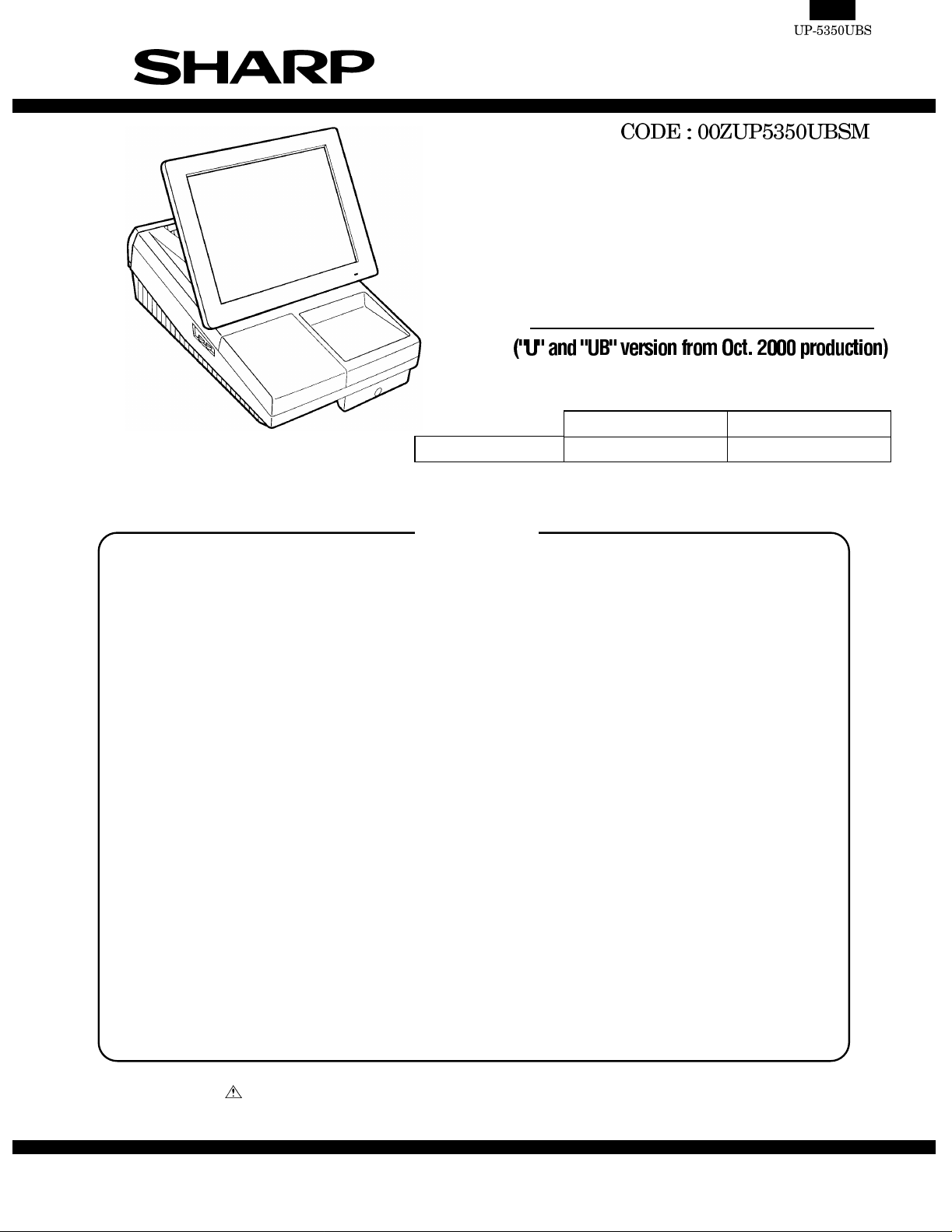
SERVICE MANUAL
POS TERMINAL
MODEL UP-5350
"U" Version "UB" Version
Color of Cabinet parts Gray 282 (light gray) Gray 35 (dark gray)
CONTENTS
■INTRODUCTION
Explanation of modifications
CHAPTER 1. SPECIFICATIONS..................................................................1 - 1
CHAPTER 2. OPTIONS................................................................................2 - 1
CHAPTER 3. SERVICE P RE CA UT ION........................................................3 - 1
CHAPTER 4. UP-535 0 D IAGNOSTICS SPECIFIC ATIONS.........................4 - 1
CHAPTER 5. CIRCUIT DE SC RIPTION........................................................5 - 1
CHAPTER 6. BIOS SETU P UTILITY............................................................6 - 1
CHAPTER 7. ABOUT UTILITY SOFTWARE AND OTHER S.......................7 - 1
CHAPTER 8. CIRCUIT DIA GR AM................................................................8 - 1
CHAPTER 9. PWB LAYOU T.........................................................................9 - 1
PARTS GUIDE
Parts marked with " " are important for maintaining the safety of the set. Be sure to replace these parts with specified
ones for maintaining the safety and performance of the set.
This document has been published to be used
SHARP CORPORATION
for after sales service only.
The contents are subject to chang e w ithout notice.
Page 2

- - - - - - - - - - - - - - - - - - - - - - - - - - - - - - - - - - - - - - - - - - - - - - - - - - - - - - - - - - - - - - - - - - - - - - - - - - - - - - - - - -
-->
BATTERY DISPOSAL
Contains Nickel Metal Hydride Battery. Must be Disposed of Properly.
Contact Local Environmental Officials for Disposal Instructions.
Page 3

■INTRODUCTION
Explanation of modifications
Changes in association with production discontinuance of NeoMagic Graphics Controller
1. APPLICABLE MODELS
MODEL NAME VERSION:CABINET COLOR PRODUCTION PERIOD
UP-5350 U : Gray282 (Light gray) From Oct. 2000
UP-5350 UB : Gray3.5 (Dark gray) New products (1st lot produced in Oct.)
2. OUTLINE
In association with production di scontinuance of NeoMag ic Grap hi cs Controllers,
Silicon Motion Inc. Graphics Controllers will be incorporated.
OLD NEW
PARTS CODE
SOURCE MAKER NeoMagic Silicon Motion Inc
Along with this change, a new function is also add ed so th at th e sta nd ard intern al FDD may become detachable.
For this new function, refer to item 3-4 ).
3. DESCRIPTIONS OF CHANGE
As a result of the Graphics Controller change, those changes described in items 1) - 5) will also be im pl emented.
1) VGA PWB UNIT change
As a result of the Graphics Controller change, the VGA PWB UNIT will
also be changed.
PARTS NAME OLD NEW
VGA PWB UNIT
2) MAIN PWB UNIT change
In parallel with the VGA PWB unit change, the Main PWB unit will also
be changed as follows:
PARTS NAME OLD NEW
MAIN PWB UNIT
• IRQ5 will be assign ed to the new Graphics Controller,
CHIPSET signal (PIRQ5) and No. 77 pin of VGA PWB UNIT connector (CN11) will be conn ecte d.
3) BIOS ROM Change
Since the BIOS PROGRAM must be updated from Version 1.0A to
Version 1 .0B to sup port the new Grap hics Cont roll er, the BI OS MASTER ROM will be change d a s fol lo ws:
PARTS NAME OLD NEW
BIOS MASTER
ROM
You can check the BIOS version in the following system start up
screen, which is displayed when unit is powered on.
(Version 1.0A) (Version 1.0B)
Old BIOS Version 1.0A
Phoenix NoteBIOS
Copyright 1985-1997 Phoenix Technologies Ltd, All Rights Reserved.
SHARP POS Terminal Firmware Version 1.0A
0000640K System RAM Passed
0031744K Extended RAM Passed
0512K Cache SRAM Passed
Fixed Disk 0 : Identified
4.0.0
New BIOS Version 1.0B
Phoenix NoteBIOS
Copyright 1985-1997 Phoenix Technologies Ltd, All Rights Reserved.
SHARP POS Terminal Firmware Version 1.0B
0000640K System RAM Passed
0031744K Extended RAM Passed
0512K Cache SRAM Passed
Fixed Disk 0 : Identified
4.0.1
4) The SYSTEM SWITCH-1, will be enhanced.
The new BIOS al lows the standar d internal FDD to become detatchable, "FDD: Exist/Not Exist" will become selectable with SYSTEM
SWITCH: DSW-1.
SYSTEM SWITCH:DSW-1
Function
FDD Exist Not exist
To detach the FDD drive, turn ON this SWITCH.
*Important:The new BIOS may only be used on units using the Silicon
Motion video controller (Since Oct. production)
OFF
(value=1)
ON
(value=0)
Page 4

5) Software
A new Display driver will be released to support the Graphics Controller.
Windows 98 Second Edition
OLD NEW
FILE NAME DESCRIPTION FILE NAME DESCRIPTION
NMGC5VD2.VxD VGA Virtual Device Driver SMVD D.VxD VG A Virtual Device Driver
NMGC5VDD.VxD VGA Virtual Device Driver SMDRV.DRV VGA Device Driver
NMGC5.DRV VGA Device Driver SMI.INF VGA Driver information file
NMGC5VPM.DRV VGA Device Driver SMDD32.DLL VGA Driver library
NMGC5.INF VGA Driver information file SMI.CAT VGA Driver catalog file
NEOMAGIC.HLP VGA Driver help file NEOMAGIC.DLL VGA Driver library
NMGC5_16.DLL VGA Driver library NMGC5_32.DLL VGA Driver library
NMGCDD5.DLL VGA Driver library TSB.DLL VGA Driver library
Windows NT Workstation 4.0
OLD NEW
FILE NAME DESCRIPTION FILE NAME DESCRIPTION
NEO20XX.SYS VGA Device Driver SMIMINI.SYS VGA Device Driver
NEOMAFIC.INF VGA Driver information file SMISETUP.INF VGA Driver information file
NEOMAGIC.HLP VGA Driver help file SMIDISP.DLL VGA Driver library
NEO20XX.DLL VGA Driver library FRAMEBUF.DLL VGA Driver library
NEOMAGIC.DLL VGA Driver library TSB.DLL VGA Driver library
4. COMPATIBILITY
1) Compatibility between new and old parts
The following parts must be used on ly in the fo llow in g co mbina t ions a s follo ws. N ew and Old parts can not to coexist in the sam e unit.
ITEM OLD NEW Remarks
VGA PWB UNIT
MAIN PWB UNIT
(BIOS Version ) Version 1.0A Version 1.0B Refer to item 3-3).
(SYSTEM SWITCH-1 function) Don’t care FDD:Exist / Not Exist Refer to item 3-4)
Display driver OLD NEW Refer to item 3-5)
IRQ restriction IRQ5 is availab le. IRQ 5 is use d b y System Refer to item 4-2)
When you service the units in the field, take special care not to install the combination of an old Main PWB and a new VGA PWB or a new Main PWB
and an old VGA PWB.
Please modify Main PWB’s in the following methods:
To modify Main PWB’s from old to new,
please refer to item 5-1) please refer to item 5-1) How to modify old Main PWB’s to new Main PWB’s.
With this modification implemented, old Main PWB’s function as new Main PWB’s.
To modify Main PWB’s from new to old,
please refer to item 5-2) How to modify new Main PWB’s to old Main PWB’s
With this modification implemented, new Main PWB’s function as old Main PWB’s.
Important: The old VGA PWB’s cannot be modified to the new VGA PWB’s, or vice ve rsa.
Refer to items 2 and 3-1).
Refer to item 3-2).
Page 5
2) IRQ signal compatibility
The old Graphics Controller does not use an IRQ, while the new
Graphics Controller uses IRQ5.
To avoid IRQ collisions, Please assign IRQ’s other than IRQ5 to the
other devices.
The following chart shows IRQ’s available to optional devices.
IRQ’s available to optional
devices.
IRQ7 LPT1
IRQ10 COM4
IRQ11 COM3
IRQ12 Ethernet/SCSI
Recommended devices for
UP-5350
5. HOW TO MODIFY MAIN PWB’s
1) How to modify old Main PWB’s to new MAIN
PWB’s
A) Connect a jumper w ir e .
Connect the No. 77 pin of VGA Connector (CN11) on Main PWB side
A to the solder pad (PAD2 in JR100) supplying IRQ5 on Main PWB
side B by soldering a jumper wire. (For more information, refer to the
PWB layout.)
B) Change a capaci tor.
Change the capacitance of the Capacitor C536 on the Main PWB B
side from 0.1
0.1
F : VCKYTV1HF104Z -> 1000Pf VCKYTV1HB102K
C) Update the BIOS version.
Rewrite the BIOS to update the version to 1.0B to support the new
Graphics Controller.
To rewrit e t he B IO S p rog r am, pl ea se ref e r t o p ag es 2-6 "W r iti ng BI OS
ROM Program".
F to 1000 pF.
2) How to modify new Main PWB’s to old Main
PWB’s
A) Modify BIOS program
Rewrite the BIOS to modify the version to 1.0A to support the old
Graphics Controller.
There is no need to change the capacitor C536 to 0.1
To rewrite the BIOS program, refer to pages 2-6 "Writing BIOS ROM
Program".
F.
Page 6
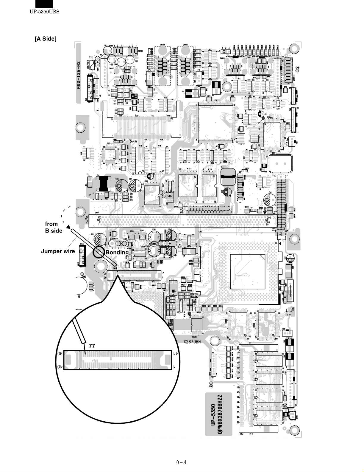
3) PWB LAYOUT
Page 7

Page 8

12345678
(5/21)
D
VCC3
VCC2R5
1 3
JP501
FB560
2
BFD3580R2F
VCC3_GC
VCC5
A
2 1
IC34F
4069
13 12
10
IC34E
4069
11
IC34D
4069
9 8
IC34C
4069
5 6
14PIN --- VCC3
3
PCICLK2
33
R544
1
R14
10k
23
GND4GND11GND17GND
14
VCC5
PERR#
STOP#
RSTDRV#
VCC3_GC
PERR#
RSTDRV#
C546
120p
2
MK1492-04
R208
VCON
RXD7
B
22k
RXD7
PCICLK3
33
R545
C547
120p
2
1
FS32K
OSC32K
47
R1147R13
C20
27p
IC34B
4069
3 4
IC34A
VCC3
VR2
20k VR
BLON
PIRQ5
+12V
VR2-2
VR1
R580
20k VR
22.1kF
X4
32.768KHz
C18
R209
1 2
18p
8.2k
Add
R207
4069
2.32kF
R9 10M
R12 470k
C19
15p
C
FS14M
FSCLK
CPUCLK
CLK_L2
R527
OSC14M
R18 33
R17 33
R15 33
R19 33
5
28
8
13
HOST210HOST312HOST4
F1(PEN)
EHOST1
14.3(OE)
XI2XO
IC39
R22
10M
C28
22p
1
1
1
2
B
F
FB133
BLM21
1
VCC3
C/BE#0
C/BE#2
AD30
AD28
AD26
AD24
SDCLK6SDATA7PCISTP#16CPUS#15VDD1VDD20VDD26VDD_HOST1,29VDD_HOST3,4
3
0
R21
R20
1M
X5
MA-406
14.3181MHz
C27
22p
2
C221
1000p
2
C224
0.1u
2
2
C225
10u
B
F
FB132
1
VCC_CPIO
VCC5
AD22
AD20
AD18
AD16
AD14
AD12
33
1
1
1
10k
R210
1
1
C25
C523
18
HOST5,7
BLM21
AD10
PCICLK
33
R16
C23
10p
10p
HOST6,8(DS)
1000p
0.1u
120p
2
1
27
25
24
22
21
PCI(FS)
PCIF(LE)
PCI(SEL1)
PCI(CSSS)
48M/14M(SEL0)
TRDY#
FRAME#
BR36
10kX4
4
3
2
1
AD4
AD2
AD0
OSC14M
FRAME#
TRDY#
STOP#
10p
2
2
C24
2
C26
10p
19
R211 10k
2
C223
2
C220
5
6
7
8
AD8
AD6
4) CIRCUIT DIAGRAM
BR49
10kX4
4
VCC5
5
6
7
8
C/BE#
3
C/BE#
2
C/BE#
1
C/BE#
3
2
1
0
C/BE#[0..3]
1-1-5. VGA CONNECTOR
D
414243444546474849505152535455565758596061626364656667686970717273
123456789101112131415161718192021222324252627282930313233343536373839
CN11
VCC5
C/BE#3
C/BE#1
AD31
AD29
AD27
AD25
AD23
AD21
AD19
AD17
AD[0..31]
AD15
VCC5
AD13
AD11
AD5
AD3
AD1
OSC32K
BR38
10kX4
IRDY#
DEVSEL#
PCICLK2
4
3
2
1
IRDY#
DEVSEL#
AD9
AD7
5
6
7
8
C
CPAR
CPAR
SERR#
SERR#
VCC3
FANON
TXD7
FANON
74
7576777879
VR2-1
BGNT#
TXD7
BGNT#
B
BREQ#
BREQ#
+12V
80
40
R541
R540
IC34 : 7PIN --- GND
53489-0809
10k
10k
VCC5
8 7 6 5 4
A
Page 9
12345678
(6/21)
D
C
B
A
CS
C548
X1 2X2
AD0
AD1
AD2
4
5
1,2,3
7
3
3p
X3
R581
4Q7Si9430
EXT
SHDN
32.768kHz
VCC2R5
C31
150u/6.3V OS(SL)
C32
OS(SL)
150u/6.3V
R25
100KF
R24
L3 39uH
1
OUT
3
150KF
12
D1
5,6
7,8
SFPB72
2
FB
GND
MAX1651
8
C549
2p
TP2
12
23
22
16
GND
GND
SQW
EXTRAM
MOT
INT#
RST#
R/W#
CS#
BQ3285ESS
1
19
18DS 17
15AS 14
13
2 1
3
RTC
VCC2
(VOUT1=1.9V)
R534
0.010
1/2W(RL3720W)
D501
SFPB54
L501
10uH
RCH-108
28
27
TG1
FLTCPL
RUN/SS1
SENSE+
IC506
1
2
C526
1000p
C525
180p
Q501B
10u/6.3V
(GRM225)
FDS8963A
Q501A
FDS8963A
C537
0.1u
26
25
SW1
BOOST1
SENSE-
VOSENSE1
3
4
R528
49.9kF
10
R535
23
24
VIN
BG1
FREQSET
STBYMD
5
6
VCC5
(VIN=5V)
C542
C543
220uF/4V OS(SP)
150uF/6.3V OS(SP)
C551
C552
10u/6.3V
(GRM225)
C539
0.1u
C540
4.7u/16V
GRM230
D503
RB501V-40
D504
RB501V-40
C541
1u
21
22
20
19
BG2
PGND
INTVCC
EXTVCC
FCB
ITH1
SGND
3.3VOUT
7
8
9
10
TP504
C530
1000p
C531
33p
VCC3
(VOUT2=3.3V)
R536
0.010
D502
SFPB54
Q502B
FDS8963A
Q502A
FDS8963A
C544
0.1u
18
BOOST2
ITH2
11
C533
TP
C532
33p
1/2W(RL3720W)
L502
10uH
RCH-108
17
16
15
TG2
SW2
RUN/SS2
VCC5
VOSENSE2
SENSE2-
SENSE+
LTC1628CG
12
13
14
VRAM
C535
1000p
1000p
2 1
C534
R533
180p
63.4kF
C550
22u/10V
GRM235
C14
100u/10V OS(SA)
VCC5
C160
0.1u
R23
0.22F
5
6
V+
REF
IC41
4
C35
0.1u
C242
1u
TP1
R166
10k
RCL#
24
21
20
BC
VCC
RCL#
AD3
AD4
AD5
AD6
AD7
IC27
6
7
8
9
10
11
1-1-6. RTC
36kF
C524
R529
0.1u
PWRGOOD
15k
R530
C529
0.01u
C528
0.01u
D
15k
20kF
C536
R531
C
0.1u
R532
SD7
SD6
SD5
SD4
SD3
SD2
SD1
SD0
VCC5
R165
New
Old
1000pF
SD[0..7]
0.01µF
B
10k
RTCAS
RTCRD#
RTCWR#
IRQ8#
RSTDRV#
IRQ8#
RTCAS
RTCRD#
RTCWR#
RSTDRV#
8 7 6 5 4
A
Page 10

CHAPTER 1. SPECIFICATIONS
1. APPEARANCE
Brightness
control
Contrast control
Power switch
Operator display
(touch panel)
Power indicator
Money checking
space
Floppy disk drive
3-2. KEYBOARD
TOUCH PANEL
ITEM SPECIFICATIONS NOTE
Type Touch key (Analog touch panel)
Number of
key positions
Control Mouse emulation
4096 (W) x 4096 (H) positio ns
POS KEY PAD
Option (UP-C30PK)
ITEM SPECIFICATION NOTE
Type POS rising ke ybo ard
Number of
keys
Key layout
Standard 27 keys
Numeric keys : 11 keys ( 1 to 9,0 an d 0 0)
Capped keys : 16 keys (Key labels are local ly
purchased.)
Maximum 30 keys (6x5 matrix)
(Changing key layout by using
ER-11KT7/12KT7/22KT7)
789
AC cord
AC CORD
Plug your POS terminal into a wall outlet before using.
POWER SWITCH
Set the power switch to the ON ( I ) position after plugging your POS
terminal.
2. RATING
ITEM SPECIFICATIONS
External dimensions 11.8 (W) x 16.3 (D) x 13.3 (H) in. approximately
(298.5 (W) x 415 (D) x 337 (H) mm )
Weight Approximately 15.5lb. (7.0 kg)
Power source 100 - 120V AC
Power consumption Operating : 74W
Working temperature
and humidity
32 to 104 °F (0 to 40°C)
10%, 60 Hz
3. HARDWARE
3-1. DISPLAY
ITEM SPECIFICATION NOTE
Type DSTN color LCD with back light High color(16bit)
display
Screen size 12.1" full screen
Dot format 800(W) x 3(RGB) x 600 (H) dots
Dot size 0.0825 x RGB(W) x 0.28 25 (H) m m
Control SVGA With 4MB
video RAM
456
123
000
3-3. PC SYSTEM
ITEM SPECIFICATIONS NOTE
CPU MMX Pentium
Chip set FireStar Plus:
Graphic controller VGAC:
Main memory
(for executing MS-DOS,
Application software)
Video RAM 4 Mbytes VGAC Embedded
BIOS ROM 512 Kbytes Flash ROM
Keyboard controller M38802M270
Super I/O M5113 A2
POS system controller PSC2 : LZ9AM22
processor
82C700U3.2
SM712GM04
Standard : 32
Mbytes
Max. : 96 Mbytes adding S.O.DIMM
266MHz
EDO type
SGRAM
Page 11
- - - - - - - - - - - - - - - - - - - - - - - - - - - - - - - - - - - - - - - - - - - - - - - - - - - - - - - - - - - - - - - - - - - - - - - - - - - - - - - - - -
-->
3-4. SERIAL PORT
D-SUB 9-pin connector COM1 and COM2 are eq ui pped.
In order to supply +5V power, CI signal and +5V power supply of
COM1 and COM2 can be switched.
2 channels of RJ45 Connector COM port are equipped.
COM3 and COM4 or original I/O address (COM5 and COM6) can be
selected as the 2 channels of RJ45 COM port.
COM1 & COM2: D-sub 9 pin
Pin No. Signal Function I/O
1 CD Data Carrier Detect I
2 RD Receive Data I
3 SD Send Data O
4 ER Data Terminal Ready O
5 SG Signal Ground —
6 DR Data set Ready I
7 RS Request to Send O
8 CS Clear to Send I
9 CI/+5V Ring Indicate / +5V I/–
COM3 or COM5: Modular jack RJ45 8 pin
Pin No. Signal Function I/O
1 RS Request to Send O
2 ER Data terminal Ready I
3 SD Send Data O
4 SG/(+5V) Signal Ground/(+5V) —
5 SG Signal Ground —
6 RD Receive Data I
7 DR Data set Ready I
8 CS Clear to Send I
COM4 or COM6: Modular jack RJ45 8 pin
Pin No. Signal Function I/O
1 RS Request to Send O
2 ER Data terminal Ready I
3 SD Send Data O
4 SG Signal Ground —
5 SG Signal Ground —
6 RD Receive Data I
7 DR Data set Ready I
8 CS Clear to Send I
3-5. EXPANSION SLOT
ISA PC board can built in UP-5350 up to two.
5V PCI board can built in UP -5 350 instead of an ISA PC bo ard .
This has to satisfy the power consum pti on .
3-6. SHUTDOWN SWITCH
The shutdown switch is used when the OS or applica tion programs
are straying and the system can not return to the normal state.
You must not use this sh utdown s witch whe n the UP- 5350 is r unning
normall y. Use th is swit ch only wh en the mai n power sour ce is n ot cut
off even if the main unit power switch is set to OFF position. The
UP-5350 is turned OFF and the hardware is reset by turning the main
power switch OFF and th en pressing the shutdown sw itch .
12345678
Shut down switch
[OUT LINE]
The shutdown switch is a si ng le shu t type . (Normally OFF position)
Push ON: This position is used to reset the stand-by mode for
power supply unit during softw are hang ups.
Release OFF: Usually the shutdown switch needs to be set to this
position when the UP-5350 is operating.
[OPERATING METHOD]
The shutdown switch is a push switch. If it is pushed to ON, the
UP-5350 stops supplying the power when the power switch is set into
stand-by mode.
NOTE:The shutdown operation will be ignored when the power switch
is set to power-on position.
ITEM SPECIFICATION NOTE
Type ISA bus & PCI bus
Power
consumption
ISA board size Half size PC board ER-A8R S, etc.
5V PCI board size Short size PC board (Local
Quantity 2 slots 2 ISA or ISA + PCI
+5V max. 1.0A
+12V max. 0.05A
procurement item)
Page 12
3-7. SYSTEM SWITCH
The system switches are used to preset various system configurations.
[OUT LINE]
The system switches consists of DIP switche s.
[DIP SWITCH]
12345678
System switch
The PSC2 simply reads the switched signals from the DIP switch as
hardware. The meaning of the switch settings are shown at the right.
ON
1234567 8
ON
OFF
: Default setting
DSW-8
Function
Serial3 & 4
decode mode
OFF
(value=1)
COM3 &
COM4
DSW-7
Function
COM3 &
COM4 IRQ
assign
(Serial 3 & 4)
OFF
(value=1)
COM3=
IRQ11
COM4=
IRQ10
DSW-6
Function
CMOS
Initialize
OFF
(value=1)
Not Initialize
DSW-5 : Reserved (OFF)
DSW-4 : Reserved (OFF)
DSW-3
Function
Boot Drive
OFF
(value=1)
Drive A:
DSW-2 : Reserved (OFF)
DSW-1
Function
Floppy Disk
Drive
OFF
(value=1)
Exit
ON (value=0)
COM5 &
COM6
ON (value=0)
COM3=
IRQ4
COM4=
IRQ3
ON (value=0)
Initialize
ON (value=0)
Drive C:
ON (value=0)
Not exit
Note : On the UP-5350, DSW-1, -2, -4, and -5 are ig no red .
3-8. POWER SWITCH
Power switch :
Page 13
[OUT LINE]
The power switch has the positions ON and OFF (Stand-by)
ON position: Usually the power switch needs to be set to this posi-
tion when the POS-terminal is operated .
OFF position: This position can be used to for the stand-by mode.
When the power switch is set to this position, the
power supply stops automatically. But if the software
program co ntrols the power supply t o hold, ev en if the
power switch is set into this position, the power supply
will stay on until the software program allows a power
supply to turn OFF.
[OPERATING METHOD]
The power switch is a see-saw switch, and it can be tipped toward the
ON or OFF position.
4. SOFTWARE
ITEM SPECIFICATION NOTE
OS provision The OS may be pre-installed.
Available OS Windows 98 Second Edi tio n
Windows NT Work station 4 . 0
Device drivers POS drivers POS device driver Provided from SHARP
Touch panel driver
VGA device driver
Additional device driver
BIOS Written to the Flash ROM on the
Main PWB.
Utility software Touch panel calibration utility program Provided from SHARP
Double t a p setup u t il ity progra m
POS print e r utility pro gram
Application software
Page 14

CHAPTER 2. OPTIONS
1. SYSTEM CONFIGURATION
Additional DRAM
Memory
<Local item>
Magnetic
Card Reader
<Option>
UP-E12MR2
Customer Display
<Option>
UP-I20DP
HDD Unit
<Local item>
PC Keyboard
<Local item>
Drawer
<Option>
ER-03DW/04W
Host
UP-5350
max.2
Incorporated in Main Unit
(Ethernet)
(RS-232)
RS232 Board
<Option>
ER-A8RS
Built-in printer
<Option>
UP-T80BP
In-line Communication Connection
Sub
UP-5350
RS-232 Communication Connection
max.6
Remote Printer
<Local item>
Local Printer
<Option> ER-01PU
<Local item>
Hand Scanner
<Option>
ER-A6HS1
PC server
<Local item>
Kitchen video monitor
<supplied on site>
CAT/EFT
<Local item>
Scale
<Local item>
Customer
Poll Display
<Option>
UP-P20DP
2. OPTIONS
No. NAME MODEL NAME DESCRRIPTION
1 Customer display UP-I20DP 2 line 20 digits dot display
2 Customer pole display UP-P20DP 2 line 20 digits dot display
3 MCR (Magnetic Card Reader) UP-E12MR2 for ISO 1 & 2 stripe card
Remote drawer ER-03DW 7B/5C
4
5 Receip t/Jou rnal printer ER-01PU 2 station (R/J) the rm al pri nte r 45mm width
6 Built-in printer UP-T80BP 1 station thermal printer 80mm width
RS232 & CENTRO I/F board ER-A8RS RS232 9 pins connector:2 ports
7
8 Han d sca nn er ER-A6HS1 for reading bar co de
9 Key pad UP-C30PK Std. 27 keys, Max. 30 keys
Key kit (Used for key pad : UP-C30PK) ER-11KT7 1 x 1 key top kit
10
ER-04DW 5B/5C
Centronics 25 pins connector : 1 port
ER-12KT7 1 x 2 key top kit
ER-22KT7 2 x 2 key top kit
Coin dispenser
<supplied on site>
Page 15

- - - - - - - - - - - - - - - - - - - - - - - - - - - - - - - - - - - - - - - - - - - - - - - - - - - - - - - - - - - - - - - - - - - - - - - - - - - - - - - - - -
-->
3. LOCALLY SUPPLIED OPTIONS
No. NAME DESCRIPTION NOTE
1 S.O.DIMM 144pin Small Outline DIMM Max. 64Mbytes *1
2 Hard disk drive 2.5 inch type *2
3 Ethernet Ethernet adapter *3
4 PC keyboard PS/2 type PC keyboard
5 Application softw are
6 Addition al de vice dri vers
*1 Extension RAM module
[Device] 144pin Small Outline DIMM (8Mbytes/16Mbytes/32Mby-
tes/64Mbytes)
[Outline] UP-5350 has a socket as Small Outline DIMM.
The following S.O.DIMM memory specification must be
adhered to.
[Specification]
144pin S.O.DIMM
8 Mbytes 16 Mbytes 32 M byte s 64 Mbytes
Type EDO type
Access time 60 nsec.(or less)
Power 3.3V
Refresh cycle 1024/16 msec 2048/32 msec. 4096/64 msec. 4096/64 msec.
Refresh type CBR
Power consumption 700 mA (or less)
Other 4 chips x 16Mbits
(1 Mwords x 16 bits)
8 chips x 16Mbits
(2 Mwords x 8 bits)
4 chips x 64Mbits
(4 Mwords x 16 bits)
8 chips x 64Mbits
(8 Mwords x 8 bits)
*2 Hard disk drive
[Device] 2.5 inch type Hard disk drive
[Outline] It is necessary to satisfy with 2.5 inch Hard disk drive
specification as follows.
[Specification]
2.5 inch Hard disk drive
Type 1 Type 2
Maker Fujitsu Toshiba
Model MHD2021AT MK4313MAT
Capacity 2167 Mbytes 4327 Mbytes
Interface ATA-4 ATA-4
*3 Ethernet
[Device] Ethernet adapter
[Outline] It is necessary to satisfy the Ethernet adapter specifica-
tion as follows.
[Specification]
Ethernet adapter
Type 1 Type 2
Maker 3 Com 3Com
Model EtheLink III ISA EtheLink III XL
Speed 10 Mbps 10 Mbps, 100 Mbps
Interface 16-Bit ISA 5V 32-Bit PCI
Page 16

4. SERVI C E OP TIO N S
No NAME PARTS CODE PRICE DESCRIPTION
1 Connector cable for Dongle (LPT-1)
BL Relay line from Terminal to Dongle
5. SERVICE TOOLS
No. NAME PARTS CODE PRICE DESCRIPTION
1 Service tool kit
2 Printer con ne c tor signal loop back connector
3 MCR test card
4 RS232 loop back connector
5 BI OS loadin g board
6 RS232 mo du la r jack loop back connector
7 BIOS MASTER ROM
8 TOUCH PEN
CW ISA checker
ISA relay board
BR for ER-A8RS CENTRONICS connector
BE for UP-E12MR2
BC for RS232 connector
CS for overwriting BIOS
AZ for RJ45 connector
— EP-ROM for overwriting BIOS
AG
5-1. SERVICE TOOL KIT: DKIT-8656BHZZ
1) ISA CHECKER
Used to repair or check the operation of th e o ption al I/F.
• Externa l view
• Plai n view
ISA bus connectors:
Used to connect with the I/F PWB of ER-A8RS etc.
Test pins: Used to check the ISA bus signal.
LED circuit: Not used currently.
RAM1A
Connected to the UP-5350 ISA bus connectors.
Page 17

• Connection diagram
• Connection diagram
ER-A8RS
UP-5350
ISA bus connector
ISA checker
2) ISA RELAY BOARD
Connected to the ISA checker for installation of the optional I/F horizontally and for repairing and checking the opera tio n .
• Externa l view
ER-A8RS solder side
ISA relay board
ISA PWB
ER-A8RS parts side
ISA checker
• Plai n view
ISA bus connector:
Used to check the ER-A8RS parts side.
ISA bus connector:
Used to check the ER-A8RS solder side.
Connected to the ISA bus connector of ISA checker.
5-2. PRINTER CONNECTOR SIGNAL LOOP CHECK
CABLE: UKOG-6717RCZZ
Connected to the centronics connector (25 pin) of the ER-A8RS, and
is used to check loop signals wh en executing diagnostics.
• Externa l view
Page 18
• Plan view and connection diagram
150±8
Signal name Pin No.
1STROBE2DB0
3DB1
4DB2
5DB3
6DB4
7DB5
8DB6
9DB7
10ACK11BUSY
12PE
13SLCT
14AUTOFD15ERROR16INIT17SLCTIN-
18~25PE
• Connection diagram
Signal namePin No.
1 STROBE2 DB0
3 DB1
4 DB2
5 DB3
6 DB4
7 DB5
8 DB6
9 DB7
10 ACK11 BUSY
12 PE
13 SLCT
14 AUTOFD15 ERROR16 INIT17 SLCTIN-
18~25 PE
5-4. RS232 LOOP BACK CONNECTOR:
UKOG-6705RCZZ
Connected to the RS232 connector (D-SUB 9 pin: COM1, COM2,
COM3, COM4 ) of the UP-5350 and ER-A8RS, and used to check loop
signals when executing diagnostics.
• Connection diagram
CD 1pin
RD 2pin
TD 3pin
DTR 4pin
GND 5pin
DSR 6pin
RTS 7pin
CTS 8pin
RI 9pin
5-5. RS232 MODULAR JACK LOOP BACK
CONNECTOR: UKOG-6729BHZZ
Connected to the RS232 connector (RJ45: COM3, COM4, COM5,
COM6) of the UP-5350, and used to check loop signals when executing diagnostics.
• Connection diagram
RTS
1pin
DTR
2pin
TD
3pin
GND
4pin
GND
5pin
RD
6pin
DSR
7pin
CTS
8pin
5-3. MCR TEST CARD: UKOG-6718RCZZ
•
Used when executing the di agnostics of the UP-E12MR2.
• Externa l view
ER-A8RS
5-6. BIOS LOADING BOARD: CKOG-6727BHZZ
The BIOS load ing board: CKOG -6727BHZZ is a t ool to write a B IOS
ROM progra m in the F-RO M on the UP-5 350’s main b oard. Use thi s
PWB in the following cases:
• The F-ROM on the UP-5350’s main board becomes unreadable
and a BIOS ROM program must be written in the F-RO M.
• The BIOS ROM program in the F-ROM is overwritten due to the
BIOS ROM program of the version up, etc.
The BIOS load ing board is connecte d to the Option ROM/RAM dis k
connector (CN5) of the Main PWB.
• Externa l view
Page 19

• Plai n view
Writing BIOS ROM Program
NOTE: Remove all option boards from the ISA slots before writing on
the BIOS ROM.
1. Install the EP-ROM (master ROM): containing a BIOS program on
the BIOS loading board: CKOG-6727RCZZ.
BIOS MASTER ROM
LED1 LED2 LED3 LED4 LED5 LED6 LED7 LED8
SW1
13
Caution: The AC power must be removed prior to installing the
BIOS loading board.
• Connection diagram
Page 20

2. Set SW1 on the BIOS loading b oa rd to the side of pin 3. 3. Open the upper cabin et.
4. Connect the BIOS loading board to the option ROM/RAM connector CN5 on the main PWB , an d then close the cabinet.
LED1 LED2 LED3 LED4 LED5 LED6 LED7 LED8
SW1
5. Writing the BIOS ROM program starts by turning on the power
switch on the right side.
To determi ne the status of t he LED lights on the special serv ice
PWB when a BIOS ROM program is being written, see the table on
the next page.
Writing is complete (automatic completion) when the green LED
SW1
1
3
(LED9) on the BIOS load ing board lights up.
6. After writing is complete, turn off the power switch on the right side
to remove the BIOS loading board, and turn on the power switch
on the left si de ag ai n to c he ck whe the r th e BI OS pr o gra m st art s up
LED9
normally or not.
SW1
1
3
Page 21
LED DISPLAY STATUS
[ : ON (Lighting) — : OFF]
<In normal operation>
LED1
(RED)
————
—————
————
————
—
———
—
——————
——————
—
———
—
————
LED2
(RED)
——— ———
—— — — — Programming: Bank1 D0000 h (64KB)
————— ——
—— —— — — Verifying: Bank1 D0000 h (64KB)
LED3
(RED)
—— — — — Programming: Bank0 E0000 h (64 K B)
—— ———
— ———
— ———
———— — — Verifying: Bank0 E0000 h (64KB)
———— — — Verifying: Bank0 F0000 h (64KB )
— —— — — Verifying: Bank1 E0000 h (64KB)
— —— ——
LED4
(RED)
LED5
(RED)
—— ——
LED6
(RED)
————
— ——
LED7
(RED)
— — — Erasing F-ROM (LED6: RED is blinking)
— — — Start copy programming to F-ROM from EP-ROM
———
———
LED8
(RED)
— — Start verifying the program in the F-ROM
— — Verifying: Bank0 C0000 h (64KB)
LED9
(GREEN)
— Start of COPY FUNCTION
Start initializing
Programming: Bank0 C 0000 h (64KB)
Programming: Bank0 D 0000 h (64KB)
Programming: Bank0 F 0 000 h (64KB)
Programming: Bank1 C 0000 h (64KB)
Programming: Bank1 E0000 h (64KB)
Programming: Bank1 F 0 000 h (64KB)
Verifying: Bank0 D0000 h (64 K B)
Verifying: Bank1 C0000 h (64 KB )
Verifying: Bank1 F0000 h (6 4KB )
Setting protection for F-ROM
END of complete COPY FUNCTION
FUNCTION
<Erase ERROR in F-ROM>
LED1
(RED)
—
——
<Programming ERROR in F-ROM>
LED1
(RED)
—
<Verifying ERROR in F-ROM>
LED1
(RED)
—
LED2
(RED)
———— — —
LED2
(RED)
——— — — Device not ready
LED2
(RED)
——— — —
LED3
(RED)
——— — — VPP error
——— — —
LED3
(RED)
—— — —
—— — — Command sequen ce error
LED3
(RED)
—— — — Can not release the protection
LED4
(RED)
—— — —
LED4
(RED)
LED4
(RED)
LED5
(RED)
LED5
(RED)
LED5
(RED)
LED6
(RED)
LED6
(RED)
LED6
(RED)
LED7
(RED)
LED7
(RED)
LED7
(RED)
LED8
(RED)
LED8
(RED)
LED8
(RED)
LED9
(GREEN)
LED9
(GREEN)
LED9
(GREEN)
FUNCTION
Device not ready
Command sequence e rror
FUNCTION
VPP error
FUNCTION
Device not ready while releasing the protection
Page 22

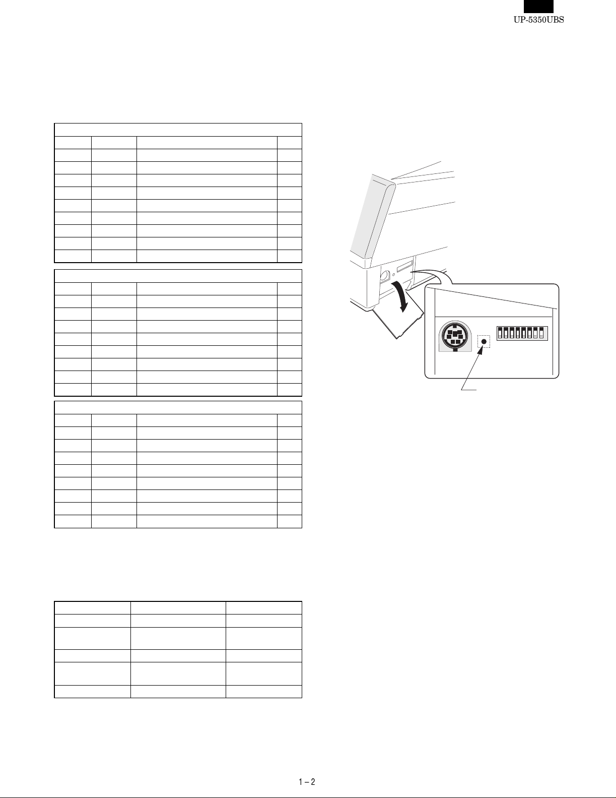
CHAPTER 3. SERVICE PRECAUTION
1. CONDITIONS FOR SOLDERING
CIRCUIT PARTS
To solder the fo ll ow ing pa rt s m anu al ly , fol lo w the co ndi ti on s d esc ri be d
below.
PARTS NAME PARTS CODE LOCATION CONDITIONS FOR SOLDERING
Ceramic oscillator
DIP SWITCH
TOUCH PANEL CONTROL PWB: X1 (8M) 270°C/3sec.
MAIN PWB: X2 (24M)
MAIN PWB: X2 (7.37M)
SWITCH PWB: S2 300°C/3sec.
2. CAUTIONS ON HANDLING CPU AND
POWER FAN
When removing or performing maintenance activities on the CPU and
POWER FAN, be sure to handle them with care, because it may
cause abnormal sounds or deteriorate th eir performance if th ey are
dropped or exposed to a heavy impact.
3. NOTE FOR HANDLING OF TOUCH
PANEL
• The transparency of the touch panel should be vitally important.
Use clean gloves and masks.
• For handling, do not hold the transparent area, and do not hold the
heat seal connector section to assure reliability.
• Do n ot o verl ay to uch panels. The edge ma y damage the surface.
• Do not place heavy things on the touch panel.
• Do not apply a strong shock, and do not drop it.
• When attaching the protection film again, carefully check for dirt. If
there is any dirt, it is transferred.
• To clean dirt on the surface, use a dry, soft cloth or a cloth im-
mersed in ethyl alcohol.
• Check that the housing does not give stress to the touch panel.
• Be care ful no t to to uch the touch panel with tools.
• Th e he at sea l se ctio n is easily disconnected. Be carefu l not to pl ace
stress to the heat seal section wh en installing.
• The touch panel is provided with an air groove to make the external
and the internal air pressure equal to each other. If water or oil is
put around the air groove, it may penetrate inside. Be careful to
keep the air groove away from water and oil.
• Do n ot u se sharp objects when making in pu t entrees.
4. NOTE FOR HANDLING OF LCD
• The LCD elements are made of glass. BE careful not to expose
them to strong mechanical shock, or they may be broken. Use
extreme care not to break them.
• If the LCD element is broken and the liquid leaks, avoid contact with
your mouth or eyes . If th e liq uid co mes in c ontac t with y our s kin or
clothes, immediately clean w ith soap.
• Use the unit under the rated conditions to prevent against damage.
• Be careful not to place water or o the r liquids on the display surface.
• The reflection plat e and the polarizing pl ate are easily scra tched.
BE careful not to touch them with a hard object such as glass,
tweezers etc. Never hit, push, or rub the surface with hard objects.
• When installing the unit, be careful not to apply stress to the LCD
module. If excessive stress is applied, abnormal display or uneven
color may result.
5. CAUTIONS ON HANDLING
CONNECTORS
When connec ti ng or d is c onn ec ti ng the fol l owi ng co nnec to r s, fol l ow th e
procedures below.
1)
PARTS NAME PARTS CODE LOCATION
FFC
CONNECTOR
How to insert FFC
(1) Pull the slider to the unlock position.
LCD RELAY
PWB: CN6
Page 23
- - - - - - - - - - - - - - - - - - - - - - - - - - - - - - - - - - - - - - - - - - - - - - - - - - - - - - - - - - - - - - - - - - - - - - - - - - - - - - - - - -
-->
(2) Open the slider upwards.
(3) Inserting the FFC
Insert the FFC firmly until the FFC hits the bottom of the connector’s insulator.
FFC
FFC FFC FFC
CONNECTOR CONNECTOR CONNECTOR
(4) Close the slider to the lock position
FFC
FFC
6. PS2 Keyboard usable f or UP- 5 35 0
The UP-5350 can be e xtern al ly co nn ected to a keyboard.
The UP-5350’s key BIOS conforms to the PC standard, but this
BIOS’s operation is not compatible for some keyboards.
Some keyboards may cause operation errors due to delicate timing
and conflicts.
It is currently found that the following models of keyboards may malfunction.
When selecting a keyboard to be connected, test the keyboard in
advance to check that it correctly wo rks.
• Japa nese keyboard (106 keys)
Manufactured by IBM: TYPE/MODEL5576-B01 FRUPN66G0507
• English keyboard (101 keys)
Manufactured by NMB Technologies Inc.: Model: RT6651T+
Page 24

CHAPTER 4. UP-5350 DIAGNOSTICS SPECIFICATIONS
CONTENT
1. General ...................................................................................... 4-1
2. System configura tion .................................................................4-1
3. Service diagnostics ...................................................................4-1
3-1. Service diagnostics getting started .................................4-1
3-2. Selection menu ................................................................ 4-2
3-3. RAM Diagnostics ............................................................. 4-2
1) D-RAM Check ......................................................... 4-2
3-4. ROM Diagnostics ............................................................ 4-2
1) BIOS ROM Check ................................................... 4-2
3-5. Real time clock & CMOS RAM Diagnostics .................... 4-2
1) Real time clock Check ............................................4-2
2) CMOS RAM Check ................................................. 4-3
3-6. Touch Panel Diagnostics ................................................ 4-3
1) Controller Diagnostics Test .....................................4-3
2) Touch Key Pad Test ...............................................4-3
3) Linearity Test ........................................................... 4-3
3-7. Key Pad Diagnostics ....................................................... 4-4
1) Key Pad Check ....................................................... 4-4
3-8. Clerk Key Diagnostics ..................................................... 4-4
1) Clerk Key Check ..................................................... 4-4
3-9. Printer Diagnostics .......................................................... 4-4
1) PARALLEL1 Loop Check ....................................... 4-5
2) PARALLEL2 Loop Check ....................................... 4-5
3) PARALLEL3 Loop Check ....................................... 4-6
4) PARALLEL1 Print Check ........................................ 4-6
5) PARALLEL2 Print Check ........................................ 4-6
6) PARALLEL3 Print Check ........................................ 4-7
7) UP-T80BP Test ....................................................... 4-7
3-10. Serial I/O Diagnostics ......................................................4-7
1) COM1 Check .......................................................... 4-8
2) COM2 Check .......................................................... 4-8
3) COM3 Check .......................................................... 4-8
4) COM4 Check .......................................................... 4-8
5) COM5 Check .......................................................... 4-8
6) COM6 Check .......................................................... 4-8
3-11. Liquid Crystal Display Diagnostics .................................. 4-8
1) Liquid Crystal Display Check .................................. 4-9
3-12. Magnetic Card Reader Diagnostics .............................. 4-10
1) Magnetic Card Reader Check .............................. 4-10
3-13. System Switch Diagnostics ........................................... 4-10
1) System Switch ...................................................... 4-10
3-14. Drawer Diagnostics ....................................................... 4-10
1) Drawer 1 Check .................................................... 4-10
2) Drawer 2 Check .................................................... 4-11
3-15. Option Display Diagno stics ........................................... 4-11
3-16. IDE I/F & HARD DISK Diagnostics ............................... 4-11
[READ MODE TEST] .................................................... 4-11
1) Drive Status display .............................................. 4-11
2) Sequential Seek Test ............................................ 4-11
3) Random Seek Test ............................................... 4-12
4) Seek & Read Test ................................................. 4-12
5) Target Sector Read Test ...................................... 4-13
6) HD Dump Test ...................................................... 4-13
■ DIAGNOSTICS PROGRAM: CREATING AN
Before ex e cut i ng t he Di ag no st ic pr o gra m, cr e ate th e MS- DO S s ta r tin g
media and copy the Diagnostics program onto it.
How to create an MS-DOS starting media
1. GENERAL
This diagnostic program is used to check the PWB’s, the process, and
the machine of UP-5350 series in a simplified manner.
This test program is supplied with floppy di sks.
2. SYSTEM CONFIGURATION
The system requires the UP-5350, and a PS2 keyboard for diagnostic
operations.
3. SERVICE DIAGNOSTICS
3-1. SERVICE DIAGNOSTICS GETTING STARTED
Getting started:
Execute "S RV.BA T" by en teri ng the c ommand with th e PS2 keyb oard
as follows:
"A:\>" is the DOS prompt. (Used by the FD : Floppy disk based on the
settings of the system switches.)
7) Error lnformation Display .......................................4-14
8) Controller check Test ............................................4-14
[WRITE MODE TEST] ...................................................4-14
9) Seek&Write/Read-Verify Test ...............................4-14
10) Target Sector Write/Read-Verify Test ...................4-15
11) HD Patch Test (Utility) ...........................................4-15
12) Error Logging Area Clear ......................................4-15
13) Error table display ..................................................4-16
14) Other Supplemental Items .....................................4-16
15) Error Content .........................................................4-16
16) Error Information Storing Area Description ...........4-16
3-17. FDD Diagnostics ............................................................4-16
3-18. FAN & LCD ON/OFF Diagnostics ..................................4-17
1) FAN & LCD ON/OFF Check ..................................4-17
3-19. Power Hold Diagnostics .................................................4-17
1) Power Hold Check .................................................4-17
MS-DOS STARTING MEDIA (FD)
1) Execute the command given below on the PC where the MS-
DOS Ver. 6.22 is running and create an MS-DOS starting media (FD).
MS-DOS (Command) format a: /s
2) Copy the Diagnostics program onto the MS-DOS starting media
(FD).
A:\> SRV
Do not load any device drivers when using this program.
To operate other ap pl ic at io ns af te r perf o rm in g thi s prog r am, re - boot
the machine.
Page 25

- - - - - - - - - - - - - - - - - - - - - - - - - - - - - - - - - - - - - - - - - - - - - - - - - - - - - - - - - - - - - - - - - - - - - - - - - - - - - - - - - -
-->
3-2. SELECTION MENU
The diagnost ics menu is s tarted and t he followin g menu is dis played.
The highlighted cursor is moved by the cursor keys (UP
) of the PS2 keyboard. Move the cursor to the desired item, and
press the Enter key to execute the selected diagnostics program.
When the selected diagnostics program is completed, the display returns to t he menu scr een by pre ssing the E SC key. Se lect "Dia gnostics End" and press the Enter ke y to te rm inate the diagnostics.
SHARP PC-POS System Diagnostic Series III
Diagnostics for Service
RAM Diagnostics
ROM Diagnostics
Real time clock & CMOS RAM Diagnostics
T ouch Panel Diagnostics
Key Pad Diagnostics
Clerk Key Diagnostics
Printer Diagnostics
Serial I/O Diagnostics
LCD (Liquid Crystal Display) Diagnostics
MCR (Magnetic Card Reader) Diagnostics
System Switch Diagnostics
Drawer Diagnostics
Option Display Diagnostics
IDE I/F & Controller Diagnostics
FDD Diagnostics
FAN&LCD ON/OFF Diag nos tics
Power Hold Diagnostics
Diagnostics End
and DOWN
Version 1.00B
are not displayed.)
Terminating method
After completion of the test, press Esc key to terminate and return
to the service diagnostics menu .
3-4. ROM DIAGNOSTICS
The BIOS ROM, is tested.
1) BIOS ROM CHECK
Checking content
The BIOS ROM version is displayed.
Display
BIOS ROM Check
Version - ROM : SHPUP****
The version is displayed.
Terminating method
After the test result is displayed, press Esc key to terminate and
return to the service diagnostics menu.
3-3. RAM DIAGNOSTICS
This progr am is used to test t he standard memory and t he extensi on
memory.
1) D-RAM CHECK
Checking content
All memory areas are checked in blocks of 64KB. The checking
procedures are as follows:
i. Test data 5555H is written to all the test areas.
ii. Test data and read data are compared by each word, If it is
O.K., test data AAAAH is written to the test area.
iii. Test data and read data are compared by each word, If it is
O.K., test data 5555H is written to the test area .
iv. Test data 0000 H is written to all the test areas.
v. Test data and read data are compared by each word, If it is
O.K., test data FFFFH is written to the test area.
vi. Test data and read data are compared by each word, If it is
O.K., test data 0000H is written to the test area .
When an error occurs during the test, the error address and data
are displayed and the test is stop pe d.
For the extended memory test, the value set in the setup of read
and test and is made to the area in incre m en ts of 64KB.
Display
D-RAM Check
Main memory size : 640KB PASS !!(or ERROR !!)
Extended memory size : xxxxKB PASS !!(or ERROR !!)
Error Address xxxxxxH Write Data xxxxH Read Data xxxxH
3-5. REA L TIME C L OCK & CMOS RAM DIAG NOSTIC S
RTC and CMOS RAM check is performed.
The followin g menu is disp layed. The hi ghlighted cur sor is moved by
the cursor keys (UP
cursor to the desired item, and then press the Enter key to execute the
selected diagnostics program. When the selected diagnostics prog ram
is completed. Pressing Esc key again returns to the service diagnostics menu.
Real time clock & CMOS RAM Diagnostics
Real time clock Check
CMOS RAM Check
1) REAL TIME CLOCK CHECK
Checking content
RTC timer function and RTC clock function are tested.
In RTC timer check, the RTC timer is set so that an interrupt is
generated after 2 sec and checked that the interrupt is performed
properly. In RTC clock check, the RTC clock is set to 23:59:58,
31/Dec/1989, and checks that the clock shows 0:0:0, 1/Jan/1990
after 2 sec.
Display
Real time clock Check
RTC Timer Check : PASS !!(or ERROR !!)
RTC Clock Check : PASS !!(or ERROR !!)
and DOWN ) of the PS2 keyboard. Move the
When testi ng the exte nsion me mory siz e, the val ue of the exi sting
memory is displayed. The error address and the error data are
displayed only when an error occurs. (When no errors occur, they
Terminating method
After the test result is displayed, press Esc key to terminate and
return to the RTC and C M OS RAM diagnostics menu.
Page 26

2) CMOS RAM CHECK
Checking content
The read/wri te check is performed for CMOS-RAM wh en setting
up. The checking procedure is as follows:
i. Test address data is saved to the main memory.
ii. Test data 55H is written to the test address.
iii. Te st data and read data are compared , and test data AAH is
written to the test address.
iv. Test data an d re ad data are compared.
v. The saved test data is written to th e test area.
vi. The addre ss is incre m ented until it becomes 3FH.
If POFF interruption is generated during the test, the test is
stopped and the saved data is w ritten to the test area within 50ms.
Display
CMOS-RAM Check
RTC RAM Check : PASS !!(or ERROR !!)
Error Address xxxxxH Write Data xxH Read Data xxH
The error address and t he error bit are di splayed only when an
error occurs. (When no error occu rs, they are not displayed.)
Terminating method
After the test result is displayed, press Esc key to terminate and
return to the RTC and C M OS RAM diagnostics menu.
3-6. TOUCH PANEL DIAGNOSTICS
The touch pane l and its contr oller are chec ked. Communicat ion with
the controller is performed by 8250 built in the gate array PSC2.
The controller diag check, the touch keypad test, and the linearity test
are performed.
The initial display is as follows:
Return code Content
0Ah ROM error
0Bh RAM error
0Ch Panel voltage error
0Dh Reserve
0Eh EPROM write error
0Fh EPROM read error
10h EPROM check sum erro r
Display
Controller Diag Test
Pass!!
ROM Error!!
or
RAM Error!!
PANEL Voltage Error!!
EPROM Write Error!!
EPROM
EPROM SUM Error!!
Error!!
Error!!
Read Error!!
Terminating method
After the test result is displayed, press the Esc key to terminate
and return to the Touch pa nel diagnostics menu.
2) TOUCH KEY PAD TEST
Checking content
The driver function call is used.
ners of the LCD sequentially.
(In the sequence of uppe r right, u pp er left, low er left, low er righ t.)
When the
the screen turns to
is touched by the operator, the buzzer sounds and
.
Display
Touch Key Pad Test
Touch Cursor !!
is displayed at the four cor-
Touch Panel Diagnostics
Controller Diag Test
Touch Key Pad Test
Linearity
1) CONTROLLER DIAGNOSTICS TEST
Checking content
After initializing the controller, the diagnostic command is exe-
cuted. The procedures are as follows:
• One byte of sample data (FFh) is sent and a wait state of 100ms
is made.
• The re set command ( 80h) is sen t and a wait stat e for the end
code (2 bytes: 90h and 00h) fro m the controller is made.
• The di agnostic command ( 2 bytes: 89h, any o ne-byte data) is
executed, and a wait state f or the end code (3 bytes: 90h, return
code, any one-byte data) is made.
• If an error occurs the error display is made with the return cod e.
To exit from the controller diagnostic test, press the Esc key
during the wait state for the end code response.
Terminating method
Touch all four
or press the Esc key to terminate and return to
the Touch panel diagnostics menu.
3) LINEARITY TEST
Checking content
Red lines ar e di spl aye d at bo th si des of th e blu e li ne at th e cent er.
The operator must touch the blue line without touching the red lines
and drag from top to bo ttom.
The touched part of the bl ue line is ch anged to white.
If the red line is touched, an erro r messa ge is issued.
Page 27
Display
About 2cm
Linearity
Test
Complete!
(Error!!)
Displayed after termination.
Red line
Blue line
About 1cm
Red line
Terminating method
Press Esc k ey to t e rmi nat e an d r et urn to t h e Touc h pa ne l d ia gnos -
tics menu.
3-8. CLERK KEY DIAGNOSTICS
(Not used for "U/B" models)
The clerk key input test is performed.
Pressing the Esc key returns to the se rvicem an diagnostics menu.
1) CLERK KEY CHECK
Checking content
Key code inserted to the clerk key switch which is then displayed in
a decimal value.
Display
Clerk Key Check
Clerk Key Code : xx
3-7. KEY PAD DIAGNOSTICS
1) KEY PAD CHECK
The UP-C30PK k ey test is per formed. I n the UP-C30 PK, key s are
detected by matrix scan of KBC (M 38 80 2M 270).
Display
Key Pad Diagnostics
When this is pressed, the buzzer sounds
and the color changes.
ESC
Press ESC key to exit.
Content
When a key is pressed, its color changes and the key catch sound
is made.
The keys to be checked an d th ei r po sitions are as shown below.
ESC
F4
F5
F10 Delete
Back
Space
The clerk code is displayed at XX.
Terminating method.
Press the Esc key to terminate and return to the service diagnos-
tics menu.
3-9. PRINTER DIAGNOSTICS
The parallel interface (standard) and ER-A8RS parallel interface (option) are tested.
Here, the parallel interface on the main body is mentioned as PARALLEL1, and the parallel interface on ER-A8RS as PARALLEL 2/3.
The following menu is displayed.
Printer Diagnostics
Standard Option(ER-A8RS)
PARALLEL 1 Loop Check
PARALLEL 1 Print Check
Option(UP-T80BP)
Print Check ALLEL3 Print Check
The highlighted cursor is moved by the cursor keys (UP
) on the PS2 keyboard. Move the cursor to the desired item and
press the Enter key to execute the selected diagnostics program.
When the selected diagnostics program is completed, the display re-
turns to the menu screen. Pressing the Esc key returns to the service
diagnostics menu.
P ARALLEL2 Loop Check
P ARALLEL3 Loop Check
P ARALLEL2 Print Check
PAR
and DOWN
Tab
9
8
7
L-Shift
6
5
4
L-Ctrl
3
2
1
0
L-Alt
End
Press the ESC key to terminate the test.
Space
Enter
Page 28
1) PARALLEL1 LOOP CHECK
Checking content
A loop check is made for the standard I/O address 378H ~ 37FH.
(PARALLEL1)
In the lo op check, a nor mally-oper ating ER-A8R S is inserted and
the loop c able (U KOG-6717 RCZZ) is c onnecte d between P ARALLEL1 and PAR ALLEL3 ( ER-A8 RS) for testing . Set th e jumper s on
the PWB prior to the test as follows:
Signal name
STROBE-
DB0
DB1
DB2
DB3
DB4
DB5
DB6
DB7
ACKBUSY
PE
SLCT
AUTOFD-
ERROR-
INIT-
SLCTIN-
GND
1
2
3
4
5
6
7
8
9
10
11
12
13
14
15
16
17
18~2
Loop cable (UKOG-6717RCZZ) wiring diagram
J3J8J4J5J6
J7
10
UP-5350 : PARALLEL1 OUTPUT MODE
A8RS : PARALLEL3 INPUT MODE
J9
J10
I
L
H
57
O
J18
Opposite ER-A8RS setting
Jumper pin setting diagram
Display
PARALLEL1 Loop Check
ACK- Signal : PASS !!(or ERROR !!)
BUSY Signal : PASS !!(or ERROR !!)
PE Signal : PASS !!(or ERROR !!)
SLCT Signal : PASS !!(or ERROR !!)
ERROR- Signal : PASS !!(or ERROR !!)
STROBE- Signal : PASS !!(or ERROR !!)
AUTOFD- Signal : PASS !!(or ERROR !!)
INIT- Signal : PASS !!(or ERROR !!)
SLCTIN- Signal : PASS !!(or ERROR !!)
INTERRUPT : IRQ X (or ERROR !!)
DATA Bus : PASS !!(or ERROR !!)
J11
J12
J13
J14
J15
J16
J17
18~2
12
Signal namePin No.
1
STROBE2
3
4
5
6
7
8
9
10
11
12
13
14
AUTOFD-
15
ERROR-
16
INIT-
17
SLCTIN-
DB0
DB1
DB2
DB3
DB4
DB5
DB6
DB7
ACKBUSY
PE
SLCT
GND
Terminating method.
Press the Esc key to terminate and return to the Printer diagnostics
menu.
2) PARALLEL2 LOOP CHECK
Checking content
A loop check is perf orme d for E R-A8RS I/O ad dres s 278H ~ 27 FH
(PARALLEL2).
In the loop check, the loop cable shown in Fig, 3-4 is connected
between PARALLEL2 (ER-A8RS) and PARALLEL1 for testing. Set
the jumpers on the PWB prior to the te st as sh own in Fig. 3-6.
J3J8J4J5J6
Display
PARALLEL2 Loop Check
ACK- Signal : PASS !!(or ERROR !!)
BUSY Signal : PASS !!(or ERROR !!)
PE Signal : PASS !!(or ERROR !!)
SLCT Signal : PASS !!(or ERROR !!)
ERROR- Signal : PASS !!(or ERROR !!)
STROBE- Signal : PASS !!(or ERROR !!)
AUTOFD- Signal : PASS !!(or ERROR !!)
INIT- Signal : PASS !!(or ERROR !!)
SLCTIN- Signal : PASS !!(or ERROR !!)
INTERRUPT : IRQ X (or ERROR !!)
DATA Bus : PASS !!(or ERROR !!)
The inter r uption le v e l is displa y e d at XX.
If no access is allowed to PARALLEL2, the following display is
made.
PARALLEL2 Loop Check
Terminating method.
Press the Esc key to terminate and return to the Printer diagnostics
menu.
J7
10
UP-5350 : PARALLEL1 INPUT MODE
J9
J10
L
H
57
O
Setting of ER-A8RS to be tested
Fig. 3-6 Jumper pin setting
PARALLEL2 Channel Disabled
A8RS : PARALLEL2 OUTPUT MODE
I
12
J18
J11
J12
J13
J14
J15
J16
J17
The inter r uption le v e l is displa y e d at X.
When no ac cess is allo wed to PARALLEL1, the following display is
made.
PARALLEL1 Loop Check
PARALLEL1 Channel Disabled
Page 29
3) PARALLEL3 LOOP CHECK
Checking content
A loop check is performed for ER-A8RS I/O address 3BCH ~
3BEH (PARALLEL3).
In the loop check the ER-A8RS is connected to the extension slot
and the loop cable shown in Fig. 3-4 is connected between PARALLEL3 (ER -A8RS) and PAR ALLEL1 for te sting. Set t he jumpers
on the PWB prior to the test as show n in Fig. 3 -6.
J3J8J4J5J6
Display
J7
10
UP-5350 : PARALLEL1 OUTPUT MODE
A8RS : PARALLEL3 INPUT MODE
J10
J9
I
L
H
57
O
J18
J11
J12
J13
Setting of ER-A8RS to be tested
Fig. 3-6 Jumper pin setting
J14
J15
J16
12
J17
Display
PARALLEL1 Print Check
PARALLEL1 Channel Disabled
"PARALLEL1 Channel Disabled" is displayed only when no access
to PARALLEL1 is allowed.
Terminating method.
Press the Esc key to terminate and return to the Printer diagnostics
menu.
5) PARALLEL2 PRINT CHECK
Checking content
The print check is performed for PARALLEL2 at I/O address 278H
~ 27Fh on the ER-A8RS.
In the print check, set the short pin of the ER-A8RS to be tested as
shown in Fig. 3-9, and connect the D- Sub 25 pin connector to a
printer to allow a print pattern test.
PARALLEL3 Loop Check
ACK- Signal : PASS !!(or ERROR !!)
BUSY Signal : PASS !!(or ERROR !!)
PE Signal : PASS !!(or ERROR !!)
SLCT Signal : PASS !!(or ERROR !!)
ERROR- Signal : PASS !!(or ERROR !!)
STROBE- Signal : PASS !!(or ERROR !!)
AUTOFD- Signal : PASS !!(or ERROR !!)
INIT- Signal : PASS !!(or ERROR !!)
SLCTIN- Signal : PASS !!(or ERROR !!)
INTERRUPT : IRQ X (or ERROR !!)
DATA Bus : PASS !!(or ERROR !!)
The inter r uption le v e l is displa y e d at XX.
If no access is allowed to PARALLEL3, the following display is
made.
PARALLEL3 Loop Check
PARALLEL3 Channel Disabled
Terminating method.
Press the Esc key to terminate and return to the Printer diagnostics
menu.
4) PARALLEL1 Print Check
Checking content
The print check is performed for the standard port PARALLEL1 at
I/O address 378H ~ 37FH. In the print check mode the D-Sub 25
pin connector is connected with a printer to allow a print pattern
test.
The test procedures are as follows:
i. Data of 55H is written to I/O address 378H, and the same
address is read. If the read data is not 55H, "PARALLEL1
Channel Disa bled" is displ ayed and the followi ng check is not
performed.
ii. C harac ters of 20H ~ 7FH (AS CII co de) are pr inte d and the l ine
is changed.
This procedure is repeate d fo r 5 ti m es.
J3J8J4J5J6
J7
10
J10
J9
L
H
57
I
O
J18
J11
J12
J13
J14
J15
J16
12
J17
Fig. 3-9 Jumper pin setting
The test procedures are as follows:
i. Data of 55H is written to I/O address 278H, and the same
address is read. If the read data is not 55H, "PARALLEL2
Channel Disa bled" is displ ayed and the followi ng check is not
performed.
ii. C harac ters of 20H ~ 7FH (AS CII co de) are pr inte d and the l ine
is changed.
This procedure is repeate d fo r 5 ti m es.
Display
PARALLLEL2 Print Check
PARALLEL2 Channel Disabled
"PARALLEL2 Channel Disabled" is displayed only when no access
to PARALLEL2 is allowed.
Terminating method.
Press the Esc key to terminate and return to the Printer diagnostics
menu.
Page 30

6) PARALLEL3 PRINT CHECK
Checking content
The print check is performed for PARALLEL3 at I/O address 3BCH
~ 3BEh on the ER-A8RS.
In the print check, set the short pin of the ER-A8RS to be tested as
shown in Fig. 3-10, and connec t the D-Sub 25 pin c onnector to a
printer to allow a print pattern test.
Testing
The followin g patterns are p rinted and the p aper cut command is
sent by th e specified number of times to the Se rial output of I/O
address 980H to 987H.
J3J8J4J5J6
J7
10
J10
J9
L
H
57
I
12
O
J18
J11
J12
J13
J14
J15
J16
J17
Fig. 3-10 Jumper pin setting
The test procedures are as follows:
i. Data of 55H is written to I/O address 3BCH, and the same
address is read. If the read data is not 55H, "PARALLEL3
Channel Disa bled" is displ ayed and the followi ng check is not
performed.
ii. C harac ters of 20H ~ 7FH (AS CII co de) are pr inte d and the l ine
is changed.
This procedure is repeate d fo r 5 ti m es.
Display
PARALLEL3 Print Check
PARALLEL3 Channel Disabled
"PARALLEL3 Channel Disabled" is displayed only when no access
to PARALLEL3 is allowed.
Terminating method.
Press the Esc key to terminate and return to the Printer diagnostics
menu.
7) UP-T80BP TEST
Display
Print Check
Count ? = 01 (00-99)
Pass Count = XX
Hit ESC Key to Stop
On the above screen the setting appears in the box.
The Count can be set from "01" up to "99". If "00" is set, printing
does not stop until the ESC key is pressed.
YOUR RECEIPT
THANK YOU
Error message
The following error message appears if a communication error
occurs with the UP-T80BP.
Print Check
CD 1pin
RD 2pin
TD 3pin
DTR 4pin
GND 5pin
DSR 6pin
RTS 7pin
CTS 8pin
RI 9pin
RTS
1pin
DTR
2pin
TD
3pin
GND
4pin
GND
5pin
RD
6pin
DSR
7pin
CTS
8pin
********************
UP-T80BP I/F ERROR
Hit ESC Key to Stop
End of testing
The testing is fi nishe d afte r pri nting is made by the s pecif ied num-
ber of times or by pressing the ESC ke y.
3-10. SERIAL I/O DIAGNOSTICS
The serial interface of UP-5350 and the option PWB ER-A8RS is
performed. To test the 9pin D-Sub port, connect the D-Sub loop back
connector (UKOG-6705RCZZ).
To test the RJ45 port, connect the loop back connector (UKOG6729BHZZ).
Loop back connector (UK OG-6705RCZZ) wiring diagra m
Loop back connector (UKOG-6729BHZZ) wiring diagram
The UP-535 0’s 9-pin D-sub port s are used as COM1 and 2. In a ddition, th e UP-5350’s RJ45 ports are use d as COM3 and 4 or CO M5
and 6 accor di ng t o t he set up. O n th e o the r ha nd , E R-A 8RS i s us e d by
selecting either COM1 and 2 or COM3 and 4 according to the setup.
Therefore , when an ER-A8 RS is us ed, yo u must s et COM1 , 2, 5, an d
6 on the UP-5350 side, and set COM3 and 4 on the ER-A8RS side.
Page 31

The following menu is displayed.
The highlighted cursor is moved by the cursor keys (UP
and DOWN
) of the PS2 keyboard. Move the cursor to the desired item, and
press the Enter key to execute the selected diagnostics program.
When the selected diagnostics program is completed, the display re-
turns to the menu screen. Pressing the Esc key returns to the service
diagnostics menu.
Serial I/O Diagnostics
COM1 Check
COM2 Check
COM3 Check
COM4 Check
COM5 Check
COM6 Check
1) COM1 Check
Content
The loop back check is performed for the UART at I/O address
3F8H ~ 3FFH. The test procedures are as follows:
i. UART setting is made. If access is denied to UART at that time,
"COM1 Disa bled" is displayed a nd the following check is not
performed.
ii. RTS signal is turned on/off to check that CD, CTS signal is
normally operating. In case of any abnormality, ERROR is displayed.
iii. DTR signal is turned on/off to check that DSR, RI signal is
normally operating. In case of any error, ERROR is displayed.
When an error occurs in procedure i or ii, the following test is
not performed.
iv. Set the baud rate to 19200bps asynchronous. 256 byte data of
00H ~ FFH is transmitted from SD signal. Data received at RD
signal is compared to check that the both are the same. If the
output data is not returned for 5 sec or more, an ERROR is
displayed and the test is terminated.
v. An interruption signal is issued from UART and the number of
generated interruption re quest signal is displayed.
Display
Serial I/O COM1 Check
RTS - CD : PASS !!(or ERROR !!)
RTS - CTS : PASS !!(or ERROR !!)
DTR - DSR : PASS !!(or ERROR !!)
DTR - RI : PASS !!(or ERROR !!)
TD - RD : PASS !!(or ERROR !!)
INTERRUPT : IRQ XX
The number of the interruption request signal is displayed at XX.
If no access is allowed to COM1 UART, the following display is
made.
Serial I/O COM1 Check
COM1 Channel Disabled
Terminating method.
Press the Esc key to terminate and return to the Se rial I/O diag nos-
tics menu.
2) COM2 CHECK
Checking content
The loop back check is performed for the UART at I/O address
2F8H ~ 2FFH. The ch eck p roc edu r e, t he d is pl ay , an d the ter min at ing method are the same as COM1 Check.
3) COM3 CHECK
Checking content
The loop back check is performed for the UART at I/O address
3E8H. When t he E R-A 8 RS i s as s i gned t o COM 3, t he ch eck pr oc edure, display and terminating m eth od are the same as COM1.
When the RJ-45 port of the UP-5350 main unit is assigned to
COM3, the following points are different from COM1 Check :
Content
• RTS-CTS is not checked.
• DTR-RI is not checked.
Display
• RTS-CTS is not displayed.
• DTR-RI is not displayed.
COM3 is checked as well as COM1 except at the above 2 points.
4) COM4 CHECK
Checking content
The loop back check is performed for the UART at I/O address
2E8H ~ 2EFH. The check procedu re, the display, and the terminating method are the same as COM3 Check.
5) COM5 CHECK
Checking content
The loop back check is performed for the UART at I/O address
(PSC2 base address) + (410 H ~ 417H). The foll owing points are
different from the COM1 Check:
Content
• RTS-CTS is not checked.
• DTR-RI is not checked.
Display
• RTS-CTS is not displayed.
• DTR-RI is not displayed.
COM5 is checked as well as COM1 except at the above 2 points.
6) COM6 CHECK
Checking content
The loop back check is performed for the UART at I/O address
(PSC2 base address) + (418H ~ 41FH). The checking procedure,
the displa y, and the terminati ng method are the same as CO M5
Check.
3-11. LIQUID CRYSTAL DISPLAY DIAGNOSTICS
LCD test is performed.
The following patterns are displayed in sequence. Pressing the space
bar proceeds to the next display. Pressing the space bar at the final
pattern or pressing the Esc key during the test, will return the display
to the service diagnostics menu .
Page 32

1) LIQUID CRYSTAL DISPLAY CHECK
Checking content
The test patterns are displayed in the following test procedures.
Pressing the space bar moves to the next pattern.
i. Black-and-white pattern in 1 dot interval
ii. Reversed pattern of pattern i.
iii. Vertical stripe pattern in 1 dot interval
vii. " H" pattern (80 digits x 35 lines) In the 35th line, only 78 digits
of "H" are displayed.
(The actual display range is 25 lines. Scroll for 10 lines to
check.)
HHHHHHHHHHHHHHHHHHHHHHHHHHHHHHHHHHHHHHHHHHHHHHHHHHHHHHHHHHHHHHHHHHHHHHHHHHH
HHHHHHHHHHHHHHHHHHHHHHHHHHHHHHHHHHHHHHHHHHHHHHHHHHHHHHHHHHHHHHHHHHHHHHHHHHH
HHHHHHHHHHHHHHHHHHHHHHHHHHHHHHHHHHHHHHHHHHHHHHHHHHHHHHHHHHHHHHHHHHHHHHHHHHH
HHHHHHHHHHHHHHHHHHHHHHHHHHHHHHHHHHHHHHHHHHHHHHHHHHHHHHHHHHHHHHHHHHHHHHHHHHH
HHHHHHHHHHHHHHHHHHHHHHHHHHHHHHHHHHHHHHHHHHHHHHHHHHHHHHHHHHHHHHHHHHHHHHHHHHH
HHHHHHHHHHHHHHHHHHHHHHHHHHHHHHHHHHHHHHHHHHHHHHHHHHHHHHHHHHHHHHHHHHHHHHHHHHH
HHHHHHHHHHHHHHHHHHHHHHHHHHHHHHHHHHHHHHHHHHHHHHHHHHHHHHHHHHHHHHHHHHHHHHHHHHH
HHHHHHHHHHHHHHHHHHHHHHHHHHHHHHHHHHHHHHHHHHHHHHHHHHHHHHHHHHHHHHHHHHHHHHHHHHH
HHHHHHHHHHHHHHHHHHHHHHHHHHHHHHHHHHHHHHHHHHHHHHHHHHHHHHHHHHHHHHHHHHHHHHHHHHH
HHHHHHHHHHHHHHHHHHHHHHHHHHHHHHHHHHHHHHHHHHHHHHHHHHHHHHHHHHHHHHHHHHHHHHHHHHH
HHHHHHHHHHHHHHHHHHHHHHHHHHHHHHHHHHHHHHHHHHHHHHHHHHHHHHHHHHHHHHHHHHHHHHHHHH
viii.Gradation pattern fro m black to white in 16 gradations
iv. Reversed pattern of pattern iii.
v. Horizontal stripe pattern in 1 d ot inte rval
vi. Reversed patte rn of pattern v.
ix. All white patter n
x. Color bar (16 colors)
Color bars of 16 colors are displ aye d.
Black
Blue
Green
Cyan
Red
Brown
White
Magenta
Gray
Light green
Light blue
Light cyan
Light red
Light magenta
Light yellow
xi. Color pattern (256 colors)
Color pattern of 256 colors is displayed. The displayed colors
are the default pallet.
Arrange RAMDAC register No. 0 ~ 255 from the upper left.
Light white
xii. Backlight OFF
The backlight is turned off without turning off the display.
xiii.Backlight ON
Page 33

Terminating method
Press the space bar or Esc key to terminate and return to the
service diagnostics menu.
Terminating method
Press the Esc key to terminate the test and return to the service
diagnostics menu.
3-12. MAGNETIC CARD READER DIAGNOSTICS
This test progr am r ead s the m agnet ic card based on the ISO7 811/1 -5
standard and displays the d ata .
Pressing the Esc key returns to the se rvice di agnostics menu.
1) MAGNETIC CARD READER CHECK
Checking content
The test program reads tracks 1 and 2 of the magnetic card
(UKOG-6718RCZZ) based on the ISO7811/1 ~ 5 standard, and
displays the data in ASCII code. There are two kinds of data patterns to be read.
TRACK 1: IATA pattern
76 character 7bit/character (Ma x. 79 character)
TRACK 2: ABA data pattern
28 character, 5bit/character (Max. 40 character)
To read the card data, the fo llow ing setting is performed.
• Mode set
46h is set to PSC2 channel 1 mode set register. (IATA, 6bit)
74h is set to PSC2 channel 2 mode set register. (ABA, 4bit)
• Start mark set
45h is set to PSC2 channel 1 sta rt m ark re gi ster.
0Bh is set to PSC2 channe l 2 start m a rk register.
• Interrupt reset
Test data is written to PSC2 channel 2 start mark register.
• Interrupt mask cancel 01h is written to PSC2 MCR mask regis-
ter to cancel mask.
In addition, setting for the PSC2 extension interruption is performed.
When the card is scanned, the obtained data is written to the
FIFO buffer from the start mark to LRC in sequence. Then, the
card data is read by interrupt process.
After reading data, the FIFO buffer is reset.
Display
3-13. SYSTEM SWITCH DIAGNOSTICS
The system switch information of the main PWB is displayed .
Pressing the Esc key returns to the se rvice di agnostics menu.
1) SYSTEM SWITCH
Checking content
The system switch reads I/O address 7F0H every 10ms to display
the value of bit 0 ~ 7. The relationship between the bit and SW is
as shown in the table bel ow .
Reference only (not for diag nostics)
Bit76543210
7F0H SW8 SW7 SW1 SW2 SW3 SW4 SW5 SW6
Display
System Switch Diagnostics
SW1 SW2 SW3 SW4 SW5 SW6 SW7 SW8
XXXXXXXX
Each SW data is displayed at X. If the bit data is "1," the display is
"OFF". If the bit data is "0," the display is "ON".
Terminating method
Press the Esc key to terminate the test and return to the service
diagnstics menu.
3-14. DRAWER DIAGNOSTICS
The drawer open an d se nso r test are executed.
The followin g menu is disp layed. The hi ghlighted cur sor is moved by
the cursor keys (UP
cursor to the desired item, and press the Enter key to execute the
selected diagnostics program. When the selected diagnostics prog ram
is completed, the display returns to the menu screen. Pressing the Esc
key returns to the service diagnostics menu.
Drawer Diagnostics
Drawer 1 Check
Drawer 2 Check
and DOWN ) of the PS2 keyboard. Move the
MCR (Magnetic Card Reader) Check
TRACK1:
SHARP TEST CARD 0123456789ABCDEFGHIJKLMNOPQRSTUVWXYZ0123456789 UKOG-6718RCZZ
TRACK2:
0123456789012345678901234567
The above disp lay is made when the car d (UKOG6718RCZZ) is
passed thr ough the MCR. In case of a n error, the error c ode is
displayed as follows:
Magnetic Card Reader Check
TRACK 1 : BUFFER EMPTY
TRACK 1 : MCR ERROR
TRACK 2 : BUFFER EMPTY
TRACK 2 : MCR ERROR
Displayed when TRACK1 EMPTY CODE is returned.
Displayed when TRACK1 ERROR CODE is returned.
Displayed when TRACK2 EMPTY CODE is returned.
Displayed when TRACK2 ERROR CODE is returned.
1) DRAWER 1 CHECK
Checking content
The drawer 1 solenoid is turned on and the drawer open sensor
value is sensed at every 100ms and the state is displayed.
When Drawer 1 and Drawer 2 are connected, "CLOSE" is displayed only when both th e drawers are closed.
Display
Drawer 1 Check
Drawer Open Sensor : OPEN (or CLOSE)
Page 34

Terminating method
Press the Esc key to terminate the test and return to the Drawer
diagnostics menu.
Pressing the ESC again will return to the service diagnostics menu.
2) DRAWER 2 CHECK
Checking content
Drawer 2 sol enoid i s turned on and the drawer open sensor va lue
is sensed at every 100ms and the state is displayed.
When Drawer 1 and Drawer 2 are connected, "CLOSE" is displayed only when both th e drawers are closed.
Display
Same as Drawer 1.
Terminating method
Same as Drawer 1.
3-15. OPTION DISPLAY DIAGNOSTICS
The option display includes a microprocessor inside that allows communication with the host by RS23 2 co nfo rmin g inte rface .
PSC2 UART4 is used on the main body side.
Communication conditions are as follows:
• Data length: 8 bit
• Parity (Yes/No): No
• Baud rate: 9600bps
Checking content
The test patterns are displayed in the sequence shown below.
Pressing the space bar moves to the next pattern.
i. The following test patterns are displayed.
ii. The test pattern with all digits ON is displayed.
3-16. IDE I/F & HARD DISK DIAGNOSTICS
The hard disk is tested and the information stored in the hard disk is
displayed.
The following tests are executed.
• Read t est: Seek ( sequential, random) test, r ead only (ta rget cylin-
der, target sector), and dump test
• Write test: Write verify test (target cylinder, target sector), and batch
test.
• Other functions: Drive status display, controller check, error logging
area (error information) display, a nd error information display
Test screen (service repair only)
Hard Disk Drive Diagnostics
READ MODE TEST
Drive status display
Sequential seek test
Random seek test
Seek&Read test
Target Sector Read test
HD Dump test
Error LOGGING Information Display
Disk Controller Check test
WRITE MODE TEST
Seek&Write/Read-Verify test
Target Sector Write/Read-Verify test
HD Patch test
ERROR LOGGING AREA CLEAR
Error Table Display
, : Move ENTER : Selet ESC : Exit
On the above screen, select the desired test item with
(UP) and
(DOWN) keys and press the Enter key to execute the test. Pressing
the Esc key returns to the service diag nostics menu.
[READ MODE TEST]
1) DRIVE STATUS DISPLAY
Checking content
The hard dis k dri ve stan dard val ues (M emory c apaci ty, Numb er of
cylinders. Number of heads, and Number of sectors) are di spl aye d.
Display
iii. All OFF
Display
Pole Display Check
Terminating method
Press the Esc key to turn off VFD display and terminate the test.
Return to the Option display diagnostics menu and the test is terminated.
Drive Status display
hard disk drive information
Drive Type : xxxxxx
Capacity : xxxxMB
Cylinder Number : xxx
Head number : xx
Sector number : xx
Press any key to exit.
Drive type: Hard disk drive name
Capacity: Hard disk memory capacity
Cylinder number: Max. cylinder number
Head number: Max. head number
Sector number: Max. sector number
Terminating method
Press any key to terminate the test and return to the menu screen
in the previous (1).
2) SEQUENTIAL SEEK TEST
[Test conditions setting]
• Cylinder Ran g e [0 ~ inmo s t c y linder]
The cylinder range to be tested is set.
• Retry Count [0 ~ 4]
Retry count in case of an error is set.
• Error Stop/Continue/1 Pass
Page 35

Selection is made among Error Stop/Continue/1 Pass in case of an
error.
• Test Start ? [Yes/No]
Selection is made to execute the test or n ot.
Checking content
In the cylinder range set above, the sequential seek is executed for
every 1 t r ack . Wh en t he s eek te s t i n the s et r ang e is c o mpl et ed ( i n
the direction of 0
case of an er r or du ri ng t h e abo v e te st , a r e tr y i s re pe ate d up to th e
set number of retries. Every time an error occurs by executing retry
up to the ret ry number a nd error lo gging is perfor med. Loggin g is
made for HD and DRAM.
When an "Error stop" is set in the test conditions setting, and an
error occurs during the above test, the error display is made and
the test is stopped. Press the space b ar to resu me th e test.
When "Continue" is set, even if an error occurs, the error display is
made but the test is not stopped.
When "1 Pass" is set, a series of tests is made only once and the
test is stopped.
Display
Sequential Seek test execution screen
Sequential Seek test
@Cylinder range ?
[000 XXX] = 000-XXX
(XXX is displayed by checking the
inmost cylinder.)
@Retry count ?
[0 4] = 0
@[Errorstop continue 1pass]
@Test Start ? [Yes No]
Pass count = XXXXX
Test Point = CCC
ESC : Exit SPACE : Stop or Start
Select th e desire d items a t the posit ion of @. (@ i s not dis played
on the screen.)
On the above screen, when the pass count is counted up (when
the point is counted up to the upper limit set in the cylinder range
setting, the pass count is counted up by 1.), and if the error counter
of all error items are not counted up (remaining as 00000), the test
is OK.
When the space bar is pressed during the test, the test is interrupted.
When the space bar is pressed during interruption of the test, the
test is started.
Terminating method
Press th e Esc key d uring exec ution of t he test or during int errup-
tion of the test to terminate the test and return to the above menu
screen.
3) RANDOM SEEK TEST
[Test condition setting]
Same as the above sequ en tia l read.
However, e xecu tio n of the tes t by 1 Pas s me ans exec uti on of r andom
seek through the set cylinder ra ng e.
Checking content
The random se ek is executed fo r every one track in the cylinder
range set previously.
When the seek test is completed in the set range, it is counted as 1
pass.
In case of an er ror duri ng the abov e test, a ret ry is rep eated up to
the set number of retries. Every time an error occurs a retry is
inmost cylinder), it is counted as 1 pass. In
Error Kinds
Drive not ready XXXX
Bad controller XXXX
Compare error XXXX
(Cylinder)
Details of error are displayed.
performed up to the set number of retries, and error logging is
made. Logging is made for HD and DRAM.
When the "Error Stop" is set in the test condition setting, and an
error occurs during the above test.
The error d isplay is show n and the test is interrupted. Pre ss the
space key to resume the test.
When the "Continue" is set, even if an error occurs, the error
display is made but the test is not stopped.
When "1 Pass" is set, a series of tests is made only once and the
test is stopped.
Display
Same as the above sequential read, however the following con-
tents are different.
The test Poi nt is changed at rand om in the range of 000 ~ XXX
(cylinder range set value).
Each point is tested once, and the pass count is added by one with
XXX times.
Terminating method
Press th e Esc key d uring exec ution of t he test or during int errup-
tion of the test to terminate the test and return to the above menu
screen.
4) SEEK & READ TEST
[Test condition setting]
Same as the above s equential read. The f ollowin g settin g is addi tionally required.
• Sector count [0 ~ final sector]
The sector range to be tested is set.
Checking content
The sequenti al read for ever y one tr ack is ex ecute d in the c ylind er
range and the sector range set above. (in the direction of 0
inmost cylinder)
When the read test is completed in the set range, it is counted as 1
pass.
Before seeking, however, seek is made of the previous cylinder
and the following cylinder.
(Head movement)
When track N is read, the he ad m ove s as follows:
S-1
0 cylinder
At
The previous
cylinder
1
and , read is executed.
S
Cylinder to be tested
N-1 N-1
N
2
4
Next
In case of an er ror duri ng the abov e test, a ret ry is rep eated up to
the set number of retries. Everytime an error occurs a retry is
performed up to the set number of retries and, error logging is
made. Logging is made for HD and DRAM.
When the "Error Stop" is set in the test condition setting, and an
error occurs during the above test.
The error d isplay is show n and the test is interrupted. Pre ss the
space key to resume the test.
When the "Continue" is set, even if an error occurs, the error
display is made but the test is not stopped.
S+1
The next
cylinder
3
Inmost
cylinder
Page 36

When "1 Pass" is set, a series of tests is made only once and the
test is stopped.
Display
Seek & Read test
@Cylinder range ?
[000 XXX] = 000-XXX
(XXX is displayed by checking the
inmost cylinder.)
@Sector count ?
[0 XX] = XX
(XXX is displayed by checking the
inmost cylinder.)
@Retry count ?
[0 4] = 0
@[Errorstop continue 1pass]
@Test Start ? [Yes No]
Pass count = XXXXX
Test Point = CCC : HH : SS
ESC : Exit SPACE : Stop or Start
(Cylinder: head; sector)
Error Kinds
Drive not ready XXXX
Bad controller XXXX
Compare error XXXX
Details of error are displayed.
Select th e desire d items a t the posit ion of @. (@ i s not dis played
on the screen.)
(On the above screen, the thick figures are selected, and the thick
figure values are selected.)
On the above screen, when the pass count is counted up (when
point is counted up to the upper limit set in the cylinder range
setting, the pass count is counted up by 1.), and if the error counter
of all error items are not counted up (remaining as 00000), the test
is OK.
Terminating method
The methods to interrupt, resume, and terminate the test are the
same as (2) Sequential read.
5) TARGET SECTOR READ TEST
[Test conditions setting]
• Cylinder range [0 ~ inmost cylinder]
The cylinder range to be tested is set.
• Head count [0 ~ final head]
The head umber to be tested is set.
• Sector count [0 ~ final sector]
The sector number to be tested is set.
• Retry count [0 ~ 4]
Retry number incase of an error is set.
• Error stop/Continue/1 Pass
Selectio n i s m ade a mon g E rr o r S top /Co nti nu e/ 1 Pa ss in c ase of
an error.
• Test start ? [Yes/No]
Selection is made between Yes/No at test sta rt.
Checking content
A read is made for the cylinder range, the head number, and the
sector number areas set in the above.
When the read test is completed in the set range, it is counted as 1
pass.
In case of an er ror duri ng the abov e test, a ret ry is rep eated up to
the set num ber of re tries. Every ti me when an err or occur s a retry
is performed up to the set number of retries, and error logging is
made. Logging is made for HD and DRAM.
When the "Error Stop" is set in the test condition setting, and an
error oc curs duri ng the above test, the er ror disp lay is show n and
the test is interrupted. Press the space ke y to re sume the test.
When the "Continue" is set, even if an error occurs, the error
display is made but the test is not stopped.
When "1 Pass" is set, a series of tests is made only once and the
test is stopped.
Display
Target Sector Read test
@Cylinder range ?
[000 XXX] = 000-XXX
(XXX is displayed by checking the
inmost cylinder.)
@Head count ?
[0 XX] = 0
XX is displayed by checking the
(
final head.)
@Sector count ?
[0 XX] = XX
XX 8s displayed by checking the
(
max. sector.)
@Retry count ?
[0 4] = 0
@[Errorstop continue 1pass]
@Test Start ? [Yes No]
Pass count = XXXXX
Test Point = CCC : HH : SS
ESC : Exit SPACE : Stop or Start
(Cylinder: head; sector)
Error Kinds
Drive not ready XXXX
Bad controller XXXX
Compare error XXXX
Details of error are displayed.
Select th e desire d items a t the posit ion of @. (@ i s not dis played
on the screen.)
(On the above screen, the thick figures are selected, and the thick
figure values are selected.)
On the above screen, when the pass count is counted up (when
point is counted up to the upper limit set in the cylinder range
setting, the pass count is counted up by 1.), and if the error counter
of all error items are not counted up (remaining as 00000), the test
is OK.
Terminating method
The methods to interrupt, resume, and terminate the test are same
as (2) Sequential read.
6) HD DUMP TEST
[Test conditions setting]
• Cylinder No. [0 ~ inmost cylinder]
A certain cylinder No. to be displayed is set.
• Head No. [0 ~ final head]
A certain head No. to be displayed is set.
• Sector No. [1 ~ final sector]
A certain sector No. to be displayed is set.
Checking content
The sector set in the above i s displayed on the screen in the unit of
256byte.
Hex data and ASCII characters are displayed.
By key operation, the following 256 bytes data or previous 256
bytes data can be displayed .
Display
HD Dump test
@Physical address ? [CCC. HH. SS] = 000. 00. 01
The first hslf sector
000 : HHHH......HHHH-HHHH......HHHH : AAA......AA
(100)
010 : HHHH......HHHH-HHHH......HHHH : AAA......AA
(110) :
020 : HHHH......HHHH-HHHH......HHHH : AAA......AA
(120) :
:
0F0 : HHHH......HHHH-HHHH......HHHH : AAA......AA
(1F0) :
PGDN : forward PGUP : back SPACE : Start ESC : Exit
The physica l address is se t at the positi on of @. (On the abov e
screen, the thick value is set.)
On the above screen, the first-half of 256 bytes at 000 cylinder, 00
head, and 01 sector is displ aye d.
Press the page down key to display the second-half of 256 bytes.
(When the page down key is pr essed on the above scr een, the
second-h al f of 2 56 byt e s at 000 c yl i nder , 00 hea d, an d 01 sec tor is
:
Page 37

displayed.)
Press the page up key to display the first-h alf of 2 56 byte s.
Terminating method
Press the Esc key to return to the menu scree n o f pre vious (1).
7) ERROR INFORMATION DISPLAY
Checking content
Error information stored in the inmost area of the HDD is displayed.
When the har d di sk tes t i s ex ecu ted , err or in for ma ti on s tor e d in the
error info r m ation storing area is displa y e d.
The inmost cylinder, 0 head, and 1 sector ~ 6 sector are read to be
displayed.
Display
Error Logging information Display
Error
No.
001
002
003
004
005
006
007
YY/MM/DD
99 / 03 / 01
ESC : Exit ENTER : Next
HH : MM : SS
10 : 30 : 00
Cyl
No.
100
Hed
No.
03
Sec
No.
01
Error
Content
XXXXXXX
Every time the Enter key is pressed, the next page error information is displayed.
[Descriptions on the above screen]
Error No. __________ Error information register No. (001 ~)
(This is not an error code.)
YY/MM/DD _________ Year/Month/Day
HH:MM:SS _________ Hour/Minute/Second
Cylinder ___________ Cylinder No.
Head No. _____ __ ___ Head No.
Sec No.____________ Sector No.
Error Content _______ Error code is converted into error content
and displayed.
Terminating method
Press the Esc key to return to the menu scree n.
8) CONTROLLER CHECK TEST
Checking content
The diagnostic command included in the F-ROM is executed to
perform hard disk controller che ck.
Display
Disk Dontroller Check test
@[Errorstop Continue 1pass]
@Test Start ? [Yes No]
Pass count = XXXXX
Controller ..... Checking
ESC : Exit SPACE : Stop or Start
If the section
test is OK.
When the space bar is pressed during the test, the test is interrupted.
When the space key is pressed during interruption of the test, the
test is resumed.
blinks and the pass count is counted up, the
Terminating method
When the Esc key is pressed during the test or test interruption,
the test is terminated and the display returns to the menu screen.
[Write mode test]
(Note) When the following test is executed, the HDD data is de-
stroyed.
The display shown before executing write mode test
When executed, Data on hard disk will be destroyed.
Password ? [*****]
ESC : Exit
Before executing the write mode test, "When executed, Data on
hard disk will be destroyed." is displ aye d.
Password entry is urge d. Only when th e correct pas sword is entered, does the display go to the ne xt one.
The correct password is "sharp" or "SHARP" in 5 digits. When
typing the correct password, the content is not displayed but "
displayed.
9) SEEK & WRITE/READ-VERIFY TEST
[Test conditions setting]
Similar t o the ab ove 4) . Cyli nder r ange set ting is 000
der 2.
Checking content
For all the cylinder range and the sector rang e set in the above, the
worst pattern data is written sequentially for every one track.
Then, the read/verify check is made for e very o ne track.
The number of the read /veri fy check is one.
(Test for 1 pass)
The write is made in the direction of 0
The read/ver ify chec k is made in the dire ctio n of 0
der.
The write is made in the direction of inmost cylinder
The read/verify check is made in the direction of inmost cylinder
0.
When writing data, write different da ta from the original stored data.
Before writing or reading, the head is moved to the previous or the
following cylinder.
(Head movement)
When track N is read, t he head moves as f ollows . (The he ad arm
is deflected back and forth.)
In the direction of 0 inmost cylinder
0 cylinder
The previous
cylinder
1
Note message
Cylinder to be tested
N-1 N+1N
2
4
Next
inmost cylin-
inmost cylinder.
inmost cylin-
0.
The next
cylinder
3
Inmost
cylinder
" is
Page 38

Writing is made at .
Reading is made at
and .
In the direction of 0 inmost cylinder
0 cylinder
The previous
cylinder
3
Writing is made at
Reading is made at
S-1
S
Cylinder to be tested
N-1 N-1
N
2
4
Next
.
. and .
S+1
The next
cylinder
1
Inmost
cylinder
(Worst pattern data)
There are two kinds of worst d ata: B6DBH and 6DB6.
In case of an er ror duri ng the abov e test, a ret ry is rep eated up to
the set number of retries. Every time an error occurs a retry is
performed up to the set number of retries and, error logging is
made. Logging is made for HD and DRAM.
When the "Error Stop" is set in the test condition setting, if an error
occurs during the above test, the error display is shown and the
test is interrupted. Press the space key to re sume the test.
When the "Continue" is set, even if an error occurs, the error
display is made but the test is not stopped.
When "1 Pass" is set, a series of tests is made on ly once .
Display
Same as the previous (4). Th e following two points are diffe ren t .
Cylinder range ?
[000
XXX] (XXX is inmost cylinder 2.)
Test mode: is displayed.
When data writing, WR IT E is d ispla yed in
. When data
reading, READ is displayed.
Terminating method
Same as (4).
10) TARGET SECTOR WRITE/READ-VERIFY TEST
[Test conditions setting]
Similar to the previous 5). Cylinder range setting is 000 *0* (Final
cylinder 2).
Checking content
For the cylinder range, the head number, and the sector number
area set in the above, write/read/verify is made.
When the write/read test is completed in the set range, it is counted
as 1 pass.
In case of an er ror duri ng the abov e test, a ret ry is rep eated up to
the set number of retries. Everytime an error occurs a retry is
performed up to the set number of retries and, error logging is
made. Logging is made for HD and DRAM.
When the "Error Stop" is set in the test condition setting, if an error
occurs during the above test, the error display is shown and the
test is interrupted. Press the space key to re sume the test.
When the "Continue" is set, even if an error occurs, the error
display is made but the test is not stopped.
When "1 Pass" is set, a series of tests is made on ly once .
Display
Same as the previous (6). Th e following two points are diffe ren t .
Cylinder range ?
XXX] (XXX is inmost cylinder 2.)
[000
Test mode: is displayed.
When data writing, WR IT E is d ispla yed in
. When data
reading, READ is displayed.
Terminating method
Same as 5).
11) HD PATCH TEST (UTILITY)
[Test conditions setting]
Similar to the previous 6). The cylinder range setting is 000
cylinder 2).
Checking content
The sector set in the above i s displayed on the screen in the unit of
256 bytes.
Hex data and ASCII characters are displayed.
By key operation, the following 256 bytes data or previous 256
bytes data can be displayed .
After changing data on the screen, data is written to the selected
set position.
Display
Similar to the previous 6). Data in the HDD can be patched.
Patching is made as follows:
To patch data in the HD, change data on the screen.
(Move the cursor with
, , , , key s and en ter data wi th 0 ~ F
key.
Then select "Yes" in "Up data ? [Yes/No]" and press Enter key.
(Move with
key.)
With the above procedure, patch is made.
Terminating method
Same as 6).
12) ERROR LOGGING AREA CLEAR
Checking content
The last cylinder area in the HD is cleared with 00H.
(Error logging area: last cylinder, all sectors of 0 head)
The areas to be cleared with 00H is the last cylinder and all the
sectors of 0 head.
Display
Error Logging Area Clear
@Test Start ? [Yes No]
, : Move ESC : Exit ENTER : Select
ESC : Exit SPACE : Retry
Select "Ye s" a t pos iti on @ (move with
key to execute the test.
When the tes t is execut ed once, the mo de enters the key waiting
mode. After executing the test, press the space key to execute
again.
Terminating method
Press the Esc key to return to the menu scree n.
At first No is highlighted.
Guidance before execution of the test
Guidance after execution of the test
key) and press the Enter
(Final
Page 39

13) ERROR TABLE DISPLAY
When an error occurs during the above test, error informati on is stored
in the DRAM and the content is displayed.
If there is no error, OK or NO ERROR is displa yed .
14) SUPPLEMENTAL ITEMS
Error i nformation is stored up to 44 items in th e sequence of occ urrence from when the f unction is selec ted. If the item numbe r exceeds
44, the error information is not stored a ny mo re.
15) ERROR CONTENT
The following error content is error information directly obtained from
the HDD controller.
[Error code and meanin g]
3-17. FDD DIAGNOSTICS
This is a test program that checks floppy d isk d rives.
(Do not use this program afte r performing a D-RAM test.)
1) FDD CHECK
Description
A test file is opened on a floppy disk and data (256 bytes) of 00h -
FFh is written four times on the disk before read and verification
are performed.
Display
After making sure the screen looks like this, insert a formatted FD
(W/R-TEST disk) into the drive and p ress a ny ke y.
Error code Error message
0
1
OK (This message is displayed wh en the test i s
normally completed.)
Drive not ready (HDD is not read y. STATUS REG bit
6 : 0)
Bad controller (HDD con trol ler abnormality, diag
2
status error STATUS REG bits : 1 or DIAG STATUS
>= 2)
3
4
5
6
7
8
9
10
11
Track 000 Error (TRACK 000 cannot be found w ith
RESTORE command. ERROR REG bit 1 : 1)
Seek Error (A seek error occurs. After STATU S
COMMAND is executed, STATUS REG bit 4 : 0)
ID not Found (ID field is not detecte d. ER RO R R E G
bit 4 : 0)
Data Address Mark not Found (Data Address Mark is
not found. ERROR REG bit 0 : 1)
Bad Block Detect (BAD block mark is stored in the ID
field of request sector. ERROR REG bit 7 : 1)
Uncorrectable error (An uncorrectable read error
occurs. ERROR REG bit 6 : 1)
Others error (The other e rror ST AT U S REG bi t 0 : 1 ,
and ERROR REG : 0)
Time out error (Time out occurs when making access
to HDD.)
Compare error (The written data and the read data
are not the same.)
16) ERROR INFORMATION STORING AREA
Error information storing area fo r di ag nostics
1 sector ~ 6 sector of 0 head of the last cylinder is used.
Used in the following format from the he ad of each sector.
(Error information format for every sector)
1 + 46 x 11 = 507 bytes is used in one sector.
Last cylinder
Head of 0 head, 1 sector
Counter
BIN
Error
code
BIN BIN BIN BIN BIN BCD BCD BCD BCD BCD BCD
[1byte 0~46]
Cylinder
(L) (H)
Head Sector
2nd sector - 6th sector are the same.
Day
Year
Month
Hour Minute
Please insert W/R-TEST disk to drive A:
Warning
Data in the disk A: will be destroyed.
Note: W/R-TEST disk: Formatted FD (Turn off write-protection)
The screen looks like this during testi ng .
FDD Write/Read & Compare Check
Error
When an error occurs, the fol lowi ng m essa ge appears on screen.
**********
********** FDD ERROR !!! **********
Drive not ready
Note: An error message appears at the hatched area
Error message Description
Drive not ready No FD in drive
Verify error Write data is different from Read data
Write protect error Disk is write-protected.
General failure FD is not formatted or others
No space left on device No disk space available
Other than those message, some MS-DOS error message may be
displayed.
Termina t ing testin g
When the screen displays the following message, remove the FD
and press any key.
Please out W/R-TEST disk from drive A:
Second
Page 40

3-18. FAN & LCD ON/OFF DIAGNOSTICS
1) FAN & LCD ON/OFF CHECK
Checking content
The CPU, the fan, the exhaust fan and the LCD are turned
ON/OFF.
When this menu is selected, th e fo llowing display is shown.
FAN&LCD ON/OFF Diagnostics
HIT ANY KEY
When any key is pressed, "1" is written to bit 4 of PSC2 general
use I/O port HIOP. At that time, the CPU fan and the exhaust fan
are stopped and the LCD and the backlight are turned off.
When any key is pressed under this state, or if there is no key input
for 10 sec, the display automatically returns to the main menu and
the test is terminated.
When the system exits this diagnostic job, "0" is written to HIOP bit
4.
3-19. POWER HOLD DIAGNASTICS
1) POWER HOLD CHECK
Checking content
Two types of states such as power hold and power switch are
displayed.
Power Hold Diagnostics
Power Hold : ON (or OFF)
Power Switch : ON (or OFF)
When pressing the space key, bit 5 of PSC2’s general I/O port
HIOP is inverted, and power hold is switched between ON and
OFF.
In addition, bit 1 of PSC2’s general port HIOP is read at every
200ms. Power Switch: OFF is displayed when this bit is "0", and
Power Switch: ON is displayed when this bit is "1".
Page 41

CHAPTER 5. CIRCUIT DESCRIPTION
1.
1-1. CPU
Low-Power Embedded Pentium Processor with MMX T ech no lo gy
• Core Frequency: 266MHz
• Front Side Bus Frequency: 66.66MHz
• L1 cache: 16K Code & 16K Data(Write-back)
cache
• 64-Bit Data Bus
• Power Supply: Core Voltage = 1.9V;
I/O Voltage = 2.5V
1-2. CHIPSET
FireStar Plus: 82C700U3.2
• PCI Bus: PCI Clock = FSB Clock/2
• DRAM controller
(FPM, EDO or SDRAM):
• ISA Bus: AT Clock = PCI Clock/4
• Bus Mastering IDE: Primary IDE supported, Not Secondary
• Thermal Management: Not used
• Unified Memory Management (UMA):
• DMA controller: 8237A x 2
• Interval Timer: 8254
• Interrupt controller: 8259 x 2
1-3. PS/2 KEYBOARD CONTROLLER
KBC: M38802M270
• Full keyboard control
• Mouse control: Not used
• Matrix Key control: Option (UP-C30PK)
• WIN key and APPL key support:
FPM or EDO supporte d
M38802M270 only
1-6. SYSTEM CONTROLLER 2
PSC2: LZ9AM22
• BIOS ROM Bank Control: Fixed 2 banks
• Mask ROM Bank Control: Fixed 256 banks (Reserved )
• Flash ROM Bank Control: Max. 384 banks (Reserved)
• PS-RAM Bank Control: Max. 192 banks (Reserved)
• UART x 5: 8250 compatible COM 5ch
• Clocked Serial I/O x 2: CKDC VII I/F
• Mode Switch Sense: 16 bits (Not used)
• Clerk Switch Sense: 16 bits
• MCR I/F: 2 track
• Drawer I/F: 4 drawers
1-7. MEMORY
L2 cache: 64K x 32b Sync SRAM 7ns Vcc = 3.3V,
•
Vccq = 2.5V x 2chip (512KB)
• TAG RAM: 32K x 8b SRAM 12ns
Vcc = 3.3V (32KB)
• Stan dar d Memor y: 4M x 16b EDO Sym 60 ns Vc c = 3 .3V x
4 chip (32MB)
• Option Memory: 144 pin S.O.DIMM socket x 1
(8MB/16MB/32MB/64MB)
• BIOS ROM: 512K x 8b (512KB)
Flash ROM Vcc=5.0V
1-8. ANALOG TOUCH PANEL
•
Controller: N010-0559-V021
• RS-232C I/F
(2400/4800/9600bps):
used for 9600bps
• Resolution: 1024 x 1024
1-9. LCD
•
Color LCD: LM12S402 (12.1" DSTN 800 x 600 x
RGB 1/300o-1/328e Duty)
1-4. GRAPHIC CONTROLLER
Graphic Controller Silicon Motion Inc. LynxEM4+ :
SM712GM04
• 4MB Embedded SGRAM
• PCI Bus Mastering
• AGP & PCI Bus Interfaces : used for PCI Interface
• Direct3D acceleration
• DSTN and TFT panel support up to 1280x1024
• PC99 Compliant, ACPI Compliant
1-5. SUPER I/O CONTROLLER
M5113A2
• FDC: Enable
• Serial Port: 16C550 compatible with Infrared x 2
• Parallel Port: used for LPT1
1-10. SYSTEM SWITCH
•
DIP Switch: 8 circuits
• Jumper Switch: Not used
• 0Ω Register: No t use d
1-11. SERIAL PORTS
•
Serial 1 (Used for COM1): Ci/+5V switchable – DSUB9 with FIFO
(by Super I/O)
• Serial 2 (Used for COM2): Ci/+5V switchable – DSUB9 with FIFO
(by Super I/O)
• Serial 3
(Used for COM 3/5):
SG/+5V Pattern-cut & Jumper – RJ45
without FIFO (by PSC2)
• Serial 4
(Used for COM 4/6):
– RJ45 without FIFO (by PSC2)
• Seri al 5: Used for Bui lt-in pri nter – TTL level in-
terface
Page 42

- - - - - - - - - - - - - - - - - - - - - - - - - - - - - - - - - - - - - - - - - - - - - - - - - - - - - - - - - - - - - - - - - - - - - - - - - - - - - - - - - -
-->
• Serial 6: Used for Customer VFD control –
RJ45(for UP-P20DP) or 7pin-CN(for
UP-I20DP)
• Serial 7: Used for Touch panel control – TTL
level int er f ace
1-12. POWER SUPPLY UNIT
RDENC1011RCZZ (Input = AC100-120V, 50/60Hz)
Output +5V +12V -12V
Min. Load 0.5A 0.00A 0.0A
Typ. Load 6.5A 0.65A 0.2A
Max. Load 7.0A 2.00A 1.6A
1-13. VACUUM FLUORESCENT DISPLAY UNIT:
202MD11AB (used Pole display unit:
UP-P20DP/i20DP)
•
VFD = 20 Digits x 2 Lines, 5 x 7dots with; (Period & Comma) + 20
• Microcontroller with Character Generator
• RS-232C I/F(RXD/DSR/DTR,4800/9600/19 20 0/3 8400bps):
used for 9600bps
• Power: +5VDC/1A
• Auto indicator blinking: When power is turn on, automatically
blink the indicator of 1st digit.
1-14. Hard Disk Drive
2.5" IDE Hard Disk Drive
•
• UP-5350 Recommended: FUJITSU
MHD2021AT[2160MB]
TOSHIBA
MK4313MAT[4.32GB]
1-15. Floppy Disk Drive: D353M3
3Mode (2MB/1MB/1.6MB) Disk Drive
•
*The standard driver for Windows 98/NT supports 2 m odes.
• 3.5" Double Sided 135tpi
Page 43

2. BLOCK DIAGRAM
2-1. UP-5350 (UB version)
Power
Supply
VGA PCB
+5V
+12V
-12V
GND
Main PCB
Low-Power
MMX
Pentium
14.318MHz
CG
MK1492-04R
HA
HD
ctrl
HA HD ctrl
FireStar Plus
82C700U3.2
TAG
HA
HD
ctrl
HA
TAG
ctrl
MA
MD
RAS/CAS
SRAM
Cache
SRAM
TAG
EDO
DRAM
144pin
S.O.DIMM
Dual DC-DC
Convetor
+3.3V +1.9V
+2.5V
DC-DC
Convetor
CCFT
Inverter
LCD
Analog
Touch Panel
Power LED
VGAC
SM712GM04
TCP PCB
TPC
N010-0559-V021
8MHz
UP-T80BP
32.768kHz
Serial7
Clerk SW
System
SW
COM3/5 Serial3
COM4/6
Serial4
Serial5
AD
ctrl
PCI Bus
PS/2 KBC
M38802M270
7.37MHz
PSC2
Dctrl
ISA Bus
SDSAAD
Dctrl
SA
SD
RTC
bq3285ESS
SD
32.768kHz
EIDE
24MHz
Super I/O
M5113A2
BIOS
ROM
512kB
AD
ctrl
Buzzer
PCI
slot
(UP-C30PK)
10Key Pad
PS/2
Keyboard
Serial1 COM1
Serial2
Parallel1
ISA
slot
COM2
2.5" HDD
Ethernet
3.5" FDD
LPT1
ER-A8RS
Ethernet
UP-P20DP
UP-I20DP
Serial6
Driver
Drawer
MCR
Page 44

3. MEMORY MAP 4. I/O ADDRESS MAP
Main Memory(System)
0000000
EDO DRAM
Standard
32MB
2000000
2800000
3000000
4000000
5FFFFFF
FPM/EDO DRAM
Option
8Byte SOD
8MB
FPM/EDO DRAM
Option
8Byte SOD
16MB
FPM/EDO DRAM
Option
8Byte SOD
32MB
FPM/EDO DRAM
Option
8Byte SOD
64MB
BIOS Memory
A0000
C0000
C9FFF
CC000
F0000
FFFFF
VGA RAM
128KB
VGA BIOS
40KB
UMB
144KB
System BIOS
64KB
4-1. PC SPECIFICATION
Address Legacy ISA I/O
00-0F DMA ch0-3 control
10- 1F (System)
20- 21 Master 8259 Interrupt contro l
22- 24 Chipset Configuration
40- 43 Timer control
48- 4B (Timer control)
50-52 (System)
60- 6F Keyboard/Mouse control
70- 7F RTC/CMOS RAM Index/Data
80- 8F DMA Page Register
90- 9F System Port A Register (PS/2 port)
A0-A1 Slave 8259 Interrupt control
C0-DE DMA ch4-7 control
F0- F1 (Coprocessor busy clear/reset)
102 65550 (V GAC) Global Enable Reg iste r
110-16F
170-177 Secondary IDE control
180-19F POS I/O
1A0-1EF
1F0-1F7 Primary IDE control
200-26F
278-27F [Parallel Port 2 (LPT2) co ntro l]
280-2DF
2E8-2EF COM4 control
2F0-2F7
2F8-2FF COM2 control
300-36F
378-37F Parallel Port 1 (LPT1) control
380-38F
398 Super I/O Configuration Port
3A0-3AF
3BC-3BF [Parallel Port 3 (LPT3) control]
3C0-3DF EGA/VGA control
3E5 [BIOS ROM Write Control]
3E8-3EF COM3 control
3F0-3F7 FD/HD control
3F8-3FF COM1 control
400-40A
40B EISA DMA Extended Mode control
410-4EF
4D6 EISA DMA Extended Mode control
4D7-57F
580-59F POS I/O
5A0-7EF
7F0-7F1 PSC Special System Re gi ster
7F2-7FF
800-97F
980-99F POS I/O
9A0-A78
A79 [(PnP ISA Auto Configuration Port)]
A7A-BFF
C00-CF7
CF8-CFF PCI Configuration
D00-D7F
D80-D9F Reserved [POS I/O]
DA0-FFF
Page 45

4-2. POS specification
Address POS I/O UP-5350
180-189
18A Drawer control
18B-18F Timer Counter control
190-191 CSIO1 (CKDC) control Reserved
192-193 CSIO2 (CKDC) control Reserved
194 BIOS Bank control
195 ROM & RAM Disk Base Ad dre ss Reserved
196-197 Interrupt Status Read
198-199 Mask/Flash ROM Bank control Reserved
19A-19B PS-RAM Bank control Reserved
19C-19D Mod e S w itch Re serve d
19E-19F Clerk Switch
580-585 MCR control
588
590-597 COM 5 (Serial3) control
598-59F COM 6 (Serial4) control
980-987
988-98F Serial 6 (CU.VFD) control
990-997 Serial 7 (Touch Panel) control
D80-D8F
D90-D9F
Extended Interrupt control
General Purpose I/O
Serial 5 (Built-in Printer)
[Option]
[Option]
5. DMA CHANNEL MAPPING
DMA Channel Legacy ISA DMA function
0—
1—
2 Floppy Disk Controller
3 ECP parallel port on LPT1
4 [Cascade]
5—
6—
7—
Page 46

6. IRQ
6-1. IRQ Mapping
Master
8259
IRQ0 System timer Timer Timer Timer
IRQ1 Keyboard KBC KBC KBC
IRQ2 *PIC cascade (Cascade) (Cascade) ✕
IRQ3
IRQ4
IRQ5 (LPT2) VGAC VGAC VGAC
IRQ6 FDC FDC FDC FDC
IRQ7 LPT1 LPT1 LPT1 LPT1
= ER-A8RS(Serial 2ch & Parallel 1ch)
[ ] = This function is used with 0ohm Resistor, etc.
*PIC= Programable Interrupt control signal.
Slave
8259
IRQ8 RTC/CMOS RTC/CMOS RTC/COMS RTC/CMOS
IRQ9 — IRQx IRQx IRQx
IRQ10 (COM 4) ISA/Serial 4 Serial 4/3/7/ISA COM4
IRQ11 (COM 3) ISA/Serial 3 Serial 3/4/7/ISA COM3
IRQ12 Mouse PC I/(ISA)/[KBC] PCI/(ISA)/[KBC] Ethernet/SCSI
IRQ13 Coprocessor ✕✕✕
IRQ14 Primary IDE HDC HDC HDC
IRQ15 Secondary IDE Serial 7 Serial7/3/4/IRQx Touch Panel
Fixed ISA
Default
COM 2 Serial 2 Serial 2 COM 2
COM 4 ✕/Serial 4 ✕/Serial 4 ✕
COM 1 Serial 1 Serial 1 COM 1
COM 3 ✕/Serial 3 ✕/Serial 3 ✕
Power On
Default
Extended Interrupt On-Board POS Device
IRQx0 MCR (UP-E12MR2)
IRQx1 Serial 5 [Built-in Printer] UP-T80BP
IRQx2 Serial 6 [VFD] UP-P20DP/I20DP
IRQx3 POS Key (Not used)
IRQx4 CSIO1 I/F (No t use d)
IRQx5 CSIO2 I/F (No t use d)
IRQx6 FROM Busy
IRQx7 POFF
IRQx8 SINT0
IRQx9 Reserved [Mode Sw itch ] (Not used)
IRQx10 TC0OVF
IRQx11 TC0CMP
IRQx12 TC1CMP
IRQx13 Serial 4 (COM 6)
IRQx14 Serial 3 (COM 5)
IRQx15 Clerk Switch
Available Device
UP-5350
(UB version)
Recommended
Page 47

6-2. IRQ BLOCK CHART 6-3 IRQ SWITCH
Riser board (parts side)
S2
S1 = IRQ10: S(1) = ON (Connect IRQ10 to the ISA Slot.)
M(3) = OFF (Connect IRQ10 to GND, not to the ISA
S2 = IRQ11: S(1) = ON (Connect IRQ11 to the ISA Slot.)
M(3) = OFF (Connect IRQ11 to GND, not to the IS-
PIRQ9
PIRQ15
PIRQ3
PIRQ4
PIRQ10
PIRQ11
INTA#
PSC2
IRQ9
IRQ15
Mask n
IRQn
IRQ3
IRQ4
IRQ10
IRQ11
VGAC
SM712GM04
(UP-5350)
(UP-5350B)
+5V
10K
1K
+5V
10K
0
+5V
10K
IRQ5
KIRQ12
IRQ1
Pentium
FireStar
IRQ9
IRQ15
IRQ3
IRQ4
IRQ10
IRQ11
IRQ5
IRQ6
IRQ7
IRQ12
IRQ1
IRQ8#
IRQ14
=Not used for UP-5300/5500/5350/5550
2.7K
KBC
IDE CON
DIRQ
+5V
+5V
+5V
+5V
+5V
10K
10K
10K
ISA Slot
IRQ9
IRQ15
IRQ3
IRQ4
IRQ10
IRQ11
IRQ5
IRQ6
IRQ7
IRQ12
IRQ14
IRQ10
IRQ5
IRQ12
PCI Slot
INTB#
INTA#
PCI slot=
used for
UP-5350/5550
+5V
10K
0
0
2.7K
0
2.7K
1
3
1K
Super I/O
SICF(IRQ9)
IRQ10
IRQ11
IRQ3
IRQ4
IRQ5
10K
IRQ6
IRQ7
+5V
10K
RTC
IRQ8#
+5V
22K
=Not used for BE-8500=used for BE-8500=Not used
SM SMIRQ11 IRQ10
S1
Slot.)
ASlot.)
7. PCI
7-1. Device Number Decode
Device Number Decode
Device Number Device IDSEL Device Number Device IDSEL
PCIDV 0h 82C700 AD11 Bh – AD22
PCIDV 1h 82C700 AD12 Ch – AD23
2h – AD13 Dh – AD24
3h – AD14 Eh – AD25
4h – AD15 Fh – AD26
5h –AD1610h –AD27
6h Graphics
7h – AD18 12h PCI slot AD29
8h –AD1913h –AD30
9h – AD20 PCIIDE 14h IDE
Ah – AD21
= Graphics Controller (SM7 12GM04)
= IDE Controller (82C700)
7-2. Bus Arbitration
Master Device No. Requirement permission signal Device
Device 0 REQ0#, GNT0# Graphics Controller*
Device 1 REQ1#, GNT1# (Not Used)
Device 2 REQ2#, GNT2# (Not Used)
Device 3 REQ3#, GNT3# PCI Slot
* = Graphics Controller (SM712GM04)
AD17 11h – AD28
AD31
Page 48

7-3. Interrupt Request
The interrup t request IRQ12 (ISA) is allocat ed exclusivel y to the PCI
as an INTA# (PCI) using the FireStar. Therefore, the IRQ12 (ISA)
cannot be us ed. In addit ion, o nly the INTA# ( PCI) c an be us ed as th e
interrupt request for PCI slots. Neither of the INTB# (PCI), INTC#
(PCI) or INTD# (PCI) can be used.
PCI Interrupt Selection
PIO PCIRQ Selection PCI Interrupt PIO PCIRQ Selection PCI Interrupt
PIO PCIRQ0# IRQ12 INTA# PIO PCIRQ2# Disable INTC#
PIO PCIRG1# Disable INTB# PIO PCIRQ3# Disable INTD#
8. CPU
8-1. INTRODUCTION
The UP-5350 uses an Intel low-power embedded processor with MMX
technology (FV80503CS M 6 6266SL2Z4) for the CPU .
Pentium Processor Bus Frequency Sele ction
Core Frequency
(max)
266MHz 66.66MHz 2/3 1 0 0 UP-5350 Setting
Setting
1 = 10kohm Pull up (Vcc3)
0 = 0ohm Groundin g
External Bus
Frequency (max)
Bus/Core
Ratio
BF2
(W33)
BF1
(X34)
BF0
(X33)
Vcc Specifications
Supply Min. Voltage Max. Voltage Voltage Tolera nce
Vcc2 1.750V 2.040V 1.9V
Vcc3 2.375V 2.625V 2.5V
7.5%
5.0%
DC Specifications
Min. Max.
VIL3 -0.3 0.5
VIH3 Vcc3-0.7 Vcc3+0.3
VOL3 --- 0.4
VOH3 Vcc3-0.4(3mA) / Vcc3-0.2(1mA) ---
MicroClock MK1492-04R Power-up Input Setting
Pin # Name Internal Resistor Setting Function
5 OE Mid-leve l Default All Clock Outputs Enabled
15 CPUS# Pull up Default
16 PCISTP# Pull up Default HOST = 66.66MHz
24 FS Pull up Default
27 CSSS Pull up Default Power Down Mode = All Clocks On
19 DS Pull up Default HOST7,8 Tristated
21 SEL0 Pull up Default 48M/14.3M = 48.0MHz
22 LE Pull up Pull down EMI Control ON
25 SEL1 Mid-level Default F1 = 14.318MHz
28 PEN Mid-level Default Pin25 = PCI, Pin24=PCIF
The external pull down resistor is 10kohm.
Selection
Page 49

MicroClock MK1492-04R Clock Output
Pin # Name Condition
5 14.3 14.318MHz for FireStar & Graphics Controller*
8 EHOST1 Early CPU Clock for FireStar
10 HOST2 CPU Clock for Pentium
12 HOST3 L2 Cache RAM Clock
13 HOST4 L2 Cache RAM Clock
18 HOST5,7 Not used (Host Output Clock)
19 HOST6,8 Not used (Host Output Clock)
21 48M/14.3M Not used (48.0MHz Clock)
22 PCIF Not used (PCI Clock)
24 PCI PCI Clock for PCI slot
25 PCI PCI Clock for Graphi cs Co ntroller
27 PCI PCI Clock for FireStar
28 F1 Not used (14.318MHz Clock)
* = Graphics Controller (SM712GM04)
8-2. PIN ASSIGNMENTS
PPGA Package Top Side View
37 36 35 34 33 32 31 30 29 28 27 26 25 24 23 22 21 20 19 18 17 16 15 14 13 12 11 10 9 8 7 6 5 4 3 2 1
AN
AM
AL
AK
AJ
AH
AG
AF
AE
AD
AC
AB
AA
Z
Y
X
W
V
U
T
S
R
Q
P
N
M
L
K
J
H
G
F
E
D
C
B
A
NC
A6
A10
VSS
VSS
VSS
VCC3
VCC3
VCC3
VCC3
VCC3
VCC3
VCC3
VCC3
VCC3
VCC3
VCC3
VCC3
VCC3
VCC3
D9
NC
A30
A28
A22
VSS
VSS
VSS
VSS
VSS
VSS
VSS
VSS
VSS
VSS
VSS
VSS
D4
DP0
D11
A3
A25
A24
NC
PEN#
STPCLK#
VCC3
PICCLK
D6
D10
D15
A4
A29
A26
A21
INTR
SMI#
BF1
NC
TMS
TCK
D0
D5
D8
D13
A7
A31
A27
A23
NMIR/S#
INITIGNNE#
BF0NC
BF2NC
VCC3VSS
NCNC
TRST#NC
TDOTDI
VCC3PICD1
PICD0D2
D3D1
D7
D12
D14
D16
D18
VCC3
A8
VSS
VSS VSS VSS VSS VSS VSS VSS VSS VSS VSS VSS
A11
A12
A14
A16
A18
A5
A9
3
A15
A17
D23
D26
DP2
D25
VSS VSS VSS VSS VSS VSS VSS VSS VSS VSS VSS
D17
D22
DP1
D20
A1
D19
D21
D24
VSS
VCC3
VCC3 VCC3 VCC3 VCC3 VCC3 VCC2 VCC2 VCC2 VCC2 VCC2 VCC2
37 36 35 34 33 32 31 30 29 28 27 26 25 24 23 22 21 20 19 18 17 16 15 14 13 12 11 10 9 8 7 6 5 4 3 2 1
VCC2
A20
A19
RESETNCCLK
Top Side View
D28
D30
DP3
D27
D29
Because VDDHOST 1,2 = VDDHOST 3,4 = 2.5 V, connect the HOST
3 and HOST 4 so as to allow the tw o p ins to operate together.
C20
NC
EADS#
HITM#
D/C#
ADS#
LOCK#
PCD
PCHK#NCVSS
APCHK#
PRDY NC
HOLD
WB/WT# NC
BOFF#
NA#
BRDY#
KEN#
AHOLD
INV
MI/O#
BP3
PM1BP1
FERR#
IERR#
DP7
D62
D60
D59
D58
D56
D53 D55
D51
DP5
D49
D44
D48
D45
D43
D41
R11
R13
NC
PWT
HLDA
SMIACT#
NC
NC
EWBE#
CACHE#
BP2
PM0BP0
D63
D61
D57
D52 D54
D47
NC
FS32K
TS32K
NC
VCC2DET
AP
BREQ
VSS
VCC2
VCC2
VSS
VCC2
VSS
VCC2
VSS
VCC2
VSS
VCC2
VSS
VCC2
VSS
VCC2
VSS
VCC2
VSS
VCC2
VSS
VCC2
VSS
VCC2
VSS
VCC2
DP6
D50
NC
AN
NCVCC3 VCC3 VCC3 VCC3 VCC2 VCC2 VCC2 VCC2 VCC2
AM
AL
AK
AJ
AH
AG
AF
AE
AD
AC
AB
AA
Z
Y
X
W
V
U
T
S
R
Q
P
N
M
L
K
J
H
G
F
E
D
C
NC
B
A
SCYC
D31
BE7#
D33
IC34A
BE6#
D32
BE5#
D35
BE4#
D34
C18
X4
BE3#
D37
C19
BE2#
D36
R9
R12
BE0#
BE1#
D42 D46
D39
D38
IC34A
A20M#
IC34B
FLUSH#
W/R#
BUSCHK#
HIT#
D40
DP4
Page 50

8-2. PIN DESCRIPTION
Table 6. Quick Pin R efe rence
Symbol Type Name and Function
A20M# I When the address bit 20 mask pin is asserted, the Pent ium
wrap-around at 1 Mbyte, wh ich occu rs on the 8086. When A20 M# i s asserted, the processor masks physical ad dress bit
20 (A20) before performing a l oo kup to th e i nternal caches or driving a memory cycle on the b us. The effect of A20M# is
undefined in protected mode. A20M# must be asse rted only when the processor is in rea l mo de.
A31-A3 I/O As outputs, the address lines of the processor along with the byte enab les define the physical area of memory or I/O
ADS# O The address status indicates that a new valid bus cycle is currently bein g d rive n b y the processor.
AHOLD I In response to the assertion of address hold, the processor will stop driving the address lines (A31-A3) and AP in the
AP I/O Address parity is driven by the processor with eve n parity information on all processo r ge nerated cycles in the same
APCHK# O The address parity check status pin is asserted two clocks a fter EADS# is sampled active if the processor h as
BE7#-BE5#
BE4#=BE0#
BF2-BF0 I The Bus Frequency pins determine the bus-to-core frequency ratio. BF [2:0] are sampled at RESET, and cannot be
BOFF# I The backoff input is used to abort all outstandi ng bu s cycles that have not yet completed. In response to BOFF#, the
[APICEN]PICD1 I Advanced Programmable Interrupt Controller Enable enables or disab les the on -chi p A PIC interrupt controller. If
BP3-BP2
PM/BP1-BP0
BRDY# I The burst ready input indi cate s that the external system has pre sen ted valid data on the data pi ns i n re spo nse to a read
BREQ O The bus request output indicates to the external system th at the processor has internally ge nerated a bus request. This
BUSCHK# I The bus check input allows the system to sign al an un successful completion of a bus cycle. If this pin is sampl ed active,
CACHE# O For processor-initiated cycles, the cache pin indicates internal cach ea bi lity of the cycle (if a read), and ndicate s a burst
CLK I The clock input provides the fundamental timing for the pro cesso r. Its frequency is the operating frequen cy of th e
D/C# O The data/code output is one of the primary bus cycle definition pins. It is driven valid in the same clo ck as th e ADS#
D63-D0 I/O These are the 64 data lines for the processor. Lines D7-D0 define the least significant byte of the data bu s; line s
accessed. The external system dri ves th e i nquire address to the processo r on A31-A5.
next clock. The rest of the bus will rema in acti ve so da ta can be returned or driven for pre viousl y issued bus cycles.
clock that the address is driven. Even parity must b e d riven b ack to the pro cessor during inquire cycles on this pin in the
same clock as EADS# to ensure that corre ct parity check status is indicated.
detected a parity error on the add ress b us d uri ng inquire cycles. APCHK# will remain active for one clo ck ea ch ti me a
parity error is detected.
O
The byte enable pins are used to determine which bytes must be w ritten to external memory, or which bytes were
I/O
requested by the CPU fo r the current cycle. The byte enables a re driven in the same clock as the ad dre ss lines (A31-3).
changed until another non-warm (1 ms) assertion of RESET. Additionally, BF [2:0] must not change values while RESET
is active. See Table 7 for Bus Frequency Selection.
In order to override the internal defaults and guarantee that the BF [2:0] inputs remain stable while RESET is active,
these pins should be strapped directly to or through a pull-up/pull-down resistor to VCC3 or ground. Driving these pins
with active logic is not recommended unless stability during RESET can be guaranteed.
During power up, RESET should be asserted prior to or ramp ed simu ltane ously with the core voltage su pp ly to the
processor.
processor will float all pins norma lly floated during bus hold in the ne xt clo ck. T he processor remains in bus hold until
BOFF# is negated, at which time the processor restarts the aborted bus cycle(s) i n th eir entirety.
sampled high at the falling edge of RESET, the APIC is enabled. APICEN shares a pin with the PICD1 signal.
OThe break point pins (BP3-0) correspond to the debug registers, DR3-DR0. These pins externally indicate a break point
match when the debug registers are programmed to test for break point matches.
BP1 and BP0 are multiplexed with the performance monitoring pins (PM1 an d PM0). The PB1 and PB0 bits in the
Debug Mode Control Register determine if the pins are configured as break point or performance monitoring pins. The
pins come out of RESET configured for performance monitoring.
or that the external system has a ccep ted the processor data in respo nse to a write request. This sign al is sa mpled in the
T2, T12 and T2P bus states.
signal is always driven whether or not the processor is driving its bus.
the processor will latch the address and con t rol signa ls in the machine check registers. If, in addition, the MC E bit in CR 4
is set, the processor will vector to the machine check exception.
To assure that BUSCHK# wi ll al wa ys be recognized, STPCLK# m ust b e maintained anytime BUSCHK# is asserted by
the system, before the system allows a no the r exte rnal bus cycle. If BUSCHK# is asserted by th e syste m for a sno op
cycle while STPCLK# remains asserted , usu ally (if MCE = 1) th e processor will vector to the exception after STPCLK# is
maintained. But if another sn oop to the same line occurs du rin g ST P CLK# assertion, the processor ca n l ose the
BUSCHK# request.
writeback cycle (if a write). If this pin is dri ven inactive during a read cycle, the processor will not cache the returned
data, regardless of the state of th e KEN# pin. This pin is also used to d ete rmine the cycle length (number of transfe rs in
the cycle).
processor external bus and requires TTL levels. All externa l timing para mete rs exce pt TDI, TDO, TMS, TRST# and
PICD0-1 are specified with respect to the rising edge of CLK.
This pin is 2.5V-tolerant-only on the lo w-p ower embedded Pentiu m pro cessor with MMX technology.
It is recommended that CL K begin 150 ms after VCC rea ches its proper operating level. Thi s recommendation is only to
assure the long term reliability of the device.
signal is asserted. D/C# distinguishes be tween data and code or special cycles.
D63-D56 define the most significant b yte o f the data bus. When the CPU is driving the d ata line s, they are driven during
the T2, T12 or T2P clocks for that cycle . Du rin g re ad s
processor with MMX technology emulates the address
Page 51

Symbol Type Name and Function
DP7-DP0 I/O These are the data parity pins for the processor. There is one for each byte o f the da ta bus. They are driven by the
processor with even parity information on writes in th e same clock as write data. Even parity information must b e d riven
back to the Pentium processor with voltag e re duction technology on these pins in the same clo ck as th e d ata to ensure
that the correct parity check status is indicated by the processor. DP7 applies to D 63 -D5 6; D P 0 a pp lies to D7-D0.
EADS# I This signal indicates that a valid external address has been driven onto the processor address pins to be used for an
inquire cycle.
EWBE# I The external write buffer empty input, when inactive (high ), indicates that a write cycle is pending in the exte rnal
system. When the processor generates a write and EWBE# is sampled inactive, th e p roce ssor will hold off all
subsequent writes to all E- or M-state lin es in th e d ata cache until all write cycles have completed , as ind ica ted by
EWBE# being active.
FERR# O The floating-point error pin is driven active when an unmasked floating-point error occurs. FERR# is similar to the
ERROR# pin on the Intel387
math coprocessor. FERR# is included for compatibility with systems using MS-DOS type
floating-point error reporting .
FLUSH# I When asserted, the cache flush input forces the processor to write back all modified lines in the da ta ca che and
invalidate its internal caches. A Flu sh Acknowledge special cycle will be generated by the processo r indi cati ng
completion of the write-back and invalidation.
If FLUSH# is sampled low when RESET transitions from high to low, three-state test mode is entered.
HIT# O The hit indication is d riven to refl ect th e o utco m e o f an inquire cycle. If an inquire cycle hits a valid line i n e ither th e data
or instruction cache, this pin is asserted two clo cks afte r EADS# is sa mpled asserted. If the inquire cycle misses the
cache, this pin is negated two clocks a fter EAD S#. T h is p in cha ng es i ts value only as a result of an inquire cycle and
retains its value between th e cycles.
HITM# O The hit to a modified line output is driven to reflect the ou tcome of an inquire cycle. It is asserted after inquire cycle s
which resulted in a hit to a modified line in the data cache. It is used to inhibit ano the r bus master from accessing the
data until the line is completely written back.
HLDA O The bus hold acknowledge pin goes active in response to a ho ld req ue st driven to the processor on the HOLD pin. It
indicates that the processor has floated most of the output pins and relinquished the bus to another local bus master.
When leaving bus hold, HLDA will be driven inactive and the processor will resume driving the bus. If the processor has
a bus cycle pending, it will be driven in the sa me cl ock th at HLDA is maintained.
HOLD I In response to the bus hold request, the processor will float most of its outpu t and input/output pins and assert H LD A
after completing all outstanding bu s cycles. T he pro cesso r wi ll mainta in its bus i n th is state until HOLD is maintained.
HOLD is not recognized du rin g L OCK cycles. The processor will recognize HOLD during reset.
IERR# O The internal error pin is used to indicate intern al pa rity errors. If a parity error occurs on a read from an internal array,
the processor will assert the IERR# pin for one clock and then shutdown.
IGNNE# I This is the ignore numeric error input. This pin has no effect w he n th e N E bit in CR0 is set to 1. When the CR0.NE bit
is 0, and the IGNNE# pin is a sserte d, the processor will ignore any pe nding unmasked numeric exception and continue
executing floating-point instructions for the entire dura tion th at th is pin is asserted. When the CR0.NE bit is 0, IGNNE# is
not asserted, a pending unmasked numeric exception e xists (SW.ES = 1), and the floating-p oi nt i nstru ctio n is on e o f
FINIT, FCLEX, FSTENV, FSAVE, FSTSW, FSTCW, FENI, FDISI, or FSETPM, the processor will execute the instruction
in spite of the pending e xception. When the CR0.NE bit is 0, IGNNE# is not asserted , a p en di ng un m aske d numeric
exception exists (SW.ES = 1), and the floating-point instruction is one other than FINIT, FCLEX, FSTENV, FSAVE,
FSTSW, FSTCW, FENI, FDISI, or FSETPM, the processor will stop exe cution an d w ait for a n e xtern al interru pt.
INIT I The processor initialization input pin forces the processor to begin execution in a known state. The processor state
after INIT is the same as the state after RESET except that the interna l cache s, write buffe rs, an d floating-p oint re gisters
retain the values they had prior to INIT. INIT may NOT be used in lieu of RESET after power up.
If INIT is sampled high when RESET transitions from high to low, the processor will perform built-in self test prior to the
start of program execution.
INTR I An active maskable interrupt input indicates that an e xtern al interru pt has been generated. If the IF bit in the EFLAG S
register is set, the processor will generate two locked interrupt acknowledge bus cycles and vector to an interrupt andler
after the current instruction executio n is comp le ted . INT R must re mai n a ctive un til the first inte rrup t ackn owledge cycle is
generated to assure that th e inte rrup t is re cog nized .
INV I The invalidation input determines the final cache line state (S or I) in case of an inq uire cycl e h it. It is samp led to gether
with the address for the inquire cycle in the clock EADS# is sa mpled acti ve.
KEN# I The cache enable pin is used to determine whether the curre nt cycle i s cach enable or not and is consequen tly used to
determine cycle length. When th e processor generates a cycle tha t can be cached (CACHE# asse rted ) and KEN# is
active, the cycle will be transformed into a burst line fill cycle.
LOCK# O The bus lock pin indicates that the current bus cycle is lo cked . T he processor will not allow a bus ho ld wh en LOCK# is
asserted (but AHOLD and BOF F # a re a llowed ). LO CK# goes active in the first clock of the first locked bus cycle a nd
goes inactive after the BRDY# is retu rne d fo r the la st locked bu s cycle . LO CK# is gua ran teed to be maintained for at
least one clock between ba ck-to-b ack l ocke d cycl es.
M/IO# O The memory/input-output is one of the primary bus cycle defi nition p in s. It is driven va lid in th e sa me cl ock a s the
ADS# signal is asserted. M/IO# distinguishes b etw een memory and I/O cycles.
NA# I An active next address input indicates that the external memory system is ready to accept a new bus cycle although all
data transfers for the current cycle ha ve n ot ye t comp le ted . T he pro cessor will issue ADS# for a pending cycle two
clocks after NA# is asserted. The processor supports up to two outstanding bu s cycles.
NMI I The non-maskable interrupt request signal indicates that an external non-maskable interrupt has been generated.
Page 52

Symbol Type Name and Function
PCD O The page cache disable pin reflects the state of the PCD bit in CR3; Page Directory Entry or Page Ta ble En try. The
purpose of PCD is to provid e a n external cacheability indication on a page-by-page basis.
PCHK# O The parity check output indicates the result of a parity check on a data read . It is driven w ith pa rity stat us tw o clocks
after BRDY# is returned. PCHK# rema ins lo w o ne clock for each clock in which a parity error was detected. Parity is
checked only for the bytes on wh ich valid da ta is retu rned.
PEN# I The parity enable input (along with CR4.MCE) determ ines whether a machine che ck exce pti on wi ll be taken as a result
of a data parity error on a read cycle. If thi s pi n is samp le d a ctive in the clock, a d ata pa rity e rror is de tected. The
processor will latch the address and con trol sig nals o f the cycle with the parity error in the machine check registers. If, in
addition, the machine check enab le bit in CR4 is set to "1", the processor will vector to the mach in e ch eck e xcep tio n
before the beginning o f the next instruction.
PICCLK I The APIC interrupt controller serial data bus clock is driven into the programmable interrupt controller clock input of
the Pentium processor with MMX technology.
PICD0PICD1
[APICEN]
I/O Programmable interrupt con tro ller data lines 0-1 of the Pentium processor with MMX technology comprise the d ata
portion of the APIC 3-wire bus. They are open-drain outputs that require external pull-up resistor. These signals are
multiple x e d with API CEN.
PM/BP[1:0] O These pins function as part of the performance monitoring feature.
The break point 1-0 pins are multiplexed with the performance monitoring 1-0 pins. The PB1 and PB0 bits in the
Debug Mode Control Register determine if the pins are configured as break point or performance monitoring pins. The
pins come out of RESET configured for performance monitoring.
PRDY O The probe ready output pin indicates that the processor has stopped normal execution in response to the R/S# pin
going active or Probe Mode being entered.
PWT O The page write-through pin reflects the state of the PWT bit in CR3, the page directory entry, or the page table entry.
The PWT pin is used to provi de an external writeback indication on a page-by-page basis.
R/S# I The run/stop inpu t is provide d fo r use with the Intel debug port. Please refer to the Embedded Pentium
Processor
Family Developer’s Manual (Order Number 273204) for m ore details.
RESET I RESET forces the proce ssor to begin execution at a kn own state. All the processor inte rna l ca che s will be invalidated
upon the RESET. Modified lines in the data cache are not written back. FLUSH# and INIT are sa mpled wh en RESET
transitions from high to low to determine if th ree -state test mo de will be entered or if BIST will be run.
SCYC O The split cycle output is asserted during misaligned LOC Ked transfers to indicate that more than tw o cycl es w ill be
locked together. This signal is defi ned for locked cycles only. It is undefin ed for cycl es which are not locked.
SMI# I The system management interrupt causes a system manag eme nt i nte rrup t request to be latched internally. When th e
latched SMI# is recognized on an instruction boundary, the processor enters System Man ag em e nt M ode.
SMIACT# O An active system management interrupt active output indicates that the processor is op era ting i n Syste m
Management Mode.
STPCLK# I Assertion of the stop clock input signifies a requ est to stop the internal clock of the Penti um p rocessor with voltage
reduction technology thereby causing the core to consume less power. When the CPU recognizes STPCLK#, the
processor will stop execution on the next instruction boundary, unless superseded by a highe r pri ority in terru pt, and
generate a Stop Grant Ackno wl ed ge cycle . Wh en STPCLK# is asserted, the processor will still respond to external
snoop requests.
TCK I The testability clock input provides the clocking function for the processor boundary sca n in a ccord ance with the IEEE
Boundary Scan interface (Standard 1149.1). It is used to clock state information and data into and out of the processor
during boundary scan.
TDI I The test da t a input is a serial input for the test logic. TAP instructions and da ta are shifted into the processor on the TDI
pin on the rising edge of T CK w hen the TAP controller is in an ap propriate state.
TDO O The test data output is a serial output of the test log ic. TAP instru ctions a nd data are shifted out of the processo r on the
TDO pin on TCK’s falling e dg e when the TAP controller is in an appropriate state.
TMS I The value of the test mode select input signal sampled at the rising edge of TCK controls the sequence of TAP
controller state changes.
TRST# I When asserted, the test reset input allows the TAP co ntro ller to be asynchronously initialize d.
VCC2DET# N/A Differentiate between the Pentium Processor with MMX technology and the low-power embedded Pentium processor
with MMX technology.
This is an Internal No Connect (INC) p in on the low-power embedded Pentium processor with MMX technology. This pin
is not defined on the HL-PBGA packag e.
VCC2 I These pins are the power inputs to the core: 1.9V input fo r 16 6/266MHz PPGA; 1.8 V for 166 MHz HL-PBG A; 2.0 V for
166 MHz HL-PBGA.
VCC3 I These pins are the 2.5V power inputs to the I/O.
VSS I These pins are the ground inputs.
W/R# O Write/read is one of the primary bus cycle definition pins. It is driven valid in the same clock as the ADS# signal is
asserted. W/R# distinguishes between write and read cycles.
WB/WT# I The write-back/write-through inpu t al lo ws a data cache line to be define d as writeback or writethrough on a line-by-line
basis. As a result, it determines whether a cache line is initially in the S or E state in the da ta ca che.
Page 53

9. CHIPSET
9-1. INTRODUCTION
OPTi’s FireStar Plus (82C700U3.2) is used.
FireStar Strap Options
Pin No. Pin Name Internally at Reset Setting Function
N25 RTCRD# Pull low Pull high (Vcc5) PCICLK1 Enable
N26 RTCWR# Pull low Pull low PCICLK2 Disable
J24 ROMCS# Pull low Pull low PCICLK3-5 Disable
J26 KBDCS# Pull low Pull low
AF5 INTR Pull high Pull low PCIVCC = 5.0V
AD5 NMI Pull high Pull high(CPU Vcc) DRAMVCC = 3.3V
AC6 IGERR# Pull low Pull low ISAVCC = 5.0V
H24 DBEW# Pull low Pull low PPWR = Normal mode
R5 BOFF# Pull low Pull low PPWR0# Selected
N24 RTCAS Pull high Pull low Normal decode ISA mode
R3 A20M# Pull low Pull high (CPU Vcc)
AB14 PCICLK0 Pull low Pull low No MCACHE support
B7 RSVD Pull low Pull high (CPU Vcc) CPUVCC = 2.5V
AB5 TMS - - - Pull low Normal operation
The internal resister is abou t 50 kohm.
The external resister is 10 kohm.
9-2. PIN ASSIGNMENTS
1234567891011121314 15 16 17 18 19 20 21 22 23 24 25 26
A
HD48
HD49
HD50
HD52
HD55
HD59
SDCKE*
SD
TAG4
TAG-
CAS3#
CAS7#
MA1
MA5
MA9
MD61
MD56
MD52
MD47
MD42
MD38
MD33
MD29
CAS#
B
H46D
HD47
HD51
HD53
HD56
HD60
RSVD
C
HD43
HD44
HD45
HD54
HD57
HD61
OSC32
D
HD39
HD40
HD41
HD42
HD58
HD62
SD
E
HD35
HD36
HD37
HD38
F
HD30
HD31
HD32
HD33
G
HD26
HD27
HD28
HD29
H
HD21
HD22
HD23
HD24
J
HD16
HD17
HD18
HD19
K
HD12
HD13
HD14
HD15
L
HD7
HD8
HD9
HD10
M
HD3
HD4
HD5
HD6
N
GWE#
HD0
HD1
HD2
P
CDOE#
ADV#
CACS#
BWE#
R
CPU-
KEN#
A20M#
CACHE
LOCK#
BE5#
BE1#
HA5
HA9
HA13
HA16
HA18
HA22
HA23
D/C#
AHOLD
BE6#
BE2#
HA4
HA8
HA12
HA15
HA24
HA25
HA26
HITM#
EADS#
NA#
BE7#
BE3#
HA3
HA7
HA11
HA27
HA28
HA29
HA30
RST
T
FERR#
U
SMI-
ACT#
V
BE4#
W
BE0#
Y
HA6
AA
HA10
AB
HA14
AC
HA17
AD
HA19
AE
HA20
AF
HA21
1 2 3 4 5 6 7 8 9 1011121314151617181920212223242526
Note: *In FireStar ACPI pin A7 becomes SDCKE, where as in the non~ACPI version it is reserved. However, in both versions pin A7 is still
used as part of the input address for NAND tree test mode.
OSC_
14MHZ
HD34
VCC
_CPU
HD25
HD20
VCC
_CORE
HD11
CPU-
CLKIN
GND
ADSC#
BOFF#
VCC
_CPU
BRDY#
ADS#
VCC
_CPU
M/IO#
W/R#
TMS
HA31
NMI
SMI#
INTR
HD63
GND
GND
GND
GND
PCI
CLKIN
IGERR#
CPU-
INIT
STP
CLK#
AD31
RAS#
5VREF
VCC
_PCI
AD30
AD29
AD28
AD27
TAG7
TAG6
TAG5
VCC
_CPU
AD26
AD25
AD24
AD23
AD22
TAG3
TAG2
TAG1
TAG0
FRAME
AD21
AD20
AD19
AD18
WE#
CAS0#
CAS4#
RAS2#
CAS1#
CAS5#
RAS3#
CAS2#
CAS6#
DWE#
VCC
RAS0#
_DRAM
Ground
Key :
Power
Multiplexed Signal - Refer to Ta ble 3-2
VCC
IRDY#
_PCI
AD17
AD16
AD15
AD14
TRDY#
AD13
AD12
AD11
AD10
#
MA2
MA3
MA0
MA4
RAS1#
GND
Top Vi ew
GND
GND
AD9
AD5
AD8
AD4
AD7
AD3
AD6
AD2
MA6
MA7
MA8
GND
GND
GND
PCI
CLK0
AD1
AD0
C/BE3#
C/BE2#
MA10
MA11
MD63
MD62
GNT2#
C/BE1#
C/BE0#
PLOCK
DEVSEL#
MD60
MD55
MD51
MD46
MD41
MD37
MD59
MD54
MD50
MD45
MD40
MD36
MD58
MD53
MD49
MD44
MD39
MD35
MD57
VCC
MD48
HD43
VCC
VCC
_CORE
IRQ
3/A
IRQ
4/B
IRQ
5/C
IRQ
6/D
_DRAM
CMD#
SEL#/
ATB#
IRQ
7/E
IRQ6#
IRQ
9/F
HD34
GND
GND
GND
GND
5VREF
IRQ
11/H
IRQ12
IRQ14
IRQ15
_DRAM
VCC
GNT1#
REQ1#
_PCI
STOP#
CPAR
GNT3#
GNT0#
SERR#
REQ3#
REQ2#
PERR#
CLK
RUN#
REQ0#
IRQ
SER
IRQ1
#
MD32
MD31
MD30
RAS4#
MD5
MD0
DACK
_CORE
DACK
6#/F#
DACK
0#/A#
VCC
_ISA
AEN
SA1
GND
SA10
SA15
VCC
_ISA
SMWR#
BALE
VCC
_ISA
ATCLK
IRQ
10/G
SD15
SD14
SD13
SD12
MD25
MD28
MD24
MD27
MD23
MD26
MD14
MD10
MD11
MD6
MD1
SPKR
DBEW#DDRQ0 PWR
OUT
DACK
DACK
7#/G#
DACK
DACK
1#/B#
2#/C#
DRQ
3/D
TC
SA0
SA5
SA9
SA14
SA13
SA19
SA18
SA23
SA22
IO16#
M16#
XD3
XD7
MWR#
IOR#
PPWRL
RESET
SD11
SD10
SD9
MD7
MD2
CS#
DRQ
DRQ
RTC
SA4
SA8
XD2
XD6
SD2
SD8
SD7
5/E
0/A
AS
#
MD22
MD20
MD21
MD19
MD17
MD18
MD15
MD16
MD12
MD13
MD8
MD3
RFSH# KBD
DACK
DACK
3#/D#
5#/E#
DRQ
DRQ
6/F
DRQ
DRQ
1/B
RTC
RD#
WR#
SA3
SA7
SA12
SA11
SA17
SA16
SA21
SA20
SBHE#
SMRD#
XD1
XD5
IOW#
IOCH-
RST
MRD#
DRV
SD1
SD4
SD6
MD9
MD4
CS#
RTC
SA2
SA6
XD0
XD4
RDY
SD0
SD3
SD5
A
B
C
D
E
F
G
H
GD
J
K
L
7/G
M
2/C
N
P
R
T
U
V
W
Y
AA
AB
AC
AD
AE
AF
Page 54

9-3. PIN DESCRIPTION
9-3-1. CPU INTERFACE SIGNALS SET
Signal Name Pin No.
Host Data Bus
HD[63:0] Refer to
Table 3-2
CPU Address
HA[31:3] Refer to
Table 3-2
BE[7:0]# V4:V1,
W4:W1
NMI AD5 O
Strap option
pin, refer to
Table 3-7
INTR AF5 O
Strap option
pin, refer to
Table 3-7
FERR# T1 I Floating Point Coprocessor Error: This input causes two operations
IGERR# AC6 I/O
Strap option
pin, refer to
Table 3-7
CPU Control/Status
CPUINIT AD6 O CPU Initi a lize: a shutdown cycle o r a l ow -to-h igh transition of I/O Port
M/IO# Y5 I Memory/Input-Output: M/IO#, D/C#, and W / R# de fin e C PU bus
D/C# T3 I Data/Control: D/C#, M/IO#, and W/R# defin e C PU bus cycles. (See
W/R# AA5 I/O
INV O
ADS3 V5 I Address Strobe: The CPU asserts ADS# to indicate that a new b us
BRDY# U5 O
Signal Type
(Drive)
I/O
(4mA)
I/O
(4mA)
I Byte Enables 7 through 0: Selects the active byte lanes on HD[63:0].
(4mA)
(4mA)
(4mA)
(4mA)
(4mA)
(4mA)
Selected By Signal De scription
Host Data Bus Lines 63 through 0: Provides a 64-bit data path to
the CPU.
Host Address Bus Lines 31 through 3: HA[31:3] are the address
lines of the CPU bus. HA[31:3] are connected to CPU lines A[31:3].
Along with the byte enable sig na ls, HA[31:3] define the physical area
of memory or I/O being accessed.
During CPU cycles, the HA[31:3] line s are inputs. They are used for
address decoding and second level cache tag looku p se quences.
During inquire cycles, the HA[31:5 ] line s are outputs to the CPU to
snoop the first level cache tags. They a lso are outputs to the L2 cache.
Non-Maskable Interrupt: This signal is activated when a p arity erro r
from a local memory read is detected or when the IOCHK# signal from
the ISA bus is asserted and the corresponding control bi t in P ort B i s
also enabled.
Interrupt Request: INTR is driven to signal the CPU that an in terru pt
request is pending and needs to be serviced. The inte rrupt controller
must be programmed following a reset to en sure tha t INTR is at a
known state.
to occur. IRQ13 is triggered and IGERR# is ena bled . An I/O write to
Port F0h will set IGERR# low when FERR # is low.
Ignore Coprocessor Error: Normally high, IGERR# will go low after
FERR# goes low an d a n I/O wri te to Port 0F0h occurs. When F E RR #
goes high, IGERR# is driven high.
092h bit 0 will trigger CPUINIT. If keyboard emulation is enabled
(default), a CPUINIT wi ll be generated when a Port 064h write cycle
with data FEh is decoded. If keyboard emulation has been disabled,
then this signal will be triggered when it sees the KBRST fro m the
keyboard.
cycles. Interrupt acknowledge cycles are forwarded to the PCI bus as
PCI interrupt acknowledge cycles. All I/O cycles and any memory
cycles that are not directed to memory co ntro lled by the DRAM
interface are forwarded to PC I.
M/IO# definition above.)
Cycle
Multiplexed
Write/Read: W/R#, D/C#, and M/IO# defi ne CPU bus cycles. (See
M/IO# definition above.)
Invalidate: Pin AA5 also serves as an output signal an d i s use d a s
INV for L1 cache during an i nq ui re cycl e.
cycle is beginning. ADS# is driven active i n th e sa me cl ock a s the
address, byte enables, and cycle de finition sig na ls.
ADS# has an internal pull-up resisto r tha t is disa bled when the system
is in the Suspend mode .
Burst Ready: BRDY# indicates that the system h as re sponded in one
of three ways:
1) Valid data has been placed on the CPU data bus in response to a
read,
2) CPU write data has been accepted by the system, or
3) the system has responded to a spe cial cycle.
Page 55

Signal Name Pin No.
NA# U4 O
Signal Type
(Drive)
(4mA)
Selected By Signal Description
Next Address: This signal is connected to the CPU’s NA# p in to
request pipelined addressing fo r lo cal memory cycle. FireStar asserts
NA# for one clock when th e system is ready to accept a new address
from the CPU, even if all data transfers for the current cycle have not
completed.
KEN# R2 O
(4mA)
EADS# T4 O
(4mA)
Cycle
Multiplexed
Cache Enable: This pin is connected to the KEN# inp ut o f the CPU
and is used to determine w he t he r the current cycle is cacheable.
External Address Strobe: This outpu t indicates that a valid address
has been driven onto the CPU address bus by an external device.
This address will be used to perfo rm an internal cache inquiry cycle
when the CPU samples EADS# active.
WB/WT# Write-back/Write-Through: Pin T4 is also used to control writeback
or write-though policy for th e p rima ry cache during CPU cycles.
HITM# R4 I Hit Modified: Indicates that the CPU has had a hit on mod ified line in
its internal cache during an inquire cycle. It is used to prepare for
write-back.
CACHE# T2 I Cacheability: This inpu t is conn ected to the CACHE# pin of the CPU.
It goes active during a CPU initia ted cycle to i nd icate when, an internal
cacheable read cycle or a b urst w rite -back cycle, occurs.
AHOLD U3 O
(4mA)
Address Hold: This signal is used to tristate the CPU a ddress b us fo r
internal cache snooping.
LOCK# U2 I CPU Bus Lock: The processor asserts LOCK# to indicate the current
bus cycle is locked. It is used to genera te PL OC K# fo r the PCI bus.
LOCK# has an internal pull-down resistor that is engaged when HLDA
is active.
BOFF# R5 O
Strap option
(4mA)
Back-off: This pin is connected to the BOFF# input of the CPU.
pin, refer to
Table 3-7
CPURST R1 O
(4mA)
RSMRST SYSCFG
(Always) CPU Reset: This signal generates a hard reset to the CPU whenever
the PWRGD input goes active.
Resume Reset: Generates a hard reset to the CPU on resuming from
ADh[5] = 1
Suspend mode.
Host Power Control
SMI# AE5 O
(4mA)
System Management Interrupt: This signal is us ed to re quest
System Management Mo de (S M M) operation.
SMIACT# U1 I S ystem Managemen t Interrupt Active: The CP U a sserts SMIACT#
in response to the SMI# signal to indicate tha t it is opera ting in System
Management Mode (SMM).
STPCLK#
AE6
O
(4mA)
Stop Clock: This signal is connected to the STPCLK# input of the
CPU. It causes the CPU to get into the STPGEN T# sta te.
L2 Cache Control
CDOE# P1 O
(4mA)
CACS# P3 O
(4mA)
DIRTY I/O
(4mA)
PCIDV1
80h = 00h
See SYSCFG
16h[7,5] bit
descriptions on
page 266
Cache Output Enable: This signal is connected to the output en ab le s
of the SRAMs of the L2 cache in b oth ba nks to enable data read.
Cache Chip Select: This pin is connected to the chip selects of the
SRAMs in the L2 cache to enab le da ta re ad/write operations. If not
used, the CS# lines of the cache should be tied low.
Tag Dirty Bit: This separate dirty bit allows the tag data to be 8 b its
wide instead of 7.
DIRTY is a 5.0V toleran t input, even when its power plane is
connected to 3.3V as lon g a s the 5VREF pins of FireStar are
connected to +5.0V.
BWE# P4 O
(4mA)
GWE# N1 O
(4mA)
TAG0 E9 I/O
(4mA)
TAG1 D9 I/O
(4mA)
SYSCFG
19h[7] = 0
SYSCFG
11h[3] = 0
SYSCFG
00h[5] = 0
Byte Write Enable: Write command to L2 cache indicating tha t only
bytes selected by BE[7:0]# will be written .
Global Write Enable: Write command to L2 cach e ind ica ting th at a ll
bytes will be written.
Tag RAM Data Bit 0: This input signal becomes an ou tput whenever
TAGWE# is activated to write a new tag to the Tag RAM.
Tag RAM Data Bit 1: This input signal becomes an ou tput whenever
TAGWE# is activated to write a new tag to the Tag RAM.
11h[3] = 0
TAG2 C9 I/O
(4mA)
SYSCFG
00h[5] = 0
Tag RAM Data Bit 2: This input signal becomes an ou tput whenever
TAGWE# is activated to write a new tag to the Tag RAM.
11h[3] = 0
Page 56

Signal Name Pin No.
TAG 3 B9 I/O
TAG 4 A9 I/O
TAG 5 D8 I/O
TAG 6 C8 I/O
TAG 7 B8 I/O
TAGWE# A10 O
ADSC# P5 O
ADV# P2 O
Signal Type
(Drive)
(4mA)
(4mA)
(4mA)
(4mA)
(4mA)
(4mA)
(4mA)
(4mA)
Selected By Signal Description
SYSCFG
00h[5] = 0
11h[3] = 0
SYSCFG
11[3] = 0
SYSCFG
11h[3] = 0
SYSCFG
11h[3] = 0
SYSCFG
11h[3] = 0
PCIDV1
81h = 00h
PCIDV1
82h = 00h
PCIDV1
83h = 00h
Tag RAM Data Bit3: This input signal becomes an output whenever
TAGWE# is activated to write a new tag to the Tag RAM.
Tag RAM Data Bit 4: This input signal becomes an outpu t whenever
TAGWE# is activated to write a new tag to the Tag RAM.
Tag RAM Data Bit 5: This input signal becomes an ou tput whenever
TAGWE# is activated to write a new tag to the Tag RAM.
Tag RAM Data Bit 6: This input signal becomes an ou tput whenever
TAGWE# is activated to write a new tag to the Tag RAM.
Tag RAM Data Bit 7: This input signal becomes an ou tput whenever
TAGWE# is activated to write a new tag to the Tag RAM.
Tag RAM Write Enable: This control strobe is used to upd ate the Tag
RAM with the valid tag of the ne w ca che line that replaces the current
one during external cach e read miss cycles.
Controller Address Strobe: For a synchronous L2 cache operation,
this pin is connected to the ADSC # inp ut o f the synchronous SRAMs.
Advance Output: For synchronous cache L2 operation, this p in
becomes the advance output and is connected to the ADV# input of
the synchronous SRAMs.
9-3-2. DRAM and PCI Interface Signal Set
Signal Name Pin No.
DRAM Interface
RAS0#m E12 E12 O
SDCS0# SDRAM Chip Select Line 0: Each SDCS# output corresponds to a
RAS1# E13 O
SDCS1# SDRAM Chip Select Line 1: Refer to SDCS0# description.
RAS2# B12 O
SDCS2# SDRAM Chip Select Line 2: Refer to SDCS0# description.
RAS3# C12 O
SDCS3# SDRAM Chip Select Line 3: Refer to SDCS0# description.
RAS4# E22 O
MA12 SYSCFG
CAS[7:0]# A12,
D11,
C11,
B11,
A11,
SDDQM[7:0]# SDRAM Data Mask Control Bits 7 through 0: During SDRAM read
SDCAS# A8 O SDRAM Column Address Strobe (primary copy): This output is
D10,
C10,
B10
Signal Type
(Drive)
(8/12mA)
(8/12mA)
(8/12mA)
(8/12mA)
(8/12mA)
O
(8mA)
Selected By Signal Description
Cycle
Multiplexed
Cycle
Multiple x e d if
PCIDV1
85h = 00h
Cycle
Multiple x e d if
PCIDV1
84h = 00h
Cycle
Multiplexed
SYSCFG
19h[3] = 1
19h[3] = 1
PCIDV1
53h[6:5] = 10
Cycle
Multiplexed
Row Address Strobe 0: Each RAS# signal corresp onds to a unique
DRAM bank. Depend in g on the kind of DRAM modules being used,
this signal may or may not need to be buffere d e xtern ally. This signal,
however, should be connected to the corresponding DRAM RAS# line
through a damping resistor.
unique SDRAM Bank. When active, the SDRAM will accept th e
command from FireStar. These outputs must b e co nn ected to the
SDRAM banks through a damping resistor.
Row Address Strobe 1: Refer to RAS0# sign al description.
Row Address Strobe 2: Refer to RAS0# sign al description.
Row Address Strobe 3: Refer to RAS0# sign al de scrip tion.
Row Address Strobe 4 (primary copy): Refer to RAS0# signal
description.
Memory Address Bus Line 12
Column Address Strobe Lines 7 through 0 (primary copies): The
CAS[7:0]# outputs correspond to the eight bytes for e ach DRAM bank.
Each DRAM bank has a 64-bit data bus. These sign al s are typi cal ly
connected directly to the DRAM’s C AS# inp uts th rou gh a d amp ing
resistor.
cycles, these outputs control wh eth er th e DRAM output buffers are
driven on the MD bus or not.
During SDRAM write cycles, these ou tpu t s con trol wh eth er o r not MD
data will be written into the memory device.
part of the SDRAM command combination. This pi n sh ould be
connected to the SDR AM thro ugh a damping resistor.
Page 57

Signal Name Pin No.
Signal Type
(Drive)
Selected By Signal Description
SDRAS# D7 O SDAM Row Address Strobe (primary copy): This output is part of
the SDRAM command combination. This pin should be connected to
the SDRAM through a damping resistor.
DWE# E10 O
(8mA)
Cycle
Multiplexed
DRAM Write Enable (primary copy): This signal is the common
write enable for all 64 bits of DRAM if either fast pag e mode or EDO
DRAMs are used. This signal can be buffered externally before
connection to the WE# input o f the DRAMs.
SDWE# SDRAM Write Enable: This output is the write enab le signa l for
SDRAM.
MA[11:0] Refer to
Table 3-2
O
(8/12mA)
Memory Address Bus Lines 11 through 0: Multiplexed row/column
address lines to the DRAM s. De pending on the kind of DRA M
modules being used, these signals may or may not nee d to be
buffered externally. MA12 is o ptionally available instead of RA S3# or
RAS4#.
MD[63:32] Refer to
Table 3-2
MD[31:0] Refer to
Table 3-2
I/O
(4mA)
I/O
(4mA)
Higher Order Memory Data Bus: These pins are connected directly
to the higher order DR AM data bus.
Lower Order Mem ory Data Bus: These pins are connected directly
to the lower order DRAM data bus.
PCI Bus Interface
AD[31:0] Refer to
Table 3-2
I/O
(PCI)
PCI Address an Data: AD[31:0] are bidirectional address and data
lines for the PCI bus. The AD[31:0] signals samp le or d rive the
address and data on the PCI bus.
C/BE[3:0]# AE14,
AF14,
AC15,
AD15
I/O
(PCI)
PCI Bus Command and Byte Enables: During the address phase of
a transaction, C/BE[3:0]# define th e PCI command. During the data
phase, C/BE[3:0]# a re u sed as the PCI byte enables. T he PCI
commands indicate the current cycle type, and the PCI byte enables
indicate which byte lanes carry meaningful data. FireSta r drives C / BE#
as an initiator of a PCI bus cycle and mon itors C/BE[3:0]# as a target.
CPAR AC17 I/O
(PCI)
Calculated Parity Signal: PAR is "even" parity and is calculated on
36 bits - AD[31:0] plus C/BE[3:0]#. PAR is generated for address and
data phases and is only guaran teed to be valid on the PCI clock after
the corresponding ad dre ss or data phase.
FRAME# AB9 I/O
(PCI)
Cycle Frame: FRAME# is driven by the current bus maste r to ind icate
the beginning and duration of an access. FRAME# is asserted to
indicate that a bus transaction is beginning. FRAME# is an input when
FireStar is the target and an output whe n it is the initiator.
IRDY# AB11 I/O
(PCI)
Initiator Ready: IRDY# indicates FireStar’s ability, as an initiator, to
complete the current data phase of the transaction. It is used in
conjunction with TRDY#. A d ata ph ase is completed on each clock
that both IRDY# and T RDY# are sampled asserted . IRDY# is an input
to when FireStar is the target and an ou tput when it is the initiator.
TRDY# AB12 I/O
(PCI)
Target Ready: TRDY# indicates FireStar’s ability to complete the
current data phase of the transaction. It is used in conjunction with
IRDY#. A data phase is completed on ea ch clock th at TRDY# and
IRDY# are both sampled asserted. TRDY# is an in pu t when FireStar is
the initiator and an output wh en it is the targ et.
DEVSEL# AF15 I/O
(PCI)
Device Select: FireStar asserts DEVSEL# to claim a PCI transaction.
As an output, FireStar asserts DEVSEL# when it samples
configuration cycles to the configurati on reg iste rs. FireStar also
asserts DEVSEL# when an internal IPC address is decod ed .
As an input, DEVSEL# indicates the response to a transaction. If n o
slave claims the cycle, FireStar will assert DEVSEL# to terminate th e
cycle.
STOP# AC16 I/O
(PCI)
Stop: STOP# indicates that FireStar, as a targent, is requesting a
master to stop the current transactio n. As a maste r, STOP# causes
FireStar to stop the current transaction. STOP# is an o utp ut w he n
FireStar is a target and an input wh en it is the initiato r.
PLOCK# AE15 I/O
(PCI)
PCI Lock: PLOCK# is used to indicate an atomic ope ration that may
require multiple transactions to complete. Wh en PLOCK# is asserted,
non-exclusive transactions ma y proceed to an address that is n ot
currently locked. Control of PLOCK# is obtained under its own
protocol in conjunction with PGNT#.
Page 58

Signal Name Pin No.
SERR# AD17 I/O
PERR# AE17 I/O
PCICLKIN AB6 I PCI Clock Input: Master PCI clock input on the CPU power plane.
PIO6 AF16 I/O
REQ0# AF17 I PCI Bus Request 0: REQ# is used by PCI bus masters to request
GNT0# AD16 O
PIO7 AB18 I/O
PCICLK0 AB14 O
Strap option
pin, refer to
Table 3-7
PCICLK1 AB17 O
REQ2# AB16 I PCIDV1
GNT2# AB15 O
REQ3# AD18 I PCI Bus Request 3: REQ# is used by PCI bus masters to request
GNT3# AC18 O
Signal Type
(Drive)
(PCI)
(4mA)
(PCI)
(PCI)
(4mA)
(PCI)
(4mA)
(PCI)
(PCI)
Selected By Signal Description
System Error: SERR# can be pulsed active by an y PCI d evice th at
detects a system error condition. U po n sampl ing SER R# active,
FireStar generates a n on -m aska bl e interrupt (NMI) to the 3.3V
Pentium CPU.
Party Error: PERR# may be pulsed by any agent that detects a parity
error during an address phase, or by the master or by the selected
target during any data phase in which the AD[31:0] lines are inputs.
Upon sampling PERR# active, FireStar generate s a n on -maska ble
interrupt (NMI) to the 3.3V Pentium CPU .
PCICLKIN is a 5.0V tolerant input, even when its po we r pl ane is
connected to 3.3V as lon g a s the 5VREF pins of FireStar are
connected to +5.0V.
PCIDV1
86h = 00h
PCIDV1
87h = 00h
RTCRD# strap
option
88h = 00h
Default PCI Bus Grant 2: GNT# is returned to PCI bus masters asserting
Programmable Input/Output 6: See Section 3.3, "Programmable I/O
Pins"
control of the bus.
PCI Bus Grant 0: GNT# is returned to PCI bus masters asserting
REQ#, when the bu s be com es available.
Programmable Input/Output 7: See Section 3.3, "Programmable I/O
Pins", on page 33 for mo re details.
PCI Clock Output 0: This PCI clock output is always available.
PCI Clock Output 1
PCI Bus Request 2: REQ# is used by PCI bus masters to request
control of the bus.
REQ#, when the bu s be com es available.
control of the bus.
PCI Bus Grant 3: GNT# is returned to PCI bus masters asserting
REQ#, when the bu s be com es available.
9-3-3. IDE Interface Signal Set
Signal Name Pin No.
Bus Master IDE Interface
DBEW# H24
Strap option
pin, refer to
Table 3-7
DDRQ0 H25 I/O
Clock and Reset Interface
RESET# AC24 O
PWRGD H26 I Power Good: This input reflects the "wired-OR" status of th e e xtern al
OSC_14MHZ E5 I Timer Oscillator Clock: This is the main clock used by the intern al
Signal Type
(Drive)
O
(4mA)
(4mA)
(8mA)
Selected By Signal Description
Default Drive W Buffer Control
PCIDV1
89h = 00h
Drive Cable A DMA Request
System Reset: When asserted, this signal resets the CPU. RESET#
is asserted in response to a PWRGD only and is guara nte ed to be
active for 1ms such that CLK and VCC are stable.
If RSTDRV is programmed to toggle in Suspend (via SYSCFG 40h[0]),
so will RESET# since RESET# is derived from RSTDRV.
reset switch and the power good status from the power supply.
8254 timers. It is connected to a 14.31818MHz oscillator.
OSC_14MHz is a 5.0V to le ran t in pu t, even when its power plan e i s
connected to 3.3.V as lon g as the 5VREF pins of Fire St ar a re
connected to +5.0V.
Page 59

Signal Name Pin No.
OSC32 C7 I 32KHz Clock: This signal is used as a 32KHz clock input. It is used
CPUCLKIN M5 I Feedback input to Circuitry: This input clock must be equivalent to,
Signal Type
(Drive)
Selected By Signal Description
for power management and is usually the only active clock when the
system is in Suspend mode.
OSC32 is a 5.0V toleran t in pu t, even when its power plan e is
connected to 3.3.V as lon g as the 5VREF pins of Fire St ar a re
connected to +5.0V.
and in phase with, the clock going to the CPU.
Note: This is a CMOS-level input and therefore it is imperative that
the rise time on this signal is less than or equal to 2.5ns.
9-3-4. ISA INTERFACE SIGNAL SET
Signal Name Pin No.
Interrupt Controller Interface
IRQ1 AF18 I PCIDV1
IRQA/IRQ3 AC19 I Programmable Interrupt Request A/IRQ3: This input defaults to
IRQB/IRQ4 AD19 I Programmable Interrupt Request B/IRQ4: This input defaults to
IRQC/IRQ5 AE19 I Programmable Interrupt Request C/IRQ5: This input defaults to
IRQD/IRQ6 AF19 I Programmable Interrupt Request D/IRQ6: This input defaults to
IRQC/IRQ7 AD20 I Programmable Interrupt Request E/IRQ7: This input de fau lts to
IRQ8# AE20 I PCIDV1
IRQF/IRQ9 AF20 I Programmable Interrupt Request F/IRQ9: This input defaults to
IRQG/IRQ10 AB22 I Programmable Interrupt Request G/IRQ10: This input defaults to
IRQH/IRQ11 AC21 I Programmable Interrupt Request H/IRQ11: This input defaults to
IRQ12 AD21 I PCIDV1
IRQ14 AE21 I PCIDV1
IRQ15 AF21 I PCIDV1
IRQSER
AE18 I/O
Signal Type
(Drive)
Selected By Signal Description
Interrupt Request 1: Normally conn ecte d to the keyboard controller.
8Ah = 00h
8Bh = 00h
8Ch = 00h
8Dh = 00h
BBh[0] = 0
PCIDV1
BAh[0] = 0
IRQ1 is a 5.0V tolerant inpu t, even when its power plan e is connected
to 3.3.V as long as the 5VREF pins of FireStar are connected to +5.0V.
IRQ3, however, it can be programme d to route onto any ISA or PCI
interrupt through PCIDV1 B0h.
IRQA/IRQ3 is a 5.0V tolerant input, eve n when its power plane is
connected to 3.3.V as long as the 5VREF pins of FireStar are
connected to +5.0V.
IRQ4, however, it can be programme d to route onto any ISA or PCI
interrupt through PCIDV1 B1h.
IRQB/ITQ4 is a 5.0V tolerant input, even wh en its p ow er p lane is
connected to 3.3.V as long as the 5VREF pins of FireStar are
connected to +5.0V.
IRQ5, however, it can be programme d to route onto any ISA or PCI
interrupt through PCIDV1 B2h.
IRQC/IRQ5 is a 5.0V tolerant input, even when its power plane is
connected to 3.3.V as long as the 5VREF pins of FireStar are
connected to +5.0V.
IRQ6, however, it can be programme d to route onto any ISA or PCI
interrupt through PCIDV1 B3h.
IRQD/IRQ6 is a 5.0V tolerant input, even when its power plane is
connected to 3.3.V as long as the 5VREF pins of FireStar are
connected to +5.0V.
IRQ7, however, it can be programme d to route onto any ISA or PCI
interrupt through PCIDV1 B4h.
Interrupt Request 8: Normally conn ecte d to the RTC alarm output.
IRQ9, however, it can be programme d to route onto any ISA or PCI
interrupt through PCIDV1 B5h.
IRQ10, however, it can be programmed to route onto any ISA or PCI
interrupt through PCIDV1 B6h.
IRQ11, however, it can be programmed to route onto any ISA or PCI
interrupt through PCIDV1 B7h.
Interrupt Request 12: Normally connected to the mouse interrupt
from the keyboard controller.
Interrupt Request 14: Normally connected to the primary IDE
channel.
Interrupt Request 15: Normally connected to the secondary IDE
channel.
Serial interrupt Request: Bidirectional interrupt line for Compa q style
of serial IRQs.
Page 60

Signal Name Pin No.
Signal Type
(Drive)
Selected By Signal Description
ISA DMA Arbiter Interface
DRQA/DRQ0 M24 I PCIDV1
99h = 00h
Programmable DMA Request A/DRQ0: The DRQ is used to request
DMA service from the DMA controller.
This input defaults to DRQ0, howe ver, it can be programmed to route
onto any internal DRQ by programming PCIDV1 C0h[2:0].
DRQB/DRQ1 M25 I PCIDV1
9Ah = 00h
Programmable DMA Request B/DRQ1: The DRQ is used to request
DMA service from the DMA controller.
This input defaults to DRQ1, howe ver, it can be programmed to route
onto any internal DRQ by programming PCIDV1 C0h[6:4].
DRQC/DRQ2 M26 I PCIDV1
9Bh = 00h
Programmable DMA Request C/DRQ2: The DRQ is used to request
DMA service from the DMA controller.
This input defaults to DRQ0, howe ver, it can be programmed to route
onto any internal DRQ by programming PCIDV1 C1h[2:0].
DRQD/DRQ3 L23 I PCIDV
9Ch = 00h
Programmable DMA Request D/DRQ3: The DRQ is used to request
DMA service from the DMA controller.
This input defaults to DRQ3, howe ver, it can be programmed to route
onto any internal DRQ by programming PCIDV1 C1h[6:4].
DRQE/DRQ5 L24 I PCIDV1
9Dh = 00h
Programmable DMA Request E/DRQ5: The DRQ is used to request
DMA service from the DMA controller.
This input defaults to DRQ5, howe ver, it can be programmed to route
onto any internal DRQ by programming PCIDV1 C2h[6:4].
DRQF/DRQ6 M25 I PCIDV1
9Eh = 00h
Programmable DMA Request F/DRQ6: The DRQ is u sed to request
DMA service from the DMA controller.
This input defaults to DRQ6, howe ver, it can be programmed to route
onto any internal DRQ by programming PCIDV1 C3h[2:0].
DRQG/DRQ7 L26 I PCIDV1
9Fh = 00h
Programmable DMA Request G/DRQ6: The DRQ is u sed to request
DMA service from the DMA controller.
This input defaults to DRQ7, howe ver, it can be programmed to route
onto any internal DRQ by programming PCIDV1 C3h[6:4].
DACKA#/DACK0# K22 O Programmable DMA Acknowledge A/DACK0#: DACK# is used to
acknowledge DRQ to a llow DM A transfer.
This input defaults to DACK0#, ho we ver, it can be pro gra mmed to
route onto any internal DACK# by programming PC IDV1 C0h[2:0].
PPWR4 PCIDV1
C0h[2:0] = 100
Peripheral power control Line 4: Peripheral power control lines 0
through 15 are latch outputs used to control external devices.
DACKB#/DACK1# K23 O Programmable DMA Acknowledge B/DACK1#: DACK# is used to
acknowledge DRQ to a llow DM A transfer.
This input defaults to DACK1#, ho we ver, it can be pro gra mmed to
route onto any internal DACK# by programming PC IDV1 C0h[6:4].
DACKC#/DACK2# K24 O Programmable DMA Acknowledge C/DACK2#: DACK# is used to
acknowledge DRQ to a llow DM A transfer.
This input defaults to DACK2#, ho we ver, it can be pro gra mmed to
route onto any internal DACK# by programming PC IDV1 C1h[2:0].
DACKD#/DACK3# K25 O Programmable DMA Acknowledge D/DACK3#: DACK# is used to
acknowledge DRQ to a llow DM A transfer.
This input defaults to DACK3#, ho we ver, it can be pro gra mmed to
route onto any internal DACK# by programming PC IDV1 C1h[6:4].
DACKE#/DACK5# K26 O Programmable DMA Acknowledge E/DACK5#: DACK# is used to
acknowledge DRQ to a llow DM A transfer.
This input defaults to DACK5#, ho we ver, it can be pro gra mmed to
route onto any internal DACK# by programming PC IDV1 C2h[6:4].
DACKE#/DACK6# J22 O Programmable DMA Acknowledge F/DACK6#: DACK# is used to
acknowledge DRQ to a llow DM A transfer.
This input defaults to DACK6#, ho we ver, it can be pro gra mmed to
route onto any internal DACK# by programming PC IDV1 C3h[2:0].
DACKG#/DACK7# J23 O Programmable DMA Acknowledge G/DACK7#: DACK# is used to
acknowledge DRQ to a llow DM A transfer.
This input defaults to DACK7#, ho we ver, it can be pro gra mmed to
route onto any internal DACK# by programming PC IDV1 C3h[6:4].
Compact ISA Interface
PIO15 AC25 I/O
(4mA)
SD[15:0] Refer to
Table 3-2
I/O
(8nA)
PCIDV1
8Fh ** 00h
Cycle
Multiplexed
Programmable Input/Output 15: See Section 3.3, "Programmable
I/O Pins", on page 33 for more details.
System Data Bus: SD[15:0] provides the 16 -bit da ta p ath for devices
residing on the ISA bus.
MAD[15:0] Multiplexed Address/Data Bus: Used during CISA cycles.
Page 61

Signal Name Pin No.
PIO14 AC20 I/O
CMD# AB20 O
Signal Type
(Drive)
(4mA)
Selected By Signal Description
PCIDV1
8Eh ** 00h
SYSCFG 16h[7,5]Command: Dedicated CISA output used to sign al a data transfer
(4mA)
DIRTY I/O
(4mA)
ATCLK AA22 O
(8mA)
IOCHRDY AB26 I/O
(8mA)
BALE W22 O
(8mA)
ISA Bus Interface
MRD# AC26 I/O
(8mA)
MWR# AB23 I/O
(8mA)
IOR# AB24 I/O
(8mA)
IOW# AB25 I/O
(8mA)
SMRD# W26 I/O
(8mA)
SMWR# V22 I/O
(8mA)
PCIDV1
95h = 00h
PCIDV1
96h = 00h
AEN M22 I/O PCIDV1
C2h [1] = 0
IO16# W23 I/O PCIDV1
92h = 00h
M16# W24 I/O PCIDV1
93h = 00h
Programmable Input/Output 14: See Section 3.3, "Programmable
I/O Pins", on page 33 for more details.
command.
Tag Dirty Bit: This dirty bit allows the tag data to be 8 b it wide inste ad
of 7.
ISA Bus Clock: This signal is derived from an intern al di vision of
PCICLK. It is used to sample and drive all ISA synchronous sign al s.
PCIDV1 47h[5:4] sets the ATCLK:
00 = PCICLK+4 10 = PCICLK+2
01 = PCICLK+3 11 = PCICLK
The ATCLK is also used to uncombine and sample externally
multiplexed inputs. During Suspend, it is possible to output 32KHz on
this pin, or drive it low.
I/O Channel Ready: Resources on the ISA bus maintain IOCHRD Y to
indicate that wait states are require d IOCHRDY to indicate that wait
states are required to complete the cycle. IOC HRDY is an input when
FireStar owns the ISA bus and is an output when an external ISA bus
master owns the ISA bus. IOCHRDY is automatically tri-stated in
Suspend.
Bus Address Latch Enable: BALE is an active hig h signal asserted
to indicate that the address, AEN, and SBHE# signal line s are val id.
BALE remains asserted throughout ISA maste r an d DMA cycles.
Memory Read: MRD# is the command to a memory slave that it may
drive data onto the ISA data bus. MRD# is an ou tput when FireStar is
a master on the ISA bus. MRD# is an input whe n an ISA ma ster, o ther
than FireStar, owns the ISA bus.
Memory Write: MWR# is the command to a memory slave that it may
latch data from the ISA data bus. MWR # is an ou tpu t when the
FireStar owns the ISA bus. MWR# is an input wh en an ISA maste r,
other than FireStar, owns the ISA bus.
I/O Read: IOR# is the command to an ISA I/O slave device tha t the
slave may drive data on to the ISA data bus (SD[1 5:0 ]). The I/O slave
device must hold the data valid until after IOR# is nega ted . IOR # is an
output when FireStar owns the ISA bu s. ISA# is an input when an
external ISA master owns the ISA bus.
I/O Write: IO W# is the co mmand to an ISA I/O slave device that the
slave may drive latch data from the ISA data bus (SD[15:0]). IOR# is
an output when FireStar own s the ISA bus. IOW# is an input when an
external ISA master owns the ISA bus.
System Memory Read: FireStar asserts SMRD# to requ est a
memory slave to provide data. If the acce ss is below the 1MB range
(00000000h-000FFFFFh) during DMA compatible, IPC master, or ISA
master cycles, FireStar asserts SMRD.
System Memory Write: FireStar asserts SMWR# to request a
memory slave to accept data from the data line s. If the acce ss is below
the 1MB range (00000000h-000FFFFFh) during DMA compatible, IPC
master, or ISA master cycles, FireStar asserts SMWR#.
Address Enable: AEN is asserted during DMA cycles to preven t I/O
slaves from misinterpreting DMA cycles as valid I/O cycles. Wh en
asserted, AEN indicates to an I/O resource on the ISA bus that a DMA
transfer is occurring. This signal is a sserte d also during refresh cycles.
AEN is driven low upon reset.
16-Bit I/O Chip Select: This signal is driven by I/O devices on the ISA
bus to indicate that they support 1 6-b it I/O bu s cycles.
16-Bit Memory Chip Select: ISA slaves that are 16-bit memory
devices drive this signal low. MEMCS16# is an input when F ireS tar
owns the ISA bus. FireStar drives th is sign al lo w d uring IS A m aster to
PCI memory cycles.
Page 62

Signal Name Pin No.
RFSH# J25 I/O PCIDV1
Signal Type
(Drive)
Selected By Signal Description
Refresh: As an output, this signal is used to inform FireStar to refresh
C2h[0] = 0
the local DRAM.
During normal operation, a low pulse is generated every 15µs to
indicate to FireStar that the DRAM is to be refreshe d if PCIDV1 64h[0]
= 0.
During Suspend, if normal DRAM is used, the 32KH Z inpu t to th e
FireStar is routed out on this pi n so that it may perform DRAM refresh.
An option to continuously drive this signal low during Suspend is also
provided. The internal pu ll-up on this pin is disengaged i n Suspend.
SBHE# W25 I/O PCDIDV1
94h = 00h
System Byte High Enable: When asserted, SBHE# indicates th at a
byte is being transferred on the upp er b yte (SD[15:8]) of the data bus.
SBHE# is negated during refresh cycles. SBHE# is an output when
FireStar owns the ISA bus.
TC M23 I/O PCIDV1
Terminal Count
C2h [2] = 0
XD7 AA23 I/O
IDE_DCS3# DCS3 Control for Primary IDE Channel
(8mA)
Cycle
Multiplexed
XD Bus Line 7: ISA status signal.
(See Note)
XD6 AA24 I/O
IDE_DCS1# DCS1 Control for Primary IDE Channel
(8mA)
Cycle
Multiplexed
XD Bus Line 6: ISA status signal.
(See Note)
XD5 AA25 I/O
IDE_DDACK# MA Acknowledge for Primary IDE Channel
(8mA)
Cycle
Multiplexed
XD Bus Line 5: ISA status signal.
(See Note)
XD4 AA26 I/O
IDE_DA2 Address Bit 2 for Primary IDE Channel
(8mA)
Cycle
Multiplexed
XD Bus Line 4: ISA status signal.
(See Note)
XD3 Y23 I/O
IDE_DA1 Address Bit 1 for Primary IDE Channel
(8mA)
Cycle
Multiplexed
XD Bus Line 3: ISA status signal.
(See Note)
XD2 Y24 I/O
IDE_DA0 Address Bit 0 for Primary IDE Channel
(8mA)
Cycle
Multiplexed
XD Bus Line 2: ISA status signal.
(See Note)
XD1 Y25 I/O
IDE_DRD# Drive Read Control for Primary IDE Channel
(8mA)
Cycle
Multiplexed
XD Bus Line 1: ISA status signal.
(See Note)
XD0 Y26 I/O
IDE_DWR# Drive Write Control for Primary IDE Channel
(8mA)
Cycle
Multiplexed
XD Bus Line 0: ISA status signal.
(See Note)
Note: XD[7:0] can be strapped to b e d ed icated IDE lin es via th e R T CAS:A2 0M# strap option and PCIDV1 75h [6] = 1
SA[23:20] V23:V26 I/O
(8mA)
System Address Bus Lines 23 through 20: The SA[23:0] signals on
FireStar provide the address for memory a nd I/O a ccesse s on the ISA
bus. The address are ou tpu t s wh en FireStar owns the ISA bu s and are
inputs when an external ISA master o wns the ISA bus.
SA[19:18] U23:U24 I/O
System Address Bus Lines 19 and 18
(8mA)
SA[17:16] U25:U26 I/O
(8mA)
SA[15:0] I/O
PCIDV1
91h-90h = 00h
System Address Bus Lines 17 and 16
System Address Bus Lines 15 through 0
(8mA)
External Real-Time Clock Interface
RTCAS N24 O
(4mA)
RTCRD# N25 O
(4mA)
RTCWR# N26 O
(4mA)
Real-Time Clock Address Strobe: This signal is connected to the
address strobe of the real-tim e clock.
Real-Time Clock Read: This pin is used to drive the read signal of the
real-time clock.
Real-Time Clock Write: This pin is used to drive the write signal of
the real-time clock.
Power Management Unit Interface
PPWR0# AC23 I/O BOFF# strap
Peripheral Power Control Line 0#
option
Page 63

Signal Name Pin No.
Miscellaneous
A20M# R3 O
ROMCS# J24 O
SPKROUT H23 I/O
KBDCS# J26 O
Signal Type
(Drive)
(4mA)
(4mA)
(8mA)
(8mA)
Selected By Signal Description
Address Bit 20 Mask: This pin is an output and generates the A20M#
output by trapping GATEA20 comma nd s to th e keyboard or to Port
092h. The CPUINIT signal to the CPU is generated whenever it
senses reset commands to Port 060h/0 64 h, or a Port 092h write
command with bit 0 set high.
When keyboard emulati on is d isabl ed , F ire St ar tra ps o nl y Port 092h
GATEA20 commands and accepts the GATEA20 input from th e
keyboard controller, which o s sen t ou t as A 2 0M # to the CPU.
PCIDV1
52h[2] = 0
97h = 00h
4Fh[1] = 0
Default PCIDV1
98h = 00h
BIOS ROM Chip Select: This output goes a ctive on bo th re ads and
writes to the ROM area to support flash ROM. For fla sh R OM support,
writes to ROM can be supported by appropriately setting PCIDV1
47h[7].
Speaker Data: This pin is used to d rive the system board speaker.
This signal is a function of the T i mer-0 Counter-2 and Port 06 1h bit 1.
Can use CISA Protocol to g ang several.
Keyboard Chip Select:* Used to d eco de acce sses to the keyboard
controller.
9-3-5 TEST MODE SELECTION PINS
Signal Name Pin No.
RSVD B7 I/O (4mA) Reserved: This pin is reserved for possibl e additional functionality on
Strap option
pin for
future 2.5V
CPU
interface,
refer to
Table 3-7
RSVD A7 I/O (4mA) Reserved in FireStar: An input for the ATE Test Mode selection
TMS AB5 I/O Test Mode Select: An input for the ATE Test Mode selection address.
Signal Type
(Drive)
Selected By Signal Description
future revisions of FireStar. However, it is used as an input fo r the ATE
Test Mode selection address. See T M S (pin AB5 ) description.
address. See TMS (Pin AB5) description.
AB5 B7 A7 Mode
0 X X Normal operation (default)
1 0 0 Tri-state all pins
1 0 1 NAND tree test
1 1 0 Reserved for factory te st
1 1 1 Reserved for Fa ctory te st
9-3-6 POWER AND GROUND PINS
Signal Name Pin No. Signal Type Signal Description
GND AA6, AA13,
AA14,
AA21,
AB13, E14,
F6, F13,
F14, F21,
N5, N6,
N21, P6,
P21, P22
VCC_ISA L22, U22,
Y22
VCC_CPU E8, G5, T5,
W5
VCC_CORE AB19, H22,
K5,
VCC_DRAM E11, E17,
E20
VCC_PCI AB7, AB10,
AB16
5VREF AB21, E7 P 5.0V Reference: Connect to 5.0V is available in the system. Connect to 3.3V fo r an all
G Ground Connections
P ISA Bus Power Plane: 3.3V or 5.0V
P CPU Bus Power Plane: 3.3V (and 2.5V in future 2.5V CPU interface revision)
P FireStar Core power Plane: 3.3V only
P Memory Power Plane: 3.3V or 5.0V
P PCI Bus Power Plane: 3.3V or 5.0V
3.3V design.
Page 64

10. PS/2 KEYBOARD CONTROLLER
10-1. INTRODUCTION
The keyboard and mouse are controlled using Mitsubishi Electric’s
M38802M270.
No PS/2 ty pe mous e ca n be us ed for UP-53 50 bec ause I RQ12 is not
connected. In addition, A20M# of M38802M2 is not used because
Firestar’s A20M# is used.
10-2. PS/2 CONNECTOR
Pin I/O Signal
1 I/O KBDATA
2 I/O MSDATA
3–GND
4–+5V
5 I/O KBCLK
6 I/O MSCLK
7–FG
8–FG
9–FG
56
4
3
1
2
10-3. PIN ASSIGNMENTS
48 P00
47 P01
46 P02
45 P03
44 P04
43 P05
P37
49
P36
50
P35
51
P34
52
P33
53
P32
54
P31
VCC
P61/CNTR0
P60/INT5/OBF2
DQ7
DQ6
DQ5
DQ4
DQ3
P30
55
56
57
58
59
60
61
62
63
64
M38802M2-XXXFP
M38802M2-XXXHP
1DQ2
2DQ1
3DQ04W5R6S7A0
42 P06
41 P07
8P53/SRDY
40 P10
9P52/SCLK
39 P11
10P51/TXD
38 P12
11P50/RXD
37 P13
12P47/INT4
36 P14
13P46/INT3
35 P15
14P45/IBF/OBF0
34 P16
15P44/OBF1
33 P17
32
31
30
29
28
27
26
25
24
23
22
21
20
19
18
17 P42/INT1
16P43/INT2
P20
P21
P22
P23
P24
P25
P26
P27
VSS
XOUT
XIN
P40
P40/INT0
RESET
CNVSS
10-4. PIN DESCRIPTION
Pin Name Features
Vcc, Vss Power input Impresses Vcc with 2.7 to 5.5V , an d Vss w ith 0V.
CNVss CNVss Pin controlling the operation mode o f chi p.
Connect this pin to Vss.
RESET Reset input Pin for the reset input of active "L".
XIN Clock input Pin for the I/O of clock generator. Connect a ceramic resonator or crysta l o scillator b etw een XIN and XOUT.
XOUT Clock output
When using external clock, connect a clock generator to XIN and open XOUT.
A feedback resistor is incorpora t ed .
P00 ~ P07 I/O port P0 8 -bit I/O port.
P10 ~ P17 I/O port P1
I/O can be specified in bits using a program.
When resetting, these ports go into inpu t mode.
CMOS input level is used, and the form of output is CMOS 3-state.
P20 ~ P27 I/O port P2 8 -bit I/O port w ith the same feature as P0.
CMOS input level is used, and the form of output is CMOS 3-state.
The 4 bits of P24 to P27 can output large current for driving LED’s.
P30 ~ P37 I/O port P3 8 -bit I/O port w ith the same feature as P0.
CMOS input level is used, and the form of outpu t is
Key input (key on wakeup interru pt inp ut) p in
Comparator input pin
CMOS 3-state.
Whether to use any internal pull up resister or not can
be selected using a prog ram.
P40 I/O port P4 8 bits I/O port with almost the same feature as P0.
P41/INT0,
P42/INT1,
P43/INT2
P44/OBF0,
P45/
IBF/
Input level can be switched between CMOS and TTL,
and the form of output can be switched between CMOS
3-state and N-chann el op en drain.
Pin level can be inputted re gardless of the setting of
input port or output port.
Interrupt input pin
Data bus buffering pin
OBF1
P46/INT3,
Interrupt input pin
P47/INT4
P50/R x D,
P51/T x D,
P52/SCLK,
P53/
SRDY
I/O port P5 4-bit I/O port with almost the same fe atu re a s P0.
CMOS input level is used, and the form of outpu t is
CMOS 3-state.
Serial I/O pin
Features other than po rt
Page 65

Pin Name Features
P60/INT5/
OBF2
P61/CNTR0 Timer X pin
A0,
S,
E/
R,
R/
W/W
I/O port P6 2-bit I/O port with almost the same fe atu re a s P0.
CMOS input level is used, and the form of outpu t is
CMOS 3-state.
Input port Control bus for the host CPU.
Input level can be switched between CMOS and TTL.
Interrupt input pin
Data bus buffering pin
DQ0 ∼ DQ7 I/O port 8-bit data bus for the ho st CPU.
Input level can be switched between CMOS and TTL.
10-5. FUNCTIONAL BLOCK DIAGRAM
Features other than po rt
Clock Input Clock Output
XIN XOUT
30 31
Clock Generator
P6(2)
INT5
RAM
System Bus
Interface
ROM
P5(4)
VSS
32
Data Bus
P0(8)
PCH
VCC
CPU
1
A
X
Y
S
PCL
PS
Comparator Key-On-Wakeup
INT0
~
INT4
P4(8)
P3(8)
Reset Input
RESET
27
CNTR0
CN VSS
26
Prescaler 12 (8)
Prescaler X (8)
P2(8)
Timer 1 (8)
Timer 2 (8)
Timer X (8)
P1(8)
P0(8)
(n) I/O Port P6 I/O Port P5 I/O Port P4 I/O Port P3
BUILT-IN KEY PAD
10-6.
2 3
4 5 6 7 8 9
DQ0~DQ7
10 11
12
13 14 15
WRS A0
16 17 18 19
The numbers of the keys: 27 (including numeric keys); Max. 30 (3 of
them are "1 x 2" keys), Free Key Layout,
The "1 x 2" keys have the same key setting.
21 22 23 24 25 28 29
58 59 60 61 62 63 6420
34 35 36 37 38 39 4057
KEY LAYOUT (DEFAULT)
Key Layout (Default)
KSO5 KSO4 KSO3 KSO2 KSO1 KSO0
ESC F4 F5 F10 Delete
789Tab
456Shift
1 2 3 Ctrl Space KSI3
0 Alt Enter
I/O Port P2
49
42 43 44 45 46 47 4833
I/O Port P1 I/O Port P0
50 51 52 53 54 55 5641
Back
Space
KSI0
KSI1
KSI2
KSI4
Page 66

11 . VIDEO SUBSYSTEM
11-1. INTRODUCTION
LynxEM4+ : SM712GM04 (for UP-5350/5350B)
As of Oct. 2000 production, the UP-5350 / 5350B uses the Sillicon Motion Graphic controller (SM712GM04) to control the LCD panel LM12S402 (800
x 600 x RGB DSTN), these m od el s do not use video capture and so und features.
Panel Signal Connections
Ball Signal 16-bit DSTN Panel Ball Signal 16-bit DSTN Panel Ball Signal 16-bit DSTN Panel
W5 LP/FHSYNC LP V8 FDATA19 UD7 W11 FDATA9 (N.U.)
Y5 FP/FVSYNC YD W8 FDATA18 UD6 V11 FDATA8 (N.U.)
V6 FPSCLK XCK Y8 FDATA17 UD5 Y12 FDATA7 LD7
W6 M/DE (N.U.) V9 FDATA16 UD4 W12 FDATA6 LD6
Y6 FPEN DISP W9 FDATA15 UD3 V12 FDATA5 LD5
U14 FPVDDEN Vcc control Y9 FDATA14 UD2 Y13 FDATA4 LD4
V14 VBIASEN Cont control V10 FDATA13 UD1 W13 FDATA3 LD3
V7 FDATA23 (N.U.) W10 FDATA12 UD0 V13 FDATA2 LD2
U7 FDATA22 (N.U.) Y10 FDATA11 (N.U.) Y14 FDATA1 LD1
W7 FDATA21 (N.U.) Y11 FDATA10 (N.U.) W14 FDATA0 LD0
Y7 FDATA20 (N.U.)
As the host interface, the graphic controller is connected through the
PCI Bus. The system incorporates a 3GRAM 4Mbyte graphic memory
(256K x 32-bit x4).
Hardware Setting
Name Setting Function
P[15:0] Pull up(10kohm) Not used for ZV port
MMX
Pentium
VGAC
SM712GM04
FireStar
Plus
PCI Bus
Core
256K*32-bit*4
SGRAM
Power-On Configuration
Ball Name Setting Function
Y3 MD32 Internal pull up Reserved for Lynx3DM (Enable AGP sideband signal s)
A6 MD31 Internal pull up Reserved for Lynx3DM (External Memory DRAM size)
B7 MD30 Internal pull up
C8 MD29 Internal pull up Reserved for Lynx3DM
A8 MD28 Internal pull up
B9 MD27 Internal pull up Reserved for Lynx3DM (Ext. Memory Block Write Cycle Time)
C10 MD26 Pull low (1 kohm) Reserved for Lynx3DM (Disable External Memory)
A10 MD25 Internal pu ll up Reserved for Lynx3DM (External SGAR M tras)
B11 MD24 Internal pu ll up Reserved for Lynx3DM (External SGRA M trc)
C11 MD23 Internal pull up Allows both internal and external memory access
A11 MD22 Intern al pull up BIOS Size Configurat io n = 64kB
B10 MD21 Internal pu ll up No EBROM
A9 MD20 Internal pull up No Expansion ROM
C9 MD19 Internal pull up
B8 MD18 Internal pull up Panel ID Configuration = No Panel ID Assigned
A7 MD17 Internal pull up
C7 MD16 Internal pull up (MD[15:0] are used.)
(External SGRAM Memory Column Address Select)
Page 67

Ball Name Setting Function
C1 MD15 Pull low (1kohm) DSTN Interface Type = 16-bit interface
D3 MD14 Internal pull up Reserved (Color TFT Interface Type)
C3 MD13 Internal pull up Reserved (Color TFT Interface Type)
A1 MD12 Internal pull up Reserved (Color TFT Interface Type)
B3 MD11 Pull low (1kohm) LCD Display Size = 800x600
C4 MD10 Internal pull up
B4 MD9 Pull low (1kohm) Reserved (TFT FPCLK Select = Normal)
B5 MD8 Internal pull up Color LCD Type = color STN
A5 MD7 Internal pull up Reserved for Lynx3DM (Internal Memory DRAM size)
C5 MD6 Internal pu ll up
A4 MD5 Internal pull up Reserved (External SGARM Memory Column Address Select)
A3 MD4 Internal pull up
A2 MD3 Internal pull up Reserved (External SGRAM Memory Pre-charge Timing Select)
B1 MD2 Internal pull up Reserved for Lynx3DM (Memory Data Bus Size)
C2 MD1 Internal pull up Reserved (External SGRAM Memory RAS-to-CAS Delay Select)
B2 MD0 Internal pull up Reserved (External SGRAM Memory Refresh to Command Delay)
11-2. PIN ASSIGNMENTS
SM712 Ball Location Di agram (Top View)
1
MD12 MD31 MD17 MD28 MD20 MD25 MD22
A
MD2
B
C
~CS0
D
~WE ~DQM0 VSS
E
MA5
F
MA7
G
MA1
H
SDCKEN
J
N/C
K
MD55
L
34
2
MD3 MD4 MD5 MD7
MD0 MD9 ~BE0 ~BE1
MD11
MD1 MD6
~DQM1
MD14 VDD VSS MVDD N/C MVDD VSS VSS AD2
BA
~CAS
~RAS
MA3
MA4
MA8
MA2
MA9
SDCK
~ROMEN
MD54
MD56
M
MD52 MD59 MD51 VSS
N
P
MD49 MD62 MD48
R
T
MD39~DQM6MD63
56
MD8
MD10MD13MD15
MVDD
VSS
MA6
MA0
N/CDSF
VSSA
VDDMD58MD53MD57
MVDDMD61MD50MD60
~DQM7
VSS
7
8
MD30 MD18 MD27 MD21 MD24
~DQM3
~DQM2
TOP VIEW
910
SM712
MD23MD26MD19MD29MD16
11
12
AD0
AD4 AD7
AD1
AD5
AD3
AD6
HVDD VSS
13 14
HVDD VDD
AD8
15
AD9 AD12
AD10
AD13
AD11
AD15
17 18
16
PAR
AD14
~TRDY
~DEVSEL
~IRDY
HVDD
VSS
AD19
VSS
AD22
~BE3
HVDD
VDD AD26
VSS AD29 AD30 AD31
HVDD
~REQ
~RST
~PDOWN
MCKIN
P1
P4
P5
N/C
VPVDD
P8
19 20
~FRAME
~BE2
~STOP
AD16
AD18
AD17
AD21
AD20
IDSEL
AD23
AD25
AD24
AD28
AD27
CLK
~GNT
REFCLK
~INTAVSS
~CLKRUN ~EXCKEN
BLANK
HREFVREFPALCLK
P0
PCLK
P2
P3
P6
P7
P9
P10P12N/C
A
B
C
D
E
F
G
H
J
K
L
M
N
P
R
T
MVDD
MD34MD42MD37
MD32MD44MD35
MD43
~DQM5
MD33
MD47
~DQM4
45
FPSCLK
LP DE
FP FPEN
MD40 MD38 MD41
U
V
MD36 MD46 MD45
W
Y
1
23
N/C= Not Connected but compatible with SM810.
N/C FDA22 TEST1
67
FDA23
FDA21
FDA20
N/C
FPVDD
FDA19
FDA16
FDA18
FDA15
FDA17
FDA14
89
FDA13
FDA12
FDA11
10 11
N/CN/C
FDA8
FDA9
FDA10
FPVDD
FDA5
FDA6
FDA7
12 13
FPVDDEN
N/C
VBIASEN
FDA2
FDA3 FDA0
FDA4
FDA1
14
CVSS
CVDD
CRTH
SYNC
CRTV
SYNC
15 16
AVSS1
RVSS
RVDD
CKIN
USR0
BLUE
IREF
AVDD
17 18
USR1
RED
GREEN
SM712 Pin Diagram for 256 BGA Package
P13
TEST0
P15
AVSS2
19
P11
P14
USR2
USR3
20
U
V
W
Y
Page 68

11-3. Signal Descriptions
1. PCI AND AGP BUS INTERFACE
Table 1: Pin Description
Signal
Name
Host Interface
AD [31:0] I/O 16 120 PCI multiplexed Address and Data Bus. A b us tra nsa ction co nsi sts of a n a dd ress cycl e
C/
~BE [3:0]
PAR I/O 16 120 Parity. LynxEM+ asserts this signal to verify even pa rity across AD [31:0] and C/~BE
~FRAME I/O 16 120 Cycle Frame. LynxEM+ asserts this signal to indicate the be ginning and duration of a bus
~TRDY I/O 16 120 Target Ready. A bus data cycle is complete d w he n b oth ~IRDY and ~TRDY are asserted
~IRDY I/O 16 120 Initiator Ready. A bus data cycle is completed when both ~IRDY and ~TR DY a re
~STOP I/O 16 120 Stop. LynxEM+ asserts this signal to indicate that the current targ et is req ue sting th e
~DEVSEL I/O 16 120 Device Select. LynxEM+ asserts this signal when it decodes its addresses as the target
IDSEL I ID Select. This input is used during PCI con f igura t ion re ad/write cycles.
CLK I PCI System Clock, 33MHz
~RST I PCI System Reset. LynxEM+ asserts this signal to force registers and state machines to
~REQ O 8 120 PCI Bus Request (bus master mode )
~GNT I PCI Bus Grant (bus master mode)
~INTA O 8 120 PCI Interrupt
Power Down Interface
~PDOWN I pull-up Power down mode enable
~CLKRUN/
ACTIVITY
Clock Interface
REFCLK/
PALCLK
CKIN I pull-up 14.318 MHz clock (~EXCKEN = 1) or Video Clock (~EXCKEN = 0)
MCKIN/
LVDSCLK
~EXCKEN I pull-up 60 External Clock Enable. Select external VCLK form CKIN and MCLK from MCKIN.
External Display Memory Interface
MA [9:0] O 8 50 External Memory Address Bus. The video memory row and column add resse s are
MD [63:0] I/O pull-up 4 20 External Memory Data Bus
~WE O pull-up 8 50 External Memory Write Strobe
~RAS O pull-up 8 50 External Memory SDRAM Row Address Select
~CAS O pull-up 8 50 External SGRAM Column Address Select
~CS0 O pull-up 8 50 External SGRAM Chip Select 0, select 1st 1MB within the 2MB memory, or select 1st
~DQM
[7:0]
DSF O pull-up 8 50 External SGRAM Block write
Type
I/O 16 120 PCI Bus Command and Byte Enables. These signals carry the bus command during the
I/O pull-up 4 60 Memory Clock In (~EXCKEN = 0) or LVDSCLK Out (~ESCKEN = 1), LVDSCLK is a free
Pull-up/
Pull-Down
O pull-up 4 60 ~CLKRUN or LynxEM+ Memory and I/O activity d ete ction d ep en ding on SCR18 [7]
I pull-up 32 KHz refresh clock source for power down or 17.734480 MHz clock source for PAL TV
O pull-up 8 50 External SGRAM I/O mask [7:0]. DQM [7:0] are byte spe cific. DQ M0 ma sks MD [7 :0],
IOL
(mA)
Max. Load
(pF)
Description
followed by one or more da ta cycl es.
address cycle and byte enabl e d uri ng data cycles.
[3:0].
transaction. It is de-asserted during the final da ta cycl e o f a b us tra nsa ction.
on the same cycle.
asserted on the same cycle.
master to stop current transaction.
of the current transaction.
initial default va lues
0 = select ~CLKRUN
1 = select ACTIVITY
running clock which can be used to drive LVDS transmitter for DSTN panels
multiplexed on these lines.
2MB within the 4MB memory
DQM1 masks MD [15:8], Ö, and DQM7 masks MD [6 3:58].
Page 69

Signal Name Type
Pull-up/
Pull-Down
IOL
(mA)
Max. Load
(pF)
Description
BA O 8 50 External SGRAM Bank Select. SDRAM has du al internal banks. Bank address defi ne s
to which bank the curren t com m a nd is being applied.
SDCK I/O pull-up 16 50 External SGRAM clock. S D CK i s dri ven by th e m e mory cl ock. All SD RA M i np ut sign al s
are sampled on the positive edge of SDCK.
SDCKEN I/O pull-up 8 50 External SGRAM clock enable. SDCKEN activates (HIGH) and de activate s (LO W) th e
SDCLK signal. Deactivating the SDCK provides POWER-DOWN and
SELF-REFRESH mode.
~ROMEN O pull-up 4 20 ROM Enable
Flat Panel Interface
FDATA [23:0] O pull-down 6 50 Flat Panel Data bit 23 to bit 0. Note: For SM712, the upper 1 2 b its [25:2 4] a re
multiplexed with ZV port, and the upp er 1 2 b its a re d ed icated for flat panel data
LP/FHSYNC O pull-down 6 50 DSTN LCD: Line Pulse
TFT LCD : LCD Horizontal Sync
FP/FVSYNC O pull-down 6 50 DSTN LCD: Frame Pulse
TFT LCD : LCD vertical sync
M/
DE
O pull-down 6 50 M-signal or Display Enable. This signal is used to indicate the active horizontal display
time.
FPR3E [7] is used to select
1 = M-signal
0 = Display Enable
FPSCLK O pull-down 6 50 Flat Panel Shift Clock. This is the pixel clock for Flat Panel Data.
FPEN O pull-down 4 20 Flat Panel Enable. This signal needs to be come active after all panel voltages, clocks,
and data are supplied . T hi s signal also needs to become ina ctive be fore any panel
voltages or control signals are removed. FPEN is part of the VESA FPDI-1B
specification.
FPVDDEN O pull-down 4 20 Flat Panel VDD Enable. This signal is used to control LCD logic power.
VBIASEN O pull-down 4 20 Flat Panel Voltage Bias Enable. This signal is used to control LCD Bias power.
CRT Interface
RED O Analog Red Current O utp ut
GREEN O Analog Green Current Output
BLUE O Analog Blue Current Output
IREF I Current Refe rence Input
CRTVSYNCC O pull-up 6 50 CRT Vertical Sync
CRTHSYNC/
CSYNC
O pull-up 6 50 CRT Horizontal Sync or Composite Sync depending on CCR65 [0]
0 = CRT Horizontal Sync
1 = Composite Sync
Video Port Interface
P [15:0] I/O 4 20 RGB or YUV input/ RGB digital output
PCLK I/O pull-up 4 20 Pixel Clock
VREF I/O pull-up 4 20 VSYNC input from PC Card or video decoder
HREF I/O pull-up 4 20 HSYNC input from PC Card or video decoder
BLANK/
TVCLK
I/O pull-up 4 20 Blank output or TVCLK output depending on CCR69 bit 7.
0 = BLANK output
1 = TVCLK output
TVCLK output is used to drive external NTSC/PAL TV e nco de r. To select NTSC or
PAL TV, please refer to CCR65 register
General Purpose Registers / I2C
USR3 I/O pull-up 4 20 General Purpose register. It is recommended to use USR3 to control TV On/Off.
0 = TV display is OFF
1 = TV display is ON
USR2 I/O pull-up 4 20 General Purpose register. It is recommended to use USR2 to select NTSC/PAL TV
settings.
0 = PALTVCLK
1 = NTSCTVCLK or REFCLK
Page 70

Signal
Name
USR1/SDA I/O pull-up 4 20 General Purpose register. USR1/ DDC2/ I2C Data.
USR0/SCL I/O pull-up 4 20 General Purpose register. USR0/ DDC2/ I2C C lock.
Test Mode Pins
TEST [1:0] I pull-down Test mode selects
VCC and GROUND Pins
HVDD Host Interface VDD on I/O Ring
MVDD Display Memory Interface VDD on I/O Ring
FPVDD Flat Panel Interface VDD on I/O Ring
VPVDD VPort Interface VDD on I/O Ring 3.3V
CVDD Clock (PLL) Analog Power, 3.3V
AVDD DAC Analog Power, 3.3V
AVDD3 TVDAC Analog Power, 3.3V
RVDD RAM Filtered Palette Power, 3.3V
CVSS PLL Analog Ground
AVSS1 DAC Analog Ground
AVSS2 DAC Analog Ground
AVSS3 TVDAC Analog Ground
RVSS RAM Filtered Palette Ground
VDD Digital 3.3V Core Power Supply
VCCA Digital 3.3V Internal Memory Power Supply
VSSA Digital Internal Memory Ground
VSS Digital Ground
Type
Pull-up/
Pull-Down
IOL
(mA)
Max. Load
(pF)
Description
Can be used to select different te st mod es.
Can be used to select different te st mod es.
11-4. Functional block diagram
BACKLIGHT & LCD POWER SUPPLY CONTROL
1: Control signal from the PSC2
2: Control signal from the SM712GM04
12. SUPER I/O
12-1. INTRODUCTION
The FDC, serial port COM1 and COM2, and parallel port LPT1 are
controlled by ALi’s M5113A2.
M5113 Hardware Setting Configuration
Pin
No.
23 DRQA/S1CF1 1 UART1
24 PINTR3/S1 CF0 1
93 DTR2J/S2CF1 1 UART2
91 RTS2J/S2CF0 1
81 RTS1J/PFF1 1 LPT
79 TXD1/PCF0 0
94
83 DTR1J/ECPEN0 1
89 TXD2/FDCCF 0 Floppy disk state
26 IRRX2/FACF 1
25
Setting
1 = Pull up (Vcc5)
0 = Pull down
Pin Name Setting Function
I/O address = 3F8h (CO M 1)
I/O address = 2F8h (CO M 2)
I/O address = 378h (L PT 1)
DRV2/ADRxJ/
PINTR2/ECPEN1
IRTX2/CFG2
Parallel Port Mode
0
Enhanced Parallel Port
FDC disable, config port 398h
Configuration port 398h
1
(Internal pull up)
Page 71

12-2. Pin assignments
IOCHRDY
PDIR/IRQIN
DRQB
A10
DACKB
VSS
ADRxJ/PINTR2
DTR2J
CTS2J
RTS2J
DSR2J
TXD2
RXD2
DCD2J
RI2J
DCD1J
RI1J
DTR1J
CTS1J
RTS1J
MTR0J
DS1J
DS0J
VSS
DIRJ
STEPJ
WD ATA J
HDSEL
INDEXJ
TRK0J
WRTRRTJ
RD ATA J
DSKCHGJ
UR1IRQB
NCSJ/DRATE0
X2/CLK2
UR2IRQB
DRQA/SICF1
PINTR3
IRRX2
DACKA/PADCF
1DENSEL
5MTR1J
10WGATEJ
15VCC
95
90
100
85
ALi
M5113
20X1/CLK1
25IRTX2
A0
A1
30A2
31
35TC
40FINTR
45IOWJ
A3A4A5
A6
A7A8A9
AEN
PINTR1
IORJ
DACKJ
UR2IRQA
UR1IRQA
VSS
D0
D1
80 DSR1J
81
75 ERRORJ
70 PD1
65 PD5
60 PE
55 D6
51 D3
50D2
TXD1
RXD
STROBEJ
AUTOFDJ
INITJ
SLCTINJ
VCC
PD0
PD2
PD3
VSS
PD4
PD6
PD7
ACKJ
BUSY
SLCT
PWRGD
RESET
D7
D5
D4
FDRQ
12-3. PIN DESCRIPTION
A low represents a logic 0 (0V nominal) and a high represents a logic 1 (+2.4V nominal).
Name Number Type Description
HOST Processor Interface
D0-D7 48-51, 53-56 I/O24 Data bus. This connection is used by th e h ost microp rocessor to transmit data to and from the M5 11 3.
IORJ 44 I I/O Read. This active low signal is issued by the host microprocessor to indicate a read operation.
IOWJ 45 I I/O Write. This active low signal is issued by the host microprocessor to indicate a write operation.
AEN 46 I Address Enable. This active high signal indicates DMA operations on the host data bus.
A0-A9 27, 29-34,
I I/O Address. These bits de termi ne the I/O address to be accessed during IORJ and IOWJ cycles.
41-43
DACKA/
28 I DMA Acknowledge. An active low i np ut si gn al acknowledging the requ est fo r a DMA transfer of data
PADCF
FDRQ 52 O24 FDC DMA request. This active high output is the DMA request for byte transfers of data to th e h ost. Th is
DACKJ 36 I DMA acknowledge. This acti ve l ow in pu t ackn owledging the request fo r a D M A transfer of data. This
TC 35 I Terminal C ount. This signal indicates to the M5113 that d ata tran sfer is comp lete. TC is only accepted
UR1IRQA 38 O24 Primary Serial Port Interrupt. UR1IRQA is a source of PSP interru pt. Externa lly, it should be con ne cted
UR2IRQA 37 O24 Secondary Serial Port Interrupt. UR2IRQA is a source of SSP interrupt. Externally, it should be
FINTR 40 O24 FDC Interrupt Request. This interrupt from the Floppy Disk Controller is enabled/disabled via bit 3 of the
PINTR1 39 O24 Parallel Port Interrupt Request. This request fro m the P ara llel P ort is en ab le d/d isa bl ed via bi t 4 o f the
RESET 57 IS Reset. This active high signal rese ts the M5113 and must be valid for 500 ns minimum. In M51 13 , the
Floppy Disk In t erface
RDATAJ 16 IS Read Disk Data. The active-low, raw data read from the disk is connected here. Each falling edge
WGATEJ 10 O36 Write Gate. This active-low, high-drive output enables the wri t e circui ty of the selected disk drive. This
These pins are in a high impedance state when n ot i n th e output mode.
between the host and the printer port. This input enables the DMA read or write in ternally.
This active high signal is read and latched d uring rese t active.
signal is cleared on the last byte of the d ata transfer by the DACKJ signal going low (o r by IO RJ g oing lo w
if DACKJ was already low as in d ema nd mod e).
input enables the DMA read or write internally.
when DACKJ or PDACKJ is low. In AT, TC is active high an d in PS/2 mode, TC is active low.
to IRQ4 on PC/AT.
connected to IRQ3 on PC/AT.
Digital Output Register (DOR).
Parallel Port Control Register. If EPP or ECP mode is enabled, this output is pulsed low, then released to
allow sharing of interrupts.
falling edge of reset latches the jumper configuration. The jumper select lines must be valid 50 ns prior this
edge.
represents a flux transition of the en cod ed da ta.
signal prevents glitches duri ng power-up and power-d ow n. T his signal prevents writing to the disk when
power is cycled.
Page 72

Name Number Type Description
WDATAJ 9 O36 Write Data. This active low output is a write-precompensated serial data to be written onto the selecte d
disk drive. Each falling edge ca use s a fl ux ch ange on the media.
HDSELJ 11 O36 Head Select. This active low output de termine s wh ich disk drive h ea d is active. L ow = H ea d 0 , high (open)
= Head 1.
DIRJ 7 O36 Direction. This active low output determines the direction of the head movement (low = step-in, high =
step-out). During the write of read modes, this output is high.
STEPJ 8 O36 Step. This active low output produces a pulse at a software-programmable rate to move the head during a
seek operation.
DSKCHGJ 17 IS Disk Change. This disk interface input indicates when the disk drive door has been opened. This
active-low signal is read from bit D7 of address xx7 h.
DS0J, DS1J 4, 3 O36 Drive Select 0,1. Active low, output signa l se lects dri ves 0 -1.
IRQIN/
99 I
This pin is a multi-function pin. This pin can be used as IRQIN to steer an interrupt signal from external
device onto either UR1IRQ B (Pin 18 ) or UR21RQB (Pin 22).
PDIR
O4
This pin is PDIR when used to indicate the direction of th e Pa ralle l port data bu s. 0 = output/write, 1 =
input/read.
A10 97 I This pin is the A10 address input.
MTR0J,
2, 5 O36 Motor on 0, 1. These active-low output select motor drives 0-1.
MTR1J
DACKB 96 I This signal is the Parallel port DMA acknowledge input.
DRQB 98 O24 In ECP mode, this is the Parallel Port DMA Request output active high signal.
DENSEL 1 O36 Density select. This signal indicates whether a lo w (250/300 kbps) or high (50 0 kb ps) data rate has been
selected. This is determined by the DENSEL bits in Configuration register 5.
WRTPRTJ 14 IS Write Protected. This active-low Schmitt Trigger input sen ses from the disk drive that a disk is
write-protected. Any write command is ignored.
TRK0J 13 IS Track 00. T hi s acti ve low Schmitt Trigger input senses from the disk drive that the hea d i s positioned over
the outermost track.
INDEXJ 12 IS Index. This active low Schmitt Trigge r inpu t sen ses form the disk drive that the head is positioned ove r the
beginning of a track, as ma rked by an index hole.
UR1IRQB 18 O24 Serial Port Interrupt Request. Alternate IRQ output from UART1, refer to C R0 bit 6.
NCSJ
19 I
O24
NCSJ. This pin is used as an input for an external decoder circuit which is used to qualify address lines
above all. If this pin is logically ORed with A11-A1 5, th en it ca n q ua lify as 16-b it fu ll de cod er. If th is fu nction
is not used, this pin must be connected to ground.
DRATE0
As an output function, this pin reflects the bit 0 of the data rate register.
Serial Port Interface
RXD1,
78, 88 I Receive Data. Receiver serial data input.
RXD2
TXD1,
PCF0
79 O4ITransmit Data. Transmitter serial data output from Primary Serial Port.
Parallel Port configuration control 0. During reset active, this input signal is read an d latched to define
the address of the Parallel p ort.
RTS1J
81 O4IRequest to send. Active low Request to se nd output for Primary Serial port. Handshake output signal
notifies modem that the UART is ready to tra nsmit da ta. Th is signal can be programmed by writing to bit 1
of Modem Control Register (MCR). The hardware reset will clear the RTSJ signal to inactive mo de (high).
Forced inactive during loop mode operation.
RCF1
Parallel port configuration control 1. During reset active, this inpu t is re ad an d latched to define the
address of the Parallel port.
RTS2J
91 O4IRequest to send. This active low output for Se con da ry Serial Port. H an dsh ake ou tpu t signal n otifies
modem that the UART is ready to transmit data. This sig nal can be programmed by writing to bit 1 of
Modem Control Register (MCR). The hardwa re reset will clear the RTSJ signal to inactive mode (high).
Forced inactive during loop mode operation.
S2CF0
Secondary serial port configuration control 0. During reset active, this input is read an d latch ed to
define the address of the Secondary serial port.
DTR1J
83 O4IData Terminal Ready. This is an active low outpu t for p rimary serial port. Handshake o utp ut si gnal
signifies modem that the UART is ready to establish data communication link. This signal can be
programmed by writing to bit 0 of Modem Control Register (MCR). The hardware reset will clear the DTRJ
signal to inactive during loop mode operation.
ECPEN0
DTR2J
93 O4IData Terminal Ready. This active low output is for secondary serial po rt. Ha ndshake output signal notifies
Enhanced parallel port mode seject. Read and latched during reset active.
modem that the UART is ready to establish da ta co mmun ication link. This signa l can b e p rog ramme d b y
writing to bit 0 of Modem Control Register (MCR). Th e h ard wa re re set will clear the DTRJ signal to inactive
mode (high). Forced inactive during loop mode operati on .
S2CF1
Secondary serial port configuration control 1. When active, this input is read and latche d to de fin e th e
address of the Secondary S erial port.
FXD2
FDCCF
89 O4ITransmitter Serial Data output from Secondary Serial Port.
Floppy Disk Configuration. This input is read and latched during Reset to enable/disable the Floppy Disk
Controller.
Page 73

Name Number Type Description
CTS1J
CTS2J
82, 92 I Clear to Send. This active low input for primary and secon da ry seri al po rts. Handshake signal which
notifies the UART that the modem is re ad y to re ceive d ata . The CPU can monitor the status of CTSJ signa l
by reading bit 4 Modem status Register (MSR). A CTSJ signal state change from low to high after the last
MSR read will set MSR bit 0 to a 1. If bit 3 of Inte rrup t Ena ble R eg ister is se t, the interrupt is generated
when CTSJ changes state. The CTSJ sign al has no effect on the transmitter. Note: Bit 4 o f MSR is the
complement of CTSJ.
DSR1J
DSR2J
80, 90 I Data Set Ready. This active low input is for primary and seco nd ary se ria l ports. H an dsh ake sig na l whi ch
notifies the UART that the modem is ready to establish the communication link. The CPU can monito r the
status of DSRJ signal by read ing bit 5 of Modem Status Re gister (M S R ). A DSRJ signal state changes
from low to high after the last MSR read sets MSR b it 1 to a 1. If b it 3 of Interrupt Enable Register is set,
the interrupt is generated when DSRJ changes state .
Note: Bit 5 of MSR is the complement of DSRJ.
DCD1J,
DCD2J
85, 87 I Data Carrier Detect. This active low input is for primary and secondary serial ports. Ha ndshake signal
which notifies the UART that carrier signa l is detecte d b y the mod em. Th e CPU can monitor the status of
DCDJ signal by reading b it 7 of M odem Status Register (MSR ). A DC DJ si gnal state changes from low to
high after the last MSR read will set MSR bit 3 to a 1 . If bit 3 o f Interrupt Enable Register is set, the
Interrupt is generated when DC DJ ch anges state. Note: bit 7 of MSR is the co mpleme nt of DCDJ.
RI1J, RI2J 84, 86 I Ring Indicator . This active low input is for primary an d se con dary serial ports. Handshake signal which
notifies the UART that the teleph on e ring signa l is detected by the modem. The CPU can mo nitor th e
status of RIJ signal by reading bit 6 of Modem Status Register (MSR). An RIJ signal state change from,
low to high after the last MSR read will set MSR bit 2 to a 1 . If bit 3 of Interrupt Enable Register is set, the
interrupt is generated when R IJ cha ng es sta t e. N ote , bit 6 o f MSR is the comp le men t of RIJ.
DRV2
94 I
Drive 2. In PS/2 mode, this input indicates whethe r a se cond drive is connected: this signal should be low
if a second drive is connected. This status is reflected in a read of Status Register A.
ADRxJ
O24
Optional I/O port address decode output. Defaults to tri-state after power-up.
This pin has 30 µA internal pull-up. Th is interrup t from th e p ara llel po rt enabled/disabled via bit 4 of the
TR2
ECPEN1
O24
I
Parallel Port Control Register. Refer to Configu ration Registers CRC for more information.
Enhanced parallel port mode select. Read and latched during reset active.
SLCTINJ 73 O20 Printer select input. This active low signal selects the printer. This is the co mplement of bit 3 of the
Printer Control Register.
INITJ 74 O20 Initiate Output. This active low signal is bit 2 of the printer control register. This is used to initiate the
printer when low.
AUTOFDJ 76 O20 Autofeed Output. This active low output causes the printer to automatically feed on e line a fter e ach line is
printed. This signal is the com plem e nt of bit 1 of the Printer Control Re gi ster.
STROBEJ 77 O20 Strobe Output. This active low pulse is used to strobe the printer data into the printer. This output signal is
the complement of bit 0 of the Printer Control Register.
BUSY 61 I Busy. This signal indicates the status of the printe r. A high in dicate s the printer is busy and not ready to
receive new data. Bit 7 of the Printer Status Re gister is the comp lemen t of th e BU SY input.
ACKJ 62 I Acknowledge. This active low output from the printer indicate s it has re ceived the data and is ready to
accept new data. Bit 6 of the Printer Sta tus Register reads the ACKJ input.
PE 60 I Paper End. This signal indicates that the printer is out of paper. Bit 5 of the Printer Status Reg ister rea ds
the PE input.
LCT 59 I Printer Selected Status. This active high output from the printer indicates that it has pow er o n. Bit 4 of the
Printer Status Register reads the SLCT input.
ERRORJ 75 I Error. This active low signal indicates an error condition at the printer.
PD0-PD7 71-68, 66-63 I/O20 Po rt Data. This bi-directional parallel data bus is used to transfer information between CPU a nd
peripherals.
IOCHRDY 100 OD24 IOCHRDY. In EPP mode, this pin is pulled low to extend the read/write command.
DRQA/
SICF1
23 O24IDMA Request. Alternate DMA request output for parallel port. Refer to CR5 bit 3.
Primary Serial Configuration 1. Read and latched during rese t active to select the address of the
Primary Serial Port.
PINTR3/
24 O24IParallel Port Interrupt Request. Alternate IRQ output from Parallel Port. R efe r to CR0 bit 4 for more
information.
SICF0
Primary Serial Configuration 0. Read and latched during rese t active to define the address of the
Primary Serial Port.
IRTX2
CFG2
25 O4IAlternate IR Transmit output.
This pin is read and latched during reset active to select the h ard ware configuration port. This pin i s
internal pull high. If it is low during reset, the ha rdware configuration port defaults to 3 F 1h . If it is high
during reset, the hardware configuration port defaults to 39 8h .
IRRX2
FACF
26 I Alternate IR Receive input.
Floppy Disk Address Control. This signal is read and latched during reset active.
UR2IRQB 22 O24 Serial Port Interrupt Request. Alternate IRQ output from UART2, refer to C R0 bit 5.
Miscellaneous
PWRGD 58 I Power Good. This input signal indicate s that the power is valid. For de vice operation, PWRGD must be
active.
X1/CLK1 20 ICLK Clock 1. This external connection for a parallel resonant 24 MHz crystal. ACMOS compatible oscillator is
required if crystal is not used.
Page 74

Name Number Type Description
X2/CLK2 21 OCLK Clock 2. This is a 24 MHz crystal. If an external clock is used, this pin should not be co nn ecte d. Th is pin
should not be used to dri ve any other drivers.
Vcc 15, 72 P Power. +5 Volt s upply pin .
Vss 6, 47, 67, 95 P Ground pins.
Type Descriptions:
I Input TTL compatible
IS Input with Schmitt Trigger
I/O20 Inpu t/Ou tpu t with 1 6 mA sink @ 0 .4 V, so urce 16 mA @ 2.4 V
I/O24 Inpu t/Ou tpu t with 2 4 mA sink @ 0 .4 V, so urce 12mA @ 2.4 V
I/O36 Input/Output with 36 mA sink @ 0.4 V, source 8 mA @ 2.4 V
ICLK CLK input at 24 MHz
OCLK CLK output at 24 MHz
O4 Output with 4 mA @ 0.4 V, source 4 mA @ 2.4 V
O16 Output with 16 mA sink @ 0.4 V, source 8 mA @ 2.4 V
O20 Output with 16 mA sink @ 0.4 V, source 16 mA @ 2.4 V
O24 Output with 24 mA sink @ 0.4 V, source 12 mA @ 2.4 V
O36 Output with 36 mA sink @ 0.4 V, source 8 mA @ 2.4 V
OD24 Open drain outputs, sinks 24 mA @ 0.4 V
OD36 Open drain outputs, sinks 36 mA @ 0.4 V
12-4. FUNCTIONAL BLOCK DIAGRAM
IORJ
IOWJ
AEN
A0-A9
A0-A7
FDRQ
DACKJ
PINTR3
TC
UR2IRQB
UR2IRQA
UR1IRQB
UR1IRQA
PINTR1
PINTR2
FINTR
RESET
DFRQA
DRQB
DACKA
DACKB
A10
IOCHRDY
Host
CPU
Interface
SERIAL
CLOCK
Clock Gen
CLK1 CLK2
PWRGD
Power
Management
ADDRESS BUS
CONTROL BUS
765A
Compatible
Floppy Disk
Controller
Core
INDEXJ
TRK0J
DSKCHGJ
WRPRTJ
WGA TEJ
DENSEL
DIRJ
STEPJ
DRA TE0
DRA TE1
HDSELJ
DATA BUS
Configuration
Registers
WDATA
WCLOCK
RCLOCK
RDATA
DS0,1J
MTR0,1J
Data
Separator
with Write
Precompensa
tion
WDATAJ,RDATAJ
Multi-Mode
Parallel
Port/FDC
MUX
16C550
Compatible
Serial Port 1
with
Infrared
16C550
Compatible
Serial Port 2
with
Infrared
PD0-7
BUSY,SLCT,PE,
ERRORJ,ACKJ
STROBEJ,SLCTINJ,
INITJ,AUTOFDJ
TXD1(IRTX),CTS1J,
RTS1J
RXD1(IRRX)
DSR1J,DCD1J,
RI1J,DTR1J
TXD2,CTS2J,
RTS2J,IRTX2
RXD2,IRRX2
DSR2J,DCD2J,
RI2J,DTR2J
Page 75

13. SYSTEM CONTROLLER 2
13-1. PSC2 FEATURE OUTLINE
Sharp’s L Z9A100 00 is us ed as t he PS C2, c ontr olli ng th e dev ice s connected to the ISA bus.
BIOS ROM control
MASK ROM control
ROM and RAM disk con trol
The PSC2 internally expands dedicated interrupts to allow ISA inter-
rupts to be assigned.
Incorporated DOS convertible UART2 channel
Incorporated UART2 channel for VFD I/F
Incorporated UART1 channel for touch panel
Incorporated 2 channels of MCR I/F
Incorporated 4 channels of drawer I/F
Incorporated 2 channels of CKDC I/F
Incorporated mode key I/F and clerk key I/F
Supported input ports of system SW
Incorporated 2 channels of 8-bit timer counter
Decoded output of super I/O upper address
Reset control
13-2. MEMORY CONTROL
13-2-1. BIOS ROM CONTROL
Up to 512K bytes o f flash ROM memor y with 16-bit c onfigur ation ca n
be used as BI OS ROM. The interf ace is designed t o be connect ed to
the ISA bus.
The PSC2 outp uts address A18 sign al to the BIOS ROM. So when
setting the BIOS ROM area to C0000H to FFFFFH using a chip set,
this area can be accessed in 256 K byte s.
13-2-2. MASK ROM CONTROL (Not used)
Up to 4M bytes of mask ROM memory with 16-bit configuration can be
used as mask ROM. The interface is designed to be connected to the
ISA bus. The specifications of decoding is as the following table, so
MROMCS# signal is generated.
13-2-3. FLASH ROM CONTROL (Not used)
Up to 8M by te s o f fl as h R OM mem or y wi th 16- b it c on fig ur at io n ca n b e
used as flash ROM. The interface is designed to be connected to the
ISA bus.
FROS0# area:
Bank base address + 000000H to 003FFFH Bank 200H to 27FH
FROS1# area:
Bank base address + 000000H to 003FFFH Bank 280H to 2FFH
FROS2# area:
Bank base address + 000000H to 003FFFH Bank 300H to 37FH
FROS3# area:
Bank base address + 000000H to 003FFFH Bank 380H to 3FFH
13-2-4. RAM DISK CONTROL (Not used)
Up to 8M bytes of PS RAM wi th 16- bit co nfigu rati on can be cont roll ed
as a RAM disk. The interface is designed to be connected to the ISA
bus.
PRAS0 area:
Bank base address + 004000H to 007FFFH Bank 000H to 03FH
PRAS1 area:
Bank base address + 004000H to 007FFFH Bank 040H to 07FH
PRAS2 area:
Bank base address + 004000H to 007FFFH Bank 080H to 0BFH
PRAS3 area:
Bank base address + 004000H to 007FFFH Bank 000H to 1FFH
The refresh control of pseudo SRAM is performed as follows:
Use a refresh cycle to disable the decode output to the pseudo SRAM
during the refresh cycle, and output a refresh signal with the speed of
about 135ns from the PSC2 to OE#/RFSH# of the pseudo SRAM. So
the pseudo SRAM can be refreshed automatically without taking the
arbitration with other bus masters into consideration.
After power off (POFF#="0") is detected, if the power down of DC 5V
(PWRGOOD="0") is detected or 200ms elapsed, PWRGD signal is
automatically set to "0" by hardware. Applications must be completely
shunted before the PSC2 automatically shutdowns. When resetting
using the software, enabli ng the shutdo wn enable bi t (bit 0 o f specia l
system register 1) allows hardware reset. After enabling this bit, the
pseudo SRAM goes in self refresh cycle with synchronized with the
refresh cycle. After powering up again and REFRESH signal is outputted and stable, disable the shutdown enable bit. Then the pseudo
SRAM is refreshed in automatic refresh mode.
13-2-5. BIOS BANK CONTROL
This is a register to set banks in 512K bytes of BIOS ROM. Data set in
the BBR0 is output from BA18.
13-2-6. BANK BASE ADDRESS CONTROL
This is a register to set the base address of the ROM and RAM disk
bank.
13-2-7. MASK/FLASH ROM BANK CONTROL (Not used)
This is a register to set the bank address of the mask/flash ROM.
When bank base address + 0000H to 3FFFH is used as a bank,
ROBA8-0 is output to BA8-0. ROBA9-7 is used to generate the CS
signal of the mask/flash ROM.
13-2-8. PS RAM BANK CONTROL (Not used)
This is a register to set the bank address of PS RAM. The bank base
address + 4000H to 7FFFH is used as a bank. RABA8-0 is output to
BA8-0. ROBA8-6 is used to generate the C S signal o f PS RAM.
13-3. I/O CONTROL
13-3-1. SPECIAL SYSTEM REGISTER
The special system register has a input port reading setup data defining the system configuration of hardware and software, offset register
setting a base address to relocat ably place each inter nal register of
the PSC2 on the I/O space, COM decode control register, and shutdown register.
This special system register uses fixed I/O address ranging from
07F0H to 07F1H. This addres s is in the are a used by the FDC, ho wever this address is non-selected address of super I/O. So systems
using the PSC2 are limited to a system in which address 07F0H to
07F1H is not selected as an address decoded by the FDC, or a
system which uses the super I/O chip.
13-3-2. INTERRUPT EXPANSION AND ASSIGN
CONTROL
The interrupt control lines on the ISA bus used in the PSC2 are 6
lines: IRQ3, IRQ4, IRQ9, IRQ10, IRQ11, and IRQ 15 .
Each interrupt control line is output by taking OR between signals on
the ISA bus and the interrupt signal in the PSC2. UART2 can be
assigned to IRQ2, and UART1 c an be assi gned to IRQ4. PC-X dedicated interrupt (IRQX) can be assigned to IRQ9. UART1, 2, and 5 can
be assigned to IRQ10 and 11. UART1/2 and IRQX can be ass i gned to
IRQ15.
IRQX is a si gnal gener ate d by taki ng OR among inte rrup t cont ro l from
the POS dedicated device.
Assignment to each IRQ is controlled according to the setting of interrupt assign register 0 and 1 (IAR0 and 1).
The PSC2 internal interrupt expansion consists of a maskable interrupt source register (ISR), which is the source of interface OR-com-
Page 76

posed from each interrupt input, interrupt mask register (IMR) controlling the mask control , status read level register (SRL) reading the
status of input which is not masked, sta tus re ad register (SRR) reading
edges, and status clear register (SCR) generating edges for the next
interrupt.
INT EVENT
SRL
LEVEL EDGE
FF
SCR
MASKABLE
IMR
SRR
OR GATE
IRQ9/15
ISR
DATA BUS
IBM-PC’s 8259 is programmed based on rising edges and incorporates edge generators on the rear ste p of each inter rupt handling of
level in put. Edge s a re ge ner ated bas ed on t he ou tput of OR- com posi tion when performing dummy writing to the SCR.
The steps generating an edge for general interrupts are as follows:
1) Read the ISR.
2) Check the factor of interrupt.
3) Perform the handling of interrupt for each factor.
4) Write clear the corresponding SCR bit to generate the following
edge.
Read in in terrupt disabl e state and clear the correspon ding bit to
"1" to wri te.
5) Return from the interrupt handling.
13-3-3. RS232 INTERFACE
2 UARTs (8250) for RS232 are incorporated in the PSC2 as a Mega
Macro Func tion. UAR T1 and 2 ar e decoded as follow s by the se tting
of bit 7 of the SSR0 register.
Bit 7: CMOS (decode control of UART1 and 2)
SW7=1:DOS compatible COM3/COM4 mode (initial value)
COM3: 3E8H to 3EFH (8-byte ad dre ss)
COM4: 2E8H to 2EFH (8-byte ad dre ss)
SW7=0: Unique decode mode
Unique: PSC2+410H (16-byte address)
i.e. UART1 unit: PSC2+(410-417H)
UART2 unit: PSC2+(418-41FH)
The assignment of interrupt can be freely defined using system SW6
of special system register 0 and th e a ssig n re gi ster.
The hardware configuration conforms to the RS232 of AT specifications.
13-3-4. DRAWER INTERFACE
The I/O port driving the dr awer solenoid is composed of the i nternal
gates of PSC2.
When power off (ACL signal = "0") is detected, each output port is
preset and th e driving of the drawer s olenoid is i mmediate ly stopped.
The driving time of the drawer solenoid is auto m at ically set to 45m s by
the hardware timer control afte r turning each drive port ON.
13-3-5. CKDC INTERFACE
As previously defined, the CKDC interface, is 2 sets of 8-bit serial
interface is incorporated in the PSC2. Thi s interface is composed of an
8-bit par allel -in/par allel- out shi ft re gister and a SCK F regis ter for generating shift clock. Also CKDCRES1/2 signals (reset of CKDC) and
SHEN1/2# signals (shift enable signal) must be prepared as CKDC
interface. However SHEN1/2# are used in the PSC2 as dedicated
signal pins inputting interrupt events.
SCKF is outpu tted to SCK pin wit hou t the lo gic change d and pr es et to
"1" by RESET. The serial data is in the form of LSB first. SCKF
operates with synchronized with SCK, and the operation speed depends on the speed of CPU because the shift ope ration needs to c l ear
and set SCKF by software control for e ach bit.
STH is shif ted i n by the ri sing of SCK, and s hifted out by the falli ng of
SCK. The shift-in and shift-out have a margin to the delay of line
because of 1/2 bit of phase difference.
SDRCS
STH
(SERIAL INPUT)
DATA BUS
SCKFCS
RESET
8 BIT SHIFT REG.
D
CK
OUTPUT
F/F
SCKF
Q
CL
HTS
(SERIAL OUTPUT)
HTS
(SHIFT CLOCK)
13-3-6. TIMER COUNTER
The PSC2 incorporates 2 8-bit hardware free run counters necessary
to control dedicated devices. This 8-bit counter can be read or written
as TCNT register 0 and 1, counted up by input clock. This input clock
is selected using CLOCK SELECT (2 bits respectively) of the TCR
register. When TCNT0 is equal to the value of timer compare constant
register (TCC0), compare match signal can be generated and a maskable interr upt can be ge nerate d. Also whe n TCNT1 is equa l to TCC1,
compare match signal can be generated and a maskable interrupt can
be generated. When the TCNT0 overflows, an overflow signal can be
generated and a maskable interrupt can be generated.
Types of internal timer interrupt
IS14: TINT0# (timer compare match interrupt 0)
IS13: TINT1# (timer compare match interrupt 1)
IS12: TOINT# (timer overflow interrupt)
CLOCK
DATA BUS
CKS
CKS
INTERUPT
DATA BUS
CLOCK
CLOCK SELECT
MATCH0
CONTOROL
LOGIC
MATCH1
CLOCK SELECT
COMPARE MATCH
OVF
COMPARE MATCH
TCC0
TCNT0
8BIT COMPARE
TCC1
TCNT1
8BIT COMPARE
13-3-7. MCR INTERFACE
This interface has 2 channels containing 96 bytes of FIFO respectively. Read data are stored in the FIFO. Each channel functions independently, so the 2 chan ne ls ca n b e re ad simultaneously.
Description of Read Operation
1) The MCR inte rface goes into the status of waiting for reading a
card after the following settings are pe rforme d by the main CPU.
• Setting a mode: Sets a mode corresponding to the standard of the
handled card (JBA/ABA/IATA ).
• Setti ng a star t mar k: S ets a star t mar k cor respon ding t o the stan d-
ard of the card.
Page 77

• Resetting the interrupt: Resets the interrupt because no card can
be read when any interrupt is active.
2) After a card is scanned, the MCR interface changes serial data of
the MCR to parallel data. Changed data is written in the FIFO
buffer at e very chara cter in orde r from the st art mark to the LRC.
The FIFO buffer has the capacity of 96 bytes, and the number of
characters in a card correspondi ng to each standard is as follow s:
JBA (JIS II type): 72 characters maximum (8 bits a character)
ABA (MEGA MACRO FUNCTION II type second track): 40
characters maximum (5 bits a character)
IATA (JIS I type first track): 79 characters maximum (7 bits a
character)
The 2 FIFOs are prepared independently to 2 channels of interface. These FIFOs can be read simultaneously when connected to
a MCR corresponding to JBA/ABA or IATA/ABA.
3) When a car d has been scanned, i nterrupts for the MCR interface
are activated.
4) The main CPU reads taken card data from the FIFO buffer in the
interrup t hand li ng. The m ain CPU can r ead the data us ing I N command of 0WAIT.
Even after the LC R which is the la st char act er of a car d was r ead,
10 to 20 characters of "0" remains in the FIFO buffers. So it is
necessary to reset the FIFO before read enabling the next card
after reading the LCR of the last data.
5) This MCR int er face does n ot r ead t he ne xt c ard un til inte rr upts are
reset by the main CPU.
13-3-8. VFD INTERFACE
The PSC2 has 2 UARTs (8250) as Mega Macro Function. PSC+80XH
is used as the I/O addr ess for this interface . Only TXD and D TR are
outputted as UART sign al s from the PSC2.
UART3:PSC2+(800-807H)
UART4:PSC2+(808-80FH)
13-3-9. ANALOG TOUCH PANEL INTERFACE
The PSC2 has a U ART (8250) as Mega Ma cro Functi on. PSC+ 81XH
is used a s the I/O address for this interf ace. TXD, RXD, DTR, and
CTS are inputted and ou tputted as UART signals from the PSC2.
UART5:PSC2+(810-817H)
13-3-10. GENERAL PURPOSE I/O PORT
A 6-bit I/O port used for gene ral purposes is configured in the PS C.
13-3-11. MODE KEY CONTROL AND CLERK KEY
CONTROL (NOT USED)
13-4. PIN ASSIGNMENT
1
NC
2
Y737I
3
GND
4
Y737O
5
GND
6
IS3#
7
IS4#
8
KRES1
9
HTS1
10
STH1
11
SCK1
12
GND
13
HOP2
14
HOP1
15
HIP2
16
HIP1
17
HIP0
18
SW0
19
SW1
20
SW2
21
SW3
22
SW4
23
SW5
24
SW6
25
SW7
26
GND
27
VDD
28
TXD3
29
RXD3
30
DTR3#
31
DSR3#
32
RTS3#
33
CTS3#
34
DCD3#
35
RI3#
36
GND
37
TXD4
38
RXD4
39
DTR4#
40
DSR4#
41
RTS4#
42
DTS4#
43
DCD4#
44
RI4#
45
GND
46
VDD
47
TXD2
48
RXD2
49
DTR2#
50
DSR2#
51
RTS2#
52
CTS2#
PIRQ3
PIRQ4
PIRQ9
PIRQ10
PIRQ11
PIRQ15
PWRGD
GND
VDD
PRAS0
PRAS1
PRAS2
PRAS3
PSREF
BA18
GND
BA8
BA7
BA6
BA5
BA4
BA3
BA2
BA1
BA0
VDD
GND
MROS#
FROS0#
FROS1#
FROS2#
FROS3#
FROMRP#
FROMWP#
IS6#
GND
TEST1
TEST2
TEST3
TEST4
TEST5
CDV
VFDOFF#
FANON
PWRGOOD
PSCRO
PSCRI
POFF#
GND
GNDNCNC
157
158
159
160
161
162
163
164
165
166
167
168
169
170
171
172
173
174
175
176
177
178
179
180
181
182
183
184
185
186
187
188
189
190
191
192
193
194
195
196
197
198
199
200
201
202
203
204
205
206
207
208
PSC2
LZ9AM22
53
807978777675747372717069686766656463626160595857565554
99989796959493929190898887868584838281
156
GND
SA23
155
154
SA22
153
SA21
152
SA20
151
SA19
150
SA18
148
SA17
148
SA16
147
GND
146
SA15
145
SA14
144
SA13
143
SA12
142
SA11
141
SA10
140
SA9
139
GND
138
SA8
137
SA7
136
SA6
135
SA5
134
SA4
133
SA3
132
SA2
131
GND
130
VDD
129
SA1
128
SA0
127
SD7
126
SD6
125
SD5
124
SD4
123
SD3
122
SD2
121
SD1
120
SD0
119
GND
118
IRQ15
117
IRQ11
116
IRQ10
115
IRQ9
114
IRQ4
113
IRQ3
112
REFRESH#
111
RESETDRV
110
VDD
109
GND
108
MCS16#
107
IOW#
106
IOR#
105
MEMW#
104
103
102
101
100
DCD2#
DS
DR3
DR2
DR1
TXD
RI2#
GND
RXD1
DTR1#
DSR1#
IS53
RI1#
GND
CTS1#
RTS1#
DCD1#
DR0
GND
STH2
HTS2
SCK2
KRES2
VDD
GND
CLS2
CLS1
RDD1
TXD5
RXD5
RCP2
RCP1
RDD2
SIOCS#
CTS5#
RTS5#
DTR5#
DSR5#
DCD5#
ST2
ST1
ST0
ST3
RI5#
GND
AEN
GND
GND
BALE
CFSR
MODR
MEMR#
Page 78

13-5. PIN DESCRIPTION
Pin
I/O Signal na me Function
No.
1NC
2 I Y737I CERAMIC RESONATOR CLOCK
3GND
4 O Y737O CERAMIC RESONATOR CLOCK
5GND
6 I IS3# STD CKDC INTERRUPT REQUEST
7 I IS4# STD CKDC SHIFT ENABLE (SHEN1#)
8 O KRES1 STD CKDC RESET
9 O HTS1 STD CKDC HOST TO SUB
10 I STH1 STD CKDC SUB TO HOST
11 O SCK1 STD CKDC CLOCK
12 GND
13 O HOP2 GENERAL-PURPOSE OUTPU T
14 O HOP1 GENERAL-PURPOSE OUTPU T
15 I HIP2 GENERAL-PURPOSE INPUT PORT 2
16 I HIP1 GENERAL-PURPOSE INPUT PORT 1
17 I HIP0 GENERAL-PURPOSE INPUT PORT 0
18 I SW0 DIP SWITCH 0
19 I SW1 DIP SWITCH 1
20 I SW2 DIP SWITCH 2
21 I SW3 DIP SWITCH 3
22 I SW4 DIP SWITCH 4
23 I SW5 DIP SWITCH 5
24 I SW6 DIP SWITCH 6
25 I SW7 DIP SWITCH 7
26 GND
27 VDD
28 O TXD3 RS-232 FRONT VFD TXD
29 I RXD3 RS-232 FRONT VFD RXD
30 O DTR3# RS-232 FRONT VFD DTR
31 I DSR3# RS-232 FRONT VF D DS R
32 O RTS3# RS-232 FRONT VFD RTS
33 I CTS3# RS-232 FRONT VFD CTS
34 I DCD3# RS-232 FRONT VFD DCD
35 I RI3# RS-232 FRONT VFD RI
36 GND
37 I TXD4 RS-232 CUSTOMER VFD TXD
38 I RXD4 RS-232 CUSTOMER VFD RXD
39 O DTR4# RS-232 CUSTOMER VFD DTR
40 I DSR4# RS-232 CUSTOMER VFD DSR
41 O RTS4# RS-232 CUSTOMER VFD RTS
42 I CTS4# RS-232 CUSTOMER VFD CTS
43 I DCD4# RS-232 CUSTOMER VFD DCD
44 I RI4# RS-232 CUSTOMER VFD RI
45 GND
46 VDD
47 O TXD2 RS-232 COM 4/6 TXD
48 I RXD2 RS-232 COM 4/6 RXD
49 O DTR2# RS-232 COM 4/6 DTR
50 I DSR2# RS-232 COM 4/6 DSR
51 O RTS2# RS-232 COM 4/6 RTS
52 I CTS2# RS-232 COM 4/6 CTS
INPUT
OUTPUT
(KIRQ1#)
PORT 2
PORT 1
Pin
I/O Signal name Function
No.
53 I DCD2# RS-232 COM 4/6 DCD
54 I RI2# RS-232 COM 4/6 RI
55 GND
56 O TXD1 RS-232 COM 3/5 TXD
57 I RXD1 RS-232 COM 3/5 RXD
58 O DTR1# RS-232 COM 3/5 DTR
59 I DSR1# RS-232 COM 3/5 DSR
60 O RTS1# RS-232 COM 3/5 RTS
61 I CTS1# RS-232 COM 3/5 CTS
62 I DCD1# RS-232 COM 3/5 DCD
63 I RI1# RS-232 COM 3/5 RI
64 GND
65 I IS5# OPT CKDC SHIFT ENABLE (SHEN2#)
66 O KRES2 OPT CKDC RESET
67 O HTS2 OPT CKDC HOST TO SUB
68 I STH2 OPT CKDC SUB TO HOST
69 O SCK2 OPT CKDC CLOCK
70 GND
71 O DR0 DRAWER DRIVE 0
72 O DR1 DRAWER DRIVE 1
73 O DR2 DRAWER DRIVE 2
74 O DR3 DRAWER DRIVE 3
75 I DS DRAWER OPEN SENSOR
76 I CLS1 MCR CARD LOADING SIGNAL 1
77 I RDD1 MCR READ DATA 1
78 VDD
79 GND
80 I RCP1 MCR READ CLOCK PULS 1
81 I CLS2 MCR CARD LOADING SIGNAL 2
82 I RDD2 MCR READ DATA 2
83 I RCP2 MCR READ CLOCK PULS 2
84 O SIOCS# SUPER I/O A15-A11 DECODE
85 O TXD5 RS-232 TOUCH PANEL TXD
86 I RXD5 RS-232 TOUCH PANEL RXD
87 O DTR5# RS-232 TOUCH PANEL DTR
88 I DSR5# RS-232 TOUCH PANEL DSR
89 O RTS5# RS-232 TOUCH PANEL RTS
90 I CTS5# RS-232 TOUCH PANEL CTS
91 I DCD5# RS-232 TOUCH PANEL DCD
92 I RI5# RS-232 TOUCH PANEL RI
93 GND
94 O ST0 MODE KEY/CLERK KEY STROBE 0
95 O ST1 MODE KEY/CLERK KEY STROBE 1
96 O ST2 MODE KEY/CLERK KEY STROBE 2
97 O ST3 MODE KEY/CLERK KEY STROBE 3
98 I MODR MODE KEY RETURN
99 I CFSR CLERK KEY RETURN
100 GND
101 I BALE ISA BUS ADDRESS LATCH EN ABLE
102 I AEN ISA ADDRESS ENABLE from CPU
103 I MEMR# ISA MEMORY READ COMMAND from
104 GND
105 I MEMW# ISA MEMORY WRITE COMMAND
106 I IOR# ISA I/O READ COMMAND from CPU
from CPU
CPU
from CPU
Page 79

Pin
I/O Signal name Function
No.
107 I IOW# ISA I/O WRITE C OMMAN D fro m CPU
108 O MCS16# MEMORY CHIP SELECT 16 to CPU
109 GND
110 VDD
111 I RESETDRV ISA SYSTEM RESET from CPU
112 I REFRESH# ISA D-RAM REFRESH from CPU
113 I IRQ3 ISA INTERRUPT REQUEST 3 from ISA
114 I IRQ4 ISA INTERRUPT REQUEST 4 from ISA
115 I IRQ9 ISA INTERRUPT REQUEST 9 from ISA
116 I IRQ10 ISA INTERRUPT REQUEST 10 from
ISA
117 I IRQ11 ISA INTERRUPT REQUEST 11 from
ISA
118 I IRQ15 ISA INTERRUPT REQUEST 15 from
ISA
119 GND
120 I/O SD0 ISA BUS D0
121 I/O SD1 ISA BUS D1
122 I/O SD2 ISA BUS D2
123 I/O SD3 ISA BUS D3
124 I/O SD4 ISA BUS D4
125 I/O SD5 ISA BUS D5
126 I/O SD6 ISA BUS D6
127 I/O SD7 ISA BUS D7
128 I SA0 ISA BUS SA0
129 I SA1 ISA BUS SA1
130 VDD
131 GND
132 I SA2 ISA BUS SA2
133 I SA3 ISA BUS SA3
134 I SA4 ISA BUS SA4
135 I SA5 ISA BUS SA5
136 I SA6 ISA BUS SA6
137 I SA7 ISA BUS SA7
138 I SA8 ISA BUS SA8
139 GND
140 I SA9 ISA BUS SA9
141 I SA10 ISA BUS SA10
142 I SA11 ISA BUS SA11
143 I SA12 ISA BUS SA12
144 I SA13 ISA BUS SA13
145 I SA14 ISA BUS SA14
146 I SA15 ISA BUS SA15
147 GND
148 I SA16 ISA BUS SA16
149 I SA17 ISA BUS SA17
150 I SA18 ISA BUS SA18
151 I SA19 ISA BUS SA19
152 I SA20 ISA BUS SA20
153 I SA21 ISA BUS SA21
154 I SA22 ISA BUS SA22
155 I SA23 ISA BUS SA23
156 GND
157 O PIRQ3 INTERRUPT REQUEST 3 to CPU
158 O PIRQ4 INTERRUPT REQUEST 4 to CPU
159 O PIRQ9 INTERRUPT REQUEST 8 to CPU
160 O PIRQ10 INTERRUPT REQUEST 10 to CPU
161 O PIRQ11 INTERRUPT REQUEST 11 to CPU
Pin
I/O Signal name Function
No.
162 O PIRQ15 INTERRUPT REQUEST 15 to CPU
163 O PWRGD POWER GOOD to CPU
164 GND
165 VDD
166 O PRAS0 STD PS RAM WORD CHIP SELECT 0
167 O PRAS1 OPT PS-RAM WORD CHIP SELECT 1
168 O PRAS2 OPT PS RAM WORD CHIP SELECT 2
169 O PRAS3 OPT PS RAM WORD CHIP SELECT 3
170 O PSREF PS RAM READ/REFRESH
171 O BA18 BIOS ROM BASE ADDRESS 18
172 GND
173 O BA8 BANK ADDRESS 8
174 O BA7 BANK ADDRESS 7
175 O BA6 BANK ADDRESS 6
176 O BA5 BANK ADDRESS 5
177 O BA4 BANK ADDRESS 4
178 O BA3 BANK ADDRESS 3
179 O BA2 BANK ADDRESS 2
180 O BA1 BANK ADDRESS 1
181 O BA0 BANK ADDRESS 0
182 VDD
183 GND
184 O MROS# MASK ROM CHIP SELECT
185 O FROS0# STD FLASH ROM CHIP SELECT
186 O FROS1# OPT FLASH ROM 1 CHIP SELECT
187 O FROS2# OPT FLASH ROM 2 CHIP SELECT
188 O FROS3# OPT FLASH ROM 3 CHIP SELECT
189 O FROMRP# FLASH ROM RESET/POWER DOWN
190 O FROMWP# FLASH ROM WRITE PROTECT
191 I IS6# FLASH ROM READY/BUSY-
(FROM BY#)
192 GND
193 I TEST1 TEST PIN 1
194 I TEST2 TEST PIN 2
195 I TEST3 TEST PIN 3
196 I TEST4 TEST PIN 4
197 I TEST5 TEST PIN 5
198 I CDV TEST PIN CDV (1:NORMAL 0:TEST)
199 O VFDOFF# VFD OFF
200 O FANON FAN ON/STANDBY INDICATOR ON201 I PWRGOOD 5V POWER GOOD
202 O PSCRO TEST RESET OUT
203 I PSCRI TEST RESET IN
204 I POFF# ACL INPUT from PS UNIT
205 GND
206 GND
207 NC
208 NC
Page 80

14. SYSTEM SWITCH
14-1. DIP SWITCH
The PSC2 simply reads switched signals from the DIP switch as hardware. The meaning o f DIP switch totally depends on the software.
ON
1234567 8
Note : On the UP-5350, DSW-1, -2, -4, and -5 are ig no red .
When DSW-8 is set to on, the setting of DSW-7 is not valid.
ON
OFF
: Default setting
DSW-8
Function
Serial3 & 4
decode mode
OFF
(value=1)
COM3 &
COM4
DSW-7
Function
COM3 &
COM4 IRQ
assign
(Serial 3 & 4)
OFF
(value=1)
COM3=
IRQ11
COM4=
IRQ10
DSW-6
Function
CMOS
Initialize
OFF
(value=1)
Not Initialize
DSW-5 : Reserved (OFF)
DSW-4 : Reserved (OFF)
DSW-3
Function
Boot Drive
OFF
(value=1)
Drive A:
DSW-2 : Reserved (OFF)
DSW-1
Function
Floppy Disk
Drive
OFF
(value=1)
Exit
ON (value=0)
COM5 &
COM6
ON (value=0)
COM3=
IRQ4
COM4=
IRQ3
ON (value=0)
Initialize
ON (value=0)
Drive C:
ON (value=0)
Not exit
MD16
MD17
MD18
MD19
MD20
MD21
MD22
MD23
VDRAM
MD0
MD1
MD2
MD3
VDRAM
MD4
MD5
MD6
MD7
NC
VDRAM
RDWE#
RRAS#0
NC
NC
RDWE#
RRAS#0
NC
NC
RMA0
RMA1
RMA2
RMA3
VDRAM
1
Vcc
2
I/O0
3
I/O1
4
I/O2
5
I/O3
6
Vcc
7
I/O4
8
I/O5
9
I/O6
10
I/O7
11
NC
12
Vcc
WE
13
RAS
14
15
NC
16
NC
17
NC
18
NC
19
A0
20
A1
21
A2
22
A3
23
A4
24
A5 A6
25
Vcc
15-2. OPTION MEMORY
144-pin small outline DIMM
•
• Size: 8/16/32/64MB
• 3.3V single power source ( 0.3V)
• Consumption of electrical powe r (m ax):
stand-by = 14.4mW/Active = 3.48W
• Access time: 60ns (Maximum)
• EDO page mode
• Refresh: 15us
• CBR (CAS before RAS refresh)
• Bank 1
15-3. BLOCK DIAGRAM
Vss
I/O15
I/O14
I/O13
I/O12
Vss
I/O11
I/O10
I/O9
I/O8
NC
Vss
LCAS
UCAS
OE
NC
NC
NC
A11
A10
A9
A8
A7
Vss
GND
MD15
MD14
MD13
MD12
GND
MD11
MD10
MD9
MD8
NC
GND
RCAS#0
RCAS#1
NC
RCAS#0
RCAS#1
GND
RMA9
RMA8
RMA7
RMA6
RMA5
RMA4
GND
MD31
MD30
MD29
MD28
MD27
MD26
MD25
MD24
RCAS#2
RCAS#3
RCAS#2
RCAS#3
50
49
48
47
46
45
44
43
42
41
40
39
38
37
36
35
34
33
32
31
30
29
28
27
26
15. SYSTEM MEMORY
15-1. STANDARD MEMORY
4,194,034 words x 16 bi ts DRAM
3.3V single power source (
Access time: 60ns (Maximum)
EDO page mode
Refresh: 4096 cycles/64ms (15.62us)
CBR (CAS before RAS refresh)
Row x Column: 12 x 10 (asymmetric)
Bank 0
0.3V)
MA[11:0]
RAS0#
A[11:0] RAS#
CAS0#
LCAS#
CAS1# CAS3# CAS5# CAS7#
D[15:0]
UCAS#
WE#
CAS[7:0]#
OE#
A[11:0] RAS#
CAS[7:0]#
OE#
D[63:0]
WE#
FireStar
RAS1#
RAS2#
CAS[7:0]#
DWE#
MD[63:0]
CAS2#
CAS[7:0]#
A[11:0] RAS#
LCAS#
D[15:0]
UCAS#
OE#
A[11:0] RAS#
CAS[7:0]#
OE#
D[63:0]
MD[31:16]MD[15:0]
WE#
WE#
CAS4#
S.O.DIMM socket
Bank 1 & 2
A[11:0] RAS#
LCAS#
D[15:0]
UCAS#
OE#
Standard RAM
A[11:0] RAS#
LCAS#
D[15:0]
UCAS#
OE#
Bank 0
MD[63:48]
WE#
MD[47:32]
CAS6#
WE#
Page 81

16. BIOS ROM
16-1. OUTLINE
Sharp’s LH28F004SUT-NC80
Composed of erase blocks divide d into 16KB even blocks
5V single power source (write , erase, and read)
512K words x 8 bits
40-pin TSOP (TYPE1) 4M bits flash ROM
BIOS ROM area:
C0000h to FFFFFh
Bank switch between BIOS area and installer area
16-2. BANK SWITCH
Banks are switched by issuing address si gn al BA18 from th e PSC2.
Pin # Signal Memo
1U
2R
A/D Converter
(y-axis starting electrode voltage monitor)
A/D Converter
(x-axis starting electrode voltage monitor)
3 A y-axis detection power supply
4L
A/D Converter
(the x-axis end electrode voltage monitor)
5 B x-axis detection power supply
6D
A/D Converter
(y-axis end electrode voltage monitor)
7 C Touch coordinates dete ction A /D Converter
18. RESET CIRCUIT
18-1. BLOCK DIAGRAM
17. ANALOG TOUCH PANEL
17-1. OUTLINE
The analog touch panel is controlled by Fujitsu’s control IC N0100559-V021, and the CPU issues commands to this panel through
serial interface.
Light load input type
Communication mode: Full duplex communication mode, serial inter-
face
Transmission rate: 9600 bps
Data transmission method: asynchronous start-stop synchronization
Signal level: TTL level
Data format: Binary
Bit form: Start bit (1) + data bit (8) + stop bit (1), non-parity
Interface signal: RXD/TXD
Sampling speed: 100pps maximum
17-2. TOUCH PANEL
Resistance film
at the Film side
POFF#
PWRGOOD
P/S unit
5V
Voltage
Detector
PHOL
PHSN
300ms
200ms
ACL
SDEN
7F1h
PSC2
PWRGOOD
PWRGD
POFF#
RESETDRV
RSTDR RSTDRV#
S
Q
D
Q
CK
R
PWRGD
FireStar
PWRGD
RESET#
CPURST
RESET
Pentium
PWRGD
The RESETDRV in the PSC2 resets the ISA device in the PSC2.
The PHOLD is a control signal tur ning ON/OFF of AC input by th e
software. The PHSNS is a sense signal.
VOLTAGE DETECTOR
Resistance film
at the Glass side
: Parts installed on the glass surface
: Electrode
CN
U
1
R
2
A
3
L
4
B
5
D
6
C
7
RN5VL45C detection voltage : Min.
4.388V
TYP.
4.500V
MAX.
4.612V
VCC5 is detected as above.
Page 82

18-2. TIMING CHART
PWGOOD
(200ms)
ACL
SDEN
300ms
RESET#
RSTDR
(A)Power cut: SSR1 07F1h[1]=0 is set.
(B)Power off: SSR1 07F1h[1]=0 is set.
Power supply is assured only for 50ms from the falling of ACL, setting
SSR1 07F1h[1]=0 must be performed within 50ms from the falling of ACL.
When this operation is not performed and the power supply is active, the
PSC2 sets SSR1 07F1h[1]=0 at 200ms after the falling of ACL.
(A)
300ms
200ms
(A)
18-4. SHUTDOWN CONTROL
The power switch of UP-5350 is used to switch the ON state and
stand-by state of terminal.
When starting up the terminal, the power switch is necessary to be set
ON. When th e power swit ch is set to t he position o f stand-by mod e,
the power source unit stops automatically. If HOP1 pin of the PSC2 is
held (PHOLD=1) by the software, the power source unit continues to
run until the software releases this holding.
If the software can not control shutdown, turning ON the shutdown
switch on the side panel can force stand-by mode to be released.
However, when the power switch is set ON, turning ON the shutdown
switch does not stop the po we r source unit.
19. V ACUUM FLUORESCENT DI SPLAY (VFD)
19-1. UP-P20DP/I20DP
18-3. CONTROL OF POWER ON/OFF AND
REGISTER SENSING STATE OF AC SW
General purpose p ort (P SC+408h)=588h
HIOP b7 b6 b5 b4 b3 b2 b1 b0
Read 0 BLON PHOLD SLEEP 0 0 PHSNS MLOCK
Write 0 BLON PHOLD SLEEP 0 0 0 0
Bit 7: Not used.
Bit 6: LCD Backlight ON signal
BLON = 0: LCD backlight ON
BLON = 1: LCD backlight OFF
Bit 5: AC power supply hold signal
PHOLD="0": Power is turned off when the AC switch is set
OFF.
PHOLD="1": Power continues to be supplied even when
the AC switch is set OFF.
The initial value of PHOLD is "0" . To prohibit power off by the
manual operation of the AC switch, set PHOLD to "1".
When not prohibiting power off by the manual operation of the
AC switch, set PHOLD to "0".
PHOLD is designed in order to protect power off by the manual operation of the AC switch, so this signal is not effective
for the stop of power supply du e to power cut etc.
Bit 4: SLEEP=0 Operation Mode The power fan turns and the
power source of LCD back light
is connected.
SLEEP=1 Sleep Mode The power fan stops and the power
source of LCD back light is disconnected.
Note: UP-5350 must be always use d u nd er SLEEP=0 .
Bit 3-2: Not used.
Bit 1: Register sensing the status of AC switch
PHSNS="0": The AC switch is turned OFF.
PHSNS="1": The AC switch is turned ON.
Bit 0: UP-5350 is not used (whether the CPU cooler motor is locked
or not is sensed).
(MLOCK=0: The motor is run ni ng .)
(MLOCK=1: The motor is not running.)
19-2. OUTLINE
Content of display: 5 x 7 dots (20 digits x 2 lines) + period + comma +
PSC2 internal UART4 is used as COM8.
(RS-232C level I/F, serial, 8 bits, non-parity, 1 stop-bit, 9600 bps, and
RXD/DSR/DTR)
When powering on, the
mark blinks automatically.
19-3. VFD CONTROL
The UART4 incorporated in the PSC2 as Mega Macro Function is
used. The I/O address of this interface is PSC2+(808h-80Fh)=988h98Fh.
19-4. CONNECTOR SPECIFICATIONS
RJ45 (for UP-P20DP)
Pin No. Signal Function I/O
1+5V+5V —
2 ER Data terminal Ready O
3 SD Send Data O
4 SG Signal Ground —
5 SG Signal Ground —
6 (NC) (Not Connected)
7 DR Data set Ready I
8+5V+5V O
Connector (for UP-I20DP)
Pin No. Signal Function I/O
1 SG Signal Ground —
2 SG Signal Ground —
3 SD Send Data O
4 ER Data terminal Ready O
5 DR Data set Ready I
6+5V+5V —
7+5V+5V —
19-5. CAUTIONS
UP-P20DP and UP-I20DP can not be used simultaneously with installed on the same system because of their power capacity.
Page 83

20. DRAWER
21. MAGNETIC CARD READER (MCR)
20-1. OUTLINE
ER-03DW and E R-04DW, suppor ts 2 channels but o nly one drive is
supported at a time.
The time in which the drawer is driven by the PSC2 is 45ms.
Time elaps ed since th e drawer i s driven by the PSC2 u ntil DS si gnal
becomes active (sense active time) is 200ms.
Drive shutdown feature depending on detecting power cut in the
PSC2.
20-2. DRAWER CONTROL
20-3. TIMING CHART
Solenoid ON
DR0-DR1
DS
45ms Max.200ms
Detection
Delay
Drawer Open
Completed
Drawer manually
close
Max.50usMax.50us
21-1. OUTLINE
UP-E12MR2 is the suggested MCR.
UP-E12MR2 su pp ort s 2 c ha nnel s of MC R in ter fa c e. The se 2 ch an nel s
can be read simultaneously.
96 bytes of FIFO is incorporated in each channel.
21-2. CARD READ OPERATION
1) The MCR inte rface goes into the status of waiting for reading a
card after the following settings are pe rforme d by the main CPU.
(1) Setting a mode:
Sets a mode correspondi ng to the standard of the handled
card (JBA/ABA/IATA).
(2) Setting a start mark:
Sets a start mark corresponding to the standard of the card.
(3) Resetting the interrupt:
Resets th e interru pt becau se no car d can be rea d when any
interrupt is active.
2) After a card is scanned, the MCR interface changes serial data of
the MCR to parallel data. Changed data is written in the FIFO
buffer at e very chara cter in orde r from the st art mark to the LRC.
The FIFO buffer has the capacity of 96 bytes, and the number of
characters in a card correspondi ng to each standard is as follow s:
JBA (JIS 2 type): 72 characters maximum (8 bits a character)
ABA (JIS 2 type second track): 40 characters maximum (5 bits
a character)
IATA (JIS 1 type first track): 79 characters maximum (7 bits a
character)
2 FIFOs are prepared independently to 2 channels of interface.
These FIFOs can be read simultaneously when connected to a
MCR supporting JBA/ABA or IATA/ABA.
3) When a car d has been scanned, i nterrupts for the MCR interface
are activated.
4) The main CPU reads card data from the FIFO buffer in the interrupt hand l ing. The main CP U can read the data using IN command
of 0WAIT.
Even after the LC R which is the la st char act er of a car d was r ead,
10 to 20 characters of "0" remains in the FIFO buffers. So it is
necessary to reset the FIFO before read enabling the next card
after reading the LCR of the last data.
5) This MCR int er face does n ot r ead t he ne xt c ard un til inte rr upts are
reset by the main CPU.
Page 84

22. SERIAL PORT
22-1. OUTLINE
D-SUB 9-pin connector COM 1 and COM 2 are eq ui pped.
2 channels of RJ45 Connector COM port are equipped.
COM 3 and COM 4 or or iginal I/ O address (C OM 5 and COM 6) ca n
be selected as the 2 channels of RJ45 COM port.
In order to supply +5V power, CI signal and +5V po wer supply of COM
1 and COM 2 can be switch ed.
Main PWB
CI
+5v
3
1
3
CI
S2
+5v
S1
1
(2) COM 3/5
RJ45
Pin No. Signal Function I/O
1 RS Request to Send O
2 ER Data terminal Ready O
3 SD Send Data O
4 SG/(+5V) Signal Ground/(+5V) —
5 SG Signal Ground —
6 RD Receive Data I
7 DR Data set Ready I
8 CS Clear to Send I
Note: To supply +5V to the No.4 pin, it is necessary to cut the
pattern between pins 1 and 2 of the J1 and to install a jumper
wire between pins 2 and 3. (B y d efault, pin 4 is used as SG).
Main PWB
S1=COM1 : 1=+5v
3=CI
S2=COM2 : 1=+5v
3=CI
22-2. CONNECTOR SPECIFICATIONS
(1) COM 1 & COM 2
D-SUB9
Pin No. Signal Function I/O
1 CD Data Carrier Detect I
2 RD Receive Data I
3 SD Send Data O
4 ER Data Terminal Ready O
5 SG Signal Ground —
6 DR Data set Ready I
7 RS Request to Send O
8 CS Clear to Send I
9 CI/+5V Ring Indicate/+5V I/—
12 3
Install a jumper.
J1
Pattern cutting
Main PWB
(3) COM 4/6
RJ45
Pin No. Signal Function I/O
1 RS Request to Send O
2 ER Data terminal Ready O
3 SD Send Data O
4 SG Signal Ground —
5 SG Signal Ground —
6 RD Receive Data I
7 DR Data set Ready I
8 CS Clear to Send I
Page 85

23. Power Supply
23-1. Vcc3 & Vcc2 Power Supply
Vcc5 = 5.0V
Vcc3 = 3.3V
Vcc2 = 1.9V
C525
C531
33p
C532
33p
R528
49.9kF
63.4kF
180p
R533
C534
180p
2 1
PWRGOOD
C528
0.01u
C529
0.01u
C524
0.1u
R529
36kF
R530
R531
R532
20kF
C536
0.1u
15k
15k
IC506
1
RUN/SS1
2
3
4
5
6
7
8
9
10
11
12
13
14
SENSE+
SENSE-
VOSENSE1
FREQSET
STBYMD
FCB
ITH1
SGND
3.3VOUT
ITH2
VOSENSE2
SENSE2-
SENSE+
LTC1628CG
C526
1000p
C530
1000p
TP504
TP
C533
1000p
C535
1000p
FLTCPL
BOOST1
EXTVCC
INTVCC
PGND
BOOST2
RUN/SS2
28
27
TG1
26
SW1
25
24
VIN
23
BG1
22
21
20
19
BG2
18
17
SW2
16
TG2
15
C541
1u
C537
0.1u
D503
RB501V-40
D504
RB501V-40
C544
0.1u
FDS8963A
C539
0.1u
C540
4.7u/16V
GRM230
FDS8963A
Q501A
R535
Q502A
L501
10uH
RCH-108
Q501B
FDS8963A
10u/6.3V
(GRM225)
10
C551
C552
10u/6.3V
(GRM225)
FDS8963A
Q502B
L502
10uH
RCH-108
R534
0.010
1/2W(RL3720W)
D501
SFPB54
C542
150uF/6.3V OS(SP)
C543
220uF/4V OS(SP)
D502
SFPB54
R536
0.010
1/2W(RL3720W)
VCC2
(VOUT1=1.9V)
VCC5
(VIN=5V)
VCC3
(VOUT2=3.3V)
23-2. VCC_CPIO POWER SUPPLY
Vcc5 = 5.0V
Vcc_cpio = 2.5V (Vcc2R5)
IC41
4
REF
C35
0.1u
3
SHDN
8
GND
MAX1651
V+
CS
EXT
OUT
FB
5
R23
0.22F
6
7
4 Q7 Si9430
1
5,6
2
7,8
D1
SFPB72
1,2,3
VCC5
L3 39uH
R25
100KF
R24
150KF
C14
100u/10V OS(SA)
C160
0.1u
12
150u/6.3V
OS(SL)
23-3. POWER OUTPUT
+3.3V +5.0V (Fuse) +12.0V -12.0V
PCI/ISA slot 0mA 1,000mA (---) 50mA 0mA
PS/2 I/F --- 0mA (1,000mA) --- ---
C550
22u/10V
GRM235
Serial 1 --Serial 2 --- (200mA) --- --VFD I/F --- 1,200mA (---) --- ---
MCR I/F --- 10mA (---) --- ---
95mA
Total 0mA 2,305mA (3,150mA) 50mA 0mA
VCC2R5
C32
C31
150u/6.3V OS(SL)
The 2 externa l slots supply max. 1,000 mA when the vol tage is +5 V,
max. 50 mA when +12 V.
It is assumed that the VFD I/F and MCR I/F supply max. 1,200 mA a nd
10 mA respectively, when the voltage is +5 V. The PS/2 I/F allows the
connecti on of the keyboar d for servici ng purpose only. It is not assumed that any device is connected permanently. The serial I/Fs (1
and 2) are u sed for the handy s canners and eithe r of the serial I/F s
can receive a device with up to 95 mA.
However, wh en the vol tage is 5 V, the ma x. tota l current is 2,305 mA
can be su pplied, so that th e seria l I/F ca n use + 5 V a t the maxi mum
capacity of the fuse unless the total value exce ed the total current.
(200mA) --- ---
Page 86

24. REAL-TIME CLOCK (RTC)
The UP-5350 uses a BRNCHMARQ bq3285ESS for the real-time
clock (RTC).
24-1. HARDWARE SETTING
Hardware Setting
Pin Name Internally at Reset Setting Function
1 MOT Pull low
(30kohm)
21 /RCL Pull high
(30kohm)
22 EXTRAM Pull low
(30kohm)
GND Intel bus timing
Pull high
(10kohm)
RAM clear input
disable
Default Extended RAM
disable
Hardware Setting
Pin Name Setting Function
31 MODE Pull high (VDD 4.7kohm) Interleaved Burst
64 ZZ Pull low (10kohm) Always active
(not used Sleep mode)
25-2. TAG RAM
256K(32K x 8-bit) Low Power 3.3V CMOS Fast SRAM
•
• Access time : 12ns (Max)
• Low standby current : 2mA (Max.)
• Package : 28-pin TSOP Type I
• I/O : LVTTL-compatible
• 3.3 V Single power source ( 0.3 V)
24-2. ADDRESS MAP
0
14
Bytes
13
14
114
Bytes
127
128
Bytes
127 7F
Clock and
Control Status
Registers
Storage
Registers
with
EXTRAM = 0
Not used
00
0D
0E
7F
000
Seconds
000
Seconds Alarm
1
2
Minutes Alarm
3
4
Hours Alarm
5
Day of Week
6
Date of Month
7
8
9
10
11
12
13
Minutes
Hours
Month
Year
Register A
Register B
Register C
Register D
01
02
03
BCD
04
Binary
05
Format
06
07
08
09
0A
0B
0C
0D
24-3. DC OPERATING CONDITIONS
Symbol Parameter Minimum Typical Maximum Unit
VCC Supply voltage 4.5 5.0 5.5 V
VSS Supply voltage 0 0 0 V
VIL Input low voltage -0.3 – 0.8 V
VIH Input high voltage 2.2 – VCC + 0.3 V
VBC Backup cell voltage 2.5 – 4.0 V
25. CACHE SUBSYSTEM
Vcc3
Vcc3
HA[18:5]
or
A14
A[13:0]
Tag
32Kx8
OE#
CE#
D[7:1]
WE#
D0
DIRTY-TAG0
TAGWE#
TAG0
TAG[7:1]
FireStar
TAGWE#
25-3. CONFIGURATION
System memory = max.96MB
L2 cache memory = 512K B
Tag RAM = 32KB
32-bit CPU Physical Address
A31
32KB
A25 A19
7-bit Tag RAM range
A25 A19
7-bit Data wide Tag RAM
A18
512KB cache address range
A18
INDEX(16KB)
Cache 1 Line is composed of 256-bit (32 KB).
The cache comprises 16k lines in a ll.
It covers up to 64MB main memory.
A5
A4 A3
A4 /A3
/A4 A3
/A4 /A3
A0
A0,A1,A2
(D0-D63)
External
(D0-D63)
1st Burst
(D0-D63)
2nd Burst
(D0-D63)
3rd Burst
25-1. L2 CACHE MEMORY
•
64K word x 32-bit CMO S synchr onous Hi gh-speed S tatic Ra ndom
Access Memory
• Chip: 3.3 V power supply voltage VDD (3.1 ~ 3.6 V)
• I/O: 3.3 V/2.5 V power supply voltage VD DO (use d at 2.5 V)
• Synchronous operation, self-time write control, burst read/write,
pipeline operation
• 3.3V/2.5V LVTTL-compatible
• High-speed clock access time : 8ns (66MHz)
• Asynchronous output enable input : /G (86pin)
• Interleaved burst/Linear burst can be selected.
• Global write enable : /GW
• 3 chip enable : /CE, /CE2, /CE3
• 3-state output
Page 87

CHAPTER 6. BIOS SETUP UTILITY
1. OUTLINE
In the Up-5350, there is an utility that rewrites minimum required setup
information at the system bootup which resides in ROM-BIOS.
Setup data is undefined at the first system startup, so setup must be
done Basically, system operation can be done just by doing initial
setting in setup.
Also, the BIOS in UP-5350 automatically detects memory size / HDD,
which makes no need for running setup again after changing hardware
(expanding memory, changing HDD, etc).
However, adding / removing second HDD will require running menu
format setup.
2. STARTING PROCEDURE
There are 2 ways of starting setup, changing system SW and connecting PS/2 type full keyboard. Setup started by each procedure will be
as follows.
Procedure for running setup Setup contents
Start with system SW Setup data initialization
Start with full keyboard Setup data initialization
Running setup in menu format
1) STARTING SETUP BY CHANGING SYSTEM SW
Setup data initialization will be processed when system is started with
system SW (DSW-6) turned on.
Following shows the flow of this procedure.
START
Turn OFF
the power switch
Change the system SW
(DSW-6) to ON position
Turn ON
the power switch
Buzzer beeps 3 times
ON
1234567 8
DSW-6
Function CMOS initialize
OFF(value=1)
ON(value=0)
Not initialize
Initialize
ON
OFF
2) STARTING SETUP WITH FULL KEYBOARD
Starting and operating setup with full keyboard will require PS/2 type
full keyboard. Only the num-pad is used to e nte r setup.
Procedure for starting setup is as follows.
Start the system.
Press the following keys according to the type setup desired while
SETUP Available message appears on screen.
• Do setup initialization
On num-pad, press 9 and period at same time.
Buzzer will beep twice.
• Starting setup in menu format
On num-pad, press 7 and period at same time.
After 1 long beep, menu will be displayed.
The system will reset automatically after setup is te rminate d.
3. SETUP OUTLINE IN MENU FORMAT
The setup in m enu format is not requ i red during normal operation. Use
only when checking the contents of setup during maintenance, or
modifying setup contents required d ue to syste m op era t ion.
1) KEY ASSIGNMENTS
Following num-pad keys are used during operation of setup in menu
format.
Key used Functions
5 Display help
3 (Pg Dn) Change setting (reverse)
9 (Pg Up) Change setting (forward)
7 (Home) Initialize all category displayed
1 (End) Return to previous value
8 (
) Change category (up)
2 (
) Change category (down)
4 (
) Change menu (left)
6 (
) Change menu (right)
. (Del) Select submenu, confirm, execute
0 (Ins) End, return from submenu
Setup in menu format displays key assignment described in lower 2
lines. Ther e is a cas e that [Co ntinu e] and [OK ] is di splaye d whil e help
and in some settings. In this case, press arbitrary key to go to next
step. Press period when [Press Enter] is di spl aye d.
Message displays
notifying
initialization
complete
Turn OFF
the power switch
Change the system SW
(DSW-6) to OFF
position
END
"CMOS Initialize Complete PleaseRestart." Message displays
Setup data initialization complete
Page 88

- - - - - - - - - - - - - - - - - - - - - - - - - - - - - - - - - - - - - - - - - - - - - - - - - - - - - - - - - - - - - - - - - - - - - - - - - - - - - - - - - -
-->
4. MENU TREE
Setup menu tree is as follows.
[MENU] [SUB MENU] [CATEGORY]
Main
IDE aDAPTER 0 Master
IDE aDAPTER 0 Slave
Exut
System Time
System Data
Discard Change & Exit
Save Change & Exit
Get Default Value
Load Previous Values
Save Change
5. SETUP CONTENTS IN EACH
CATEGORY
[System Time] / [System Date]
• Configuration for Time / Date in battery backup RTC. Arbitrary Time
/ Date can be configured.
• If RTC data is undefined, clock is initialized to time 00:00:00 and
date 2000-04-01
[IDE Adapter 0 Master] / [IDE Adapter 1 Master]
• Configures HDD type.
• IDE Adapter 0 Master is [Auto], IDE Adapter 1 Master is [None]
used for operation.
For connecting second HDD, set IDE Adapter 1 Master to [Auto].
By setting to Auto, default size of HDD is automatically detected at
BIOS bootup.
6. BIOS MESSAGE ON SYSTEM STARTUP
1) MESSAGE ON SYSTEM STARTUP
Phoenix NoteBIOS 4.0.1
Copyright 1985-1997 Phoenix Technologies Ltd, All Rights Reserved.
SHARP POS Terminal Firmware Version 1.0B
0000640K System RAM Passed
0031744K Extended RAM Passed
0512K Cache SRAM Passed
Fixed Disk 0: Identified
(1) : Sign on message
When hardware initialization completes on PC/AT compatible
part and VGA-BIOS initializes without error, system displays
sign-on message.
(2) : Message when conventional memory check completes without
any errors.
(3) : Message when extended memory check completes without any
errors.
1
2
3
4
2) ERROR MESSAGE DISPLAYED WHEN SETUP
RESUMES
Following mess ages are dis play ed und er 4 and b elow ea ch me ss age,
"Setup available" is displayed sh owing starting setup enable d.
Message Error meaning
System battery is dead –
Replace and run SET U P
System CMOS checksum bad –
run SETUP
Real time clock error Configuration in RTC is invalid.
Backup cannot be do ne by
lithium battery.
Data in CMOS RAM is
corrupted
3) ERROR MESSAGE DISPLAYED WHEN
HARDWARE IS UNUSUAL
Following messages are displayed if hardware is unusual. Following
table shows meaning of error messages displayed on different positions.
• Message outputted by system RAM test (position 2 )
Message Error meaning
Nnnn K System RAM
Failed at offset:nnnn
nnnn K Shadow RAM
Failed at offset:nnnn
Failing Bits:nnnn Bit missing error occured by memory
W/R error occured in conventional
memory at displayed addre ss
W/R error occured in Shado w R A M at
displayed address
test
• Message displayed by Extended RAM test (position 3)
Message Error meaning
nnnn K Extended RAM
Failed at offset:nnnn
Failing Bits:nnnn Bit missing error occured by memory
W/R error occured in extend ed m emory
at displayed address
test
• Message displayed by CPU cache test (position below 3)
Message Error meaning
System cache error –
Cache disabled
Error occured during cash test a nd
disabled cash
• Message displayed by device test (position below 3)
Message Error meaning
System timer error Timer chip (8254) error
Keyboard controller error Error occured during KBC test
Keyboard error Error occured during ful l ke ybo ard
connection test
Diskette drive A error FDD error
Incorrect Drive A type –
run SETUP
Failure Fixed Disk HDD error
Missing or Invalid NV
RAM token
Floppy Disk is not operating normally
R/W error occured in CMOS RAM
• Message displayed by parity error from bus (position undefined)
Message Error meaning
Parity Check 1 Parity error (NMI) occured from system bus
Parity Check 2 Parity error (NMI) occured from ISA bus
NOTE
[Message displayed during OS b oo t up ]
Operating system not found
• Boot drive does not exist or OS is not written.
• Make so that OS can be booted and restart the system.
Page 89

CHAPTER 7. ABOUT UTILITY SOFTWARE
The UP-5350’s utility software are provided by SHARP.
1. Touch panel calibration utility progr am
[File name] : CALWINR. EXE (For Windows 98), CALWINRE.EXE (For Windows NT)
[Out line] : This utility is for aligning touch posi tions a nd display position.
This utility should be used for ca libration when the following cases is occur.
• When touch panel driver was set up.
• When the touch panel device is exchanged in case like service.
Calibration data are written in "EEPROM".
This utility is composed from the following screens.
• The calibration screen which performs the calibration operation.
• The drawing test screen which confirms a pressing position and displaying position on the touch panel after calibration is
finished.
NOTE : A full keyboard is necessary to operate this utility.
Touch panel driver must be set up in orde r to ru n th is u tility.
[Function] : Sets the position calibration for the touch panel.
To adjust it, use the touch pen of K-PAD (Keyboard enhanced Personal Digital Assistant).
PARTS CODE PARTS NAME MODEL
Touch pen K-PDA ZR-xxxx series
2. DOUBLE TAP SETUP UTILITY PROGRAM
[File name] : DBLTAP.EXE
[Out line] : The double tap setup utility DBLTAP.EXE is used to improve double tap control over touch panel.
This utility can visually customize double tap recognition spee d a nd tol era nce area.
Customized value will be saved independently to each user, and automatically reflected to touch panel operation.
[Function] : Configures tolerance distance for first tap and second tap upon double tap operation. (Area :Wide - Narrow)
Configures tolerance for time di ffere nce between first tap and seco nd tap upon double tap opera t ion.(S p ee d:S low - Fast)
3. ST AMP LOGO REGISTER UTILITY PROGRAM FOR POS PRINTER
[File name] : PRTUTIL.EXE
[Out line] : This utility registers the stamp logo image to POS printer.
Supported printers are 2 types, UP-T80BP and ER-01 PU.
[Function] : Registration of 2 types of logo image and test print for U P -T80BP.
Registration of 1 type of logo image and test p rin t for ER -01 PU.
Page 90

12345678
(1/21)
VCC2R5 VCC3
D
V3A
V3B
V3C
1000p
C239
0.1u
C240
10u
C217
FB134
VCC_CPIO
1 3
FB509
BFD3580R2F
2
JP1
R200
22k
VCC_CPIO
(0)
R554
VCC5
R553
(0)
VCC3
V2F
V2B
(0)
V2A
R552
V2B V2C V2D V2E V2F V3CV3BV3A
V2A
FB131
VCC_CPIO
A20M#
AHOLD
ADS#
VCC_CPIO
A20M#
ADS#
AHOLDAPBE#0
IC40
AK08
AJ05
V04APAK02
AE05
ADS#
A20M#
AHOLD
APCHK#
AH3
2
KEY
AN0
3
VCC
5
AN0
1
VCC
5
AJ2
3
N
C
AJ1
5
N
C
E25
N
C
E17
N
C
AJ2
9
VCC
3
AJ1
9
VCC
3
E27
VCC
3
E21
VCC
3
AJ1
1
VCC
2
E15
VCC
2
B02
VCC
2
AN2
9
VCC
3
AN2
7
VCC
3
AN2
5
VCC
3
AN2
3
VCC
3
AN2
1
VCC
3
AG3
7
VCC
3
AE3
7
VCC
3
AC3
7
VCC
3
AA3
7
VCC
3
Y37
VCC
3
W37
VCC
3
U37
VCC
3
U33
VCC
3
T34
VCC
3
S37
VCC
3
Q37
VCC
3
N37
VCC
3
L37
VCC
3
L33
VCC
3
J37
VCC
3
G37
VCC
3
E37
VCC
3
A29
VCC
3
A27
VCC
3
A25
VCC
3
A23
VCC
3
A21
VCC
3
A19
VCC
3
AN1
9
VCC
2
AN1
7
VCC
2
AN1
5
VCC
2
AN1
3
VCC
2
AN1
1
VCC
2
AN0
9
VCC
2
AG0
1
VCC
2
AE0
1
VCC
2
AC0
1
VCC
2
AA0
1
VCC
2
Y01
VCC
2
W01
VCC
2
U01
VCC
2
S01
VCC
2
Q01
VCC
2
N01
VCC
2
L01
VCC
2
J01
VCC
2
G01
VCC
2
A17
VCC
2
A15
VCC
2
A13
VCC
2
A11
VCC
2
A09
VCC
2
A07
VCC
2
FB135
FB130
BR34
10kX4
BE#[0..7]
VCC_CPIO
1 8
2 7
3 6
4 5
1 8
2 7
3 6
4 5
(10k)
BR35 10kX4
R555
BE#1
BE#2
BE#3
BE#4
BE#5
BE#6
BE#7
AM02
AL09
AK10
AL11
AK12
AL13
AK14
AL15
AK16
BE0#
BE1#
BE2#
BE3#
BE4#
BE5#
BE6#
ADSC#
BE7#
1000p
1000p
C222
C213
0.1u
C218
BLM21*4
C194
BRDY#
BOFF#
CACHE#
R515
BRDY#
CACHE#
CPUTYP
BUSCHK#
BOFF#
BRDYC#
U03
Y03
Q35
AL07
Z04
S03
S05
X04
AJ01
BP2
BP3
BREQ
BOFF#
BRDY#
CACHE#
BRDYC#
BUSCHK#
C
0.1u
C208
R215
10p
VCC_CPIO
D/C#
1 8
BR29 10kX4
(0)
10kX4
BR47
D/C#
1 8
AE35
AK04
D36
D/P#
D/C#
CPUTYP
EADS#
FERR#
2 7
3 6
4 5
10k
R184
VCC_CPIO
2 7
3 6
4 5
2 7
3 6
4 5
D30
C25
D18
C07
F06
F02
DP0
DP1
DP2
DP3
DP4
DP5
HITM#
(10k)
C195
100p
R556
0
R516
R517
10kX4
1 8
BR48
EADS#
EWBE#
FERR#
FLUSH#
FRCMC#
HITM#
HOLD
Y35
AN07
P04
W03
AK06
AM04
Q05
AL05
AJ03
N05
DP6
DP7
AB04
HIT#
HLDA
HOLD
HITM#
EADS#
FERR#
EWBE#
FLUSH#
FRCMC#
NMI
INIT
INTR
33
R217
C254
39p
2
1
33
33
R216
C252
39p
2
1
C253
39p
2
1
NA#
KEN#
IGNNE#
LOCK#
M/IO#
0
IGNNE#
INIT
INTR
AA35
AA33
AD34
INIT
IERR#
IGNEE#
PEN#
INV
LOCK#
M/IO#
NA#
NMI
KEN#
Y05
AC33
AG05
U05
AH04
W05
Z34
Q03
R04
AC05
AL03
AF04
T04
INV
NA#
PCD
KEN#
PEN#
M/IO#
LOCK#
INTR/LINT0
PRDY
PCHK#
PM0/BP0
PM1/BP1
NMI/LINT1
SOCKET7
B
CPURST
33
R218
C255
39p
2
1
SMI#
SMI#
CPURST
AC35
AK20
AL17
AB34
PWT
R/S#
SMI#
SCYC
RESET
W/R#
STPCLK#
SMIACT#
VCC_CPIO
0
10k
R201
R195
SMIACT#
Q33
AG03
M34
N35
N33
P34
TDI
TCK
TDO
TMS
TRST#
SMIACT#
CPUCLK
R177
10k
VCC_CPIOVCC_CPIO
(1k)
R542
VCC_CPIO
VCC_CPIO
10k
750
750
W\R#
R212
R214
R213
AM06
AA05
H34
J33
L35
W/R#
PICD0
PICD1
PICCLK
WB/WT#
(10k)
R198
0
R203
STPCLK#
CPUCLK
BF0
BF1
AA03
X34
AE03
AC03
V34
Y33
AK18
AD04
BF1
BF0
CLK
PHIT#
PHITM#
PBRE0#
PBGNT#
STPCLK#
VCC_CPIO
AL0
1
I
N
C
C01
I
N
C
AN0
5
I
N
C
R501
AL1
9
N
C
W35
N
C
S35
N
C
R34
N
C
AN3
5
N
C
W33
N
C
S33
N
C
A37
N
C
AJ3
1
VSS
AJ2
7
VSS
AJ2
5
VSS
AJ2
1
VSS
AJ1
7
VSS
AJ1
3
VSS
AJ0
9
VSS
AJ0
7
VSS
E31
VSS
E29
VSS
E23
VSS
E19
VSS
E13
VSS
E11
VSS
A03
VSS
AN3
7
VSS
AM3
0
VSS
AM2
8
VSS
AM2
6
VSS
AM2
4
VSS
AM2
2
VSS
AM2
0
VSS
AM1
8
VSS
AM1
6
VSS
AM1
4
VSS
AM1
2
VSS
AM1
0
VSS
AM0
8
VSS
AL3
7
VSS
AJ3
7
VSS
AH0
2
VSS
AF3
6
VSS
AF0
2
VSS
AD3
6
VSS
AD0
2
VSS
AB3
6
VSS
AB0
2
VSS
Z36
VSS
Z02
VSS
X36
VSS
X02
VSS
V36
VSS
V02
VSS
U35
VSS
T36
VSS
T02
VSS
R36
VSS
R02
VSS
P36
VSS
P02
VSS
M36
VSS
M02
VSS
K36
VSS
K02
VSS
H36
VSS
H02
VSS
B28
VSS
B26
VSS
B24
VSS
B22
VSS
B20
VSS
B18
VSS
B16
VSS
B14
VSS
B12
VSS
B10
VSS
B08
VSS
B06
VSS
A
2 1
VCC_CPIO
(10k)
R199
0
R204
(10k)
R557
(0)
VCC_CPIO
(0)
<FOR AMD K6-2E>
R502
VCC_CPIO
10k
R504
R503
10k
R191
R193 10k
R197 10k
R194 10k
R202 10k
R190 10k
R192 10k
R186 10k
EADS#
FERR#
SMI#
SMIACT#
NA#
IGNNE#
HITM#
KEN#
3
(0)
A3
A10
A11
A12
A13
A14
A15
A16
A17
A18
A19
A20
A21
A22
A23
A24
A25
A26
A27
A28
A29
A30
A31
D0
AL35A4AM34A5AK32A6AN33A7AL33A8AM32A9AK30
AN31
AL31
AL29
AK28
AL27
AK26
AL25
AK24
AL23
AK22
AL21
AF34
AH36
AE33
1 8
2 7
3 6
4 5
1 8
2 7
3 6
4 5
1 8
2 7
3 6
4 5
1 8
2 7
3 6
4 5
1 8
2 7
3 6
4 5
HA3
HA4
HA5
HA6
HA7
HA8
HA9
HA10
HA11
HA12
HA13
HA14
33X4
33X4
33X4
BR31
BR32
BR30
1-1-1. CPU
1-1. PC
HA[3..31]
1. MAIN PWB
CHAPTER 8. CIRCUIT DIAGRAM
1 8
HA22
HA23
HA15
HA16
HA17
HA18
HA19
HA20
HA21
33X4
33X4
BR33
BR28
K34D1G35D2J35D3G33D4F36D5F34D6E35D7E33D8D34D9C37
AG35
AJ35
AH34
AG33
AK36
AK34
AM36
AJ33
HD0
HD1
33
R179
1 8
2 7
3 6
4 5
2 7
3 6
4 5
HA24
HA25
HA26
HA27
HA28
HA29
HA30
HA31
33X4
33X4
BR27
BR26
D
D10
D11
D12
C35
B36
D32
HD2
HD3
HD4
HD5
HD6
HD7
HD8
HD9
HD10
HD11
HD12
V2A
1000p
C235
C236
0.1u
C232
10u
C29
C16
FB146
FB137
VCC2
C
D13
D14
D15
D16
D17
D18
D19
D20
D21
D22
D23
D24
D25
D26
D27
D28
D29
D30
D31
D32
D33
D34
D35
D36
D37
D38
D39
D40
D41
D42
D43
D44
D45
D46
D47
D48
D49
D50
D51
D52
D53
D54
D55
D56
D57
D58
D59
D60
D61
D62
D63
B04
D06
C05
E07
C03
D04
E05
D02
F04
E03
G05
E01
G03
H04
J03
J05
K04
L05
L03
M04
B34
C33
A35
B32
C31
A33
D28
B30
C29
A31
D26
C27
C23
D24
C21
D22
C19
D20
C17
C15
D16
C13
D14
C11
D12
C09
D10
D08
A05
E09
HD13
HD14
HD15
HD16
HD17
HD18
HD19
HD20
HD21
HD22
HD23
HD24
HD25
HD26
HD27
HD28
HD29
HD30
HD31
HD32
HD33
HD34
HD35
HD36
HD37
HD38
HD39
HD40
HD41
HD42
HD43
HD44
HD45
HD46
HD47
HD48
HD49
HD50
HD51
HD52
HD53
HD54
V2B
V2C
V2D
V2E
C237
1000p
C238
0.1u
10u
C233
C38
150u/6.3V
POSCAP*2
FB147
FB145
FB142
FB144
FB143
C215
1000p
C231
1000p
C214
0.1u
0.1u
C230
C216
10u
C219
220u/6.3V
10u
SS
FB141
FB138
FB140
FB139
V2F
1000p
C196
1000p
C205
0.1u
0.1u
C204
C197
10u
C207
10u
C206
FB136
BLM21*12
B
N03
HD55
HD56
HD57
HD58
HD59
HD60
HD61
HD62
HD63
HD[0..63]
8 7 6 5 4
A
Page 91

- - - - - - - - - - - - - - - - - - - - - - - - - - - - - - - - - - - - - - - - - - - - - - - - - - - - - - - - - - - - - - - - - - - - - - - - - - - - - - - - - -
-->
(2/21)
12345678
SA[0..23]
SD[0..15]
ISA
Interface
SA[0..23]
SD[0..15]
AC2
SD1
5
AD2
SD1
4
AE2
SD1
3
AF2
SD1
2
AD2
SD1
1
AE2
SD1
0
AF2
SD9
AE2
SD8
AF2
SD7
AF2
SD6
AF2
SD5
AE2
SD4
AE2
SD3
AD2
SD2
AD2
SD1
AD2
SD0
SA2
3
SA2
2
SA2
1
SA2
0
SA1
9
SA1
8
SA1
7
SA1
6
SA1
5
SA1
4
SA1
3
SA1
2
SA1
1
SA1
0
SA9
SA8
SA7
SA6
SA5
SA4
SA3
SA2
SA1
SA0
1 3
VFSC
2
AB2
JR500
VFS5AVFS5B
AB1
AB1
AB1
VFSA VFSB VFSC
*JR500:10k(1_2)
HD6
3
HD6
2
HD6
1
HD6
0
HD5
9
HD5
8
HD5
7
HD5
6
HD5
5
HD5
4
HD5
3
HD5
2
HD5
1
HD5
0
HD4
9
HD4
8
HD4
7
HD4
6
HD4
5
HD4
4
HD4
3
HD4
2
HD4
1
HD4
0
HD3
9
HD3
8
HD3
7
HD3
6
HD3
5
HD3
4
HD3
3
HD3
2
HD3
1
HD3
0
HD2
9
HD2
8
HD2
7
HD2
6
HD2
5
HD2
4
HD2
3
HD2
2
HD2
1
HD2
0
HD1
9
HD1
8
HD1
7
HD1
6
HD1
5
HD1
4
HD1
3
HD1
2
HD1
1
HD1
0
HD9
HD8
HD7
HD6
HD5
HD4
HD3
HD2
HD1
HD0
HD[0..63]
HD[0..63]
CPU
Interface
1-1-2. CHIPSET
DACK#[0..7]
DACK#[0..7]
IC32
2
2
2
2
3
3
3
4
4
5
6
5
6
4
5
6
V23
V24
V25
V26
U23
U24
U25
U26
T22
T23
T24
T25
T26
R22
R23
R24
R25
R26
P23
P24
P25
P26
N22
N23
D
7
B
7
A
8
A
7
E
7
1
Y22
U22
L22
6
0
AB7
E20
E17
E11
W
5
T
5
G
5
E
8
K
5
H22
9
E
6
D
6
C
6
B
6
A
6
D
5
C
5
B
5
A
5
C
4
B
4
A
4
B
3
A
3
A
2
A
1
B
2
B
1
C
3
C
2
C
1
D
4
D
3
D
2
D
1
E
4
E
3
E
2
E
1
F
5
F
4
F
3
F
2
F
1
G
4
G
3
G
2
G
1
H
5
H
4
H
3
H
2
H
1
J
5
J
4
J
3
J
2
J
1
K
4
K
3
K
2
K
1
L
5
L
4
L
3
L
2
L
1
M
4
M
3
M
2
M
1
N
4
N
3
N
2
D
DACK#4
DACK#7
DACK#6
DACK#5
DACK#3
DACK#2
DACK#1
W13
W14
Y14
V13
FDATA0
FDATA1
FDATA2
SD1
5
SD1
4
SD1
3
SD1
2
SD1
1
SD1
0
SD9
SD8
SD7
SD6
SD5
SD4
SD3
SD2
SD1
SD0
SA23/PPWR
SA22/PPWR
SA21/PPWR
SA20/PPWR
SA19/PPWR
SA18/PPWR
SA17/PIO1
SA16/PIO1
SA15/IDE1|DD1
SA14/IDE1|DD1
SA13/IDE1|DD1
SA12/IDE1|DD1
SA11/IDE1|DD1
SA10/IDE1|DD1
SA9/IDE1|DD
SA8/IDE1|DD
SA7/IDE1|DD
SA6/IDE1|DD
SA5/IDE1|DD
SA4/IDE1|DD
SA3/IDE1|DD
SA2/IDE1|DD
SA1/IDE1|DD
SA0/IDE1|DD
TMS/SDRAS
TDI
TCK/SDCAS
TDO
5VREF
5VREF
VCC|ISA
VCC|ISA
VCC|ISA
VCC|PCI
VCC|PCI
VCC|PCI
VCC|DRA
VCC|DRA
VCC|DRA
VCC|CPU
VCC|CPU
VCC|CPU
VCC|CPU
VCC|COR
VCC|COR
VCC|COR
HD6
3
HD6
2
HD6
1
HD6
0
HD5
9
HD5
8
HD5
7
HD5
6
HD5
5
HD5
4
HD5
3
HD5
2
HD5
1
HD5
0
HD4
9
HD4
8
HD4
7
HD4
6
HD4
5
HD4
4
HD4
3
HD4
2
HD4
1
HD4
0
HD3
9
HD3
8
HD3
7
HD3
6
HD3
5
HD3
4
HD3
3
HD3
2
HD3
1
HD3
0
HD2
9
HD2
8
HD2
7
HD2
6
HD2
5
HD2
4
HD2
3
HD2
2
HD2
1
HD2
0
HD1
9
HD1
8
HD1
7
HD1
6
HD1
5
HD1
4
HD1
3
HD1
2
HD1
1
HD1
0
HD9
HD8
HD7
HD6
HD5
HD4
HD3
HD2
HD1
HD0
BE7#V4BE6#V3BE4#V1BE5#V2BE3#W4BE2#W3BE0#W1BE1#
BE#7
BE#6
BE#[0..7]
BE#[0..7]
D
M
M
M
E
E
E
DRQ[0..7]
DRQ[0..7]
DACK#0
Y13
FDATA3
BE#5
V12
FDATA4
3
2
1
0
9
8
7
6
#
#
BE#4
DRQ7
W12
FDATA5
9
8
7
6
5
4
3
2
1
0
BE#3
DRQ4
FDATA6
DRQ6
Y12
FDATA7
5
4
3
2
1
0
BE#2
DRQ5
V11
W2
BE#1
FDATA8
HA[3..31]
DRQ3
W11
BE#0
DRQ2
Y11
FDATA9
HA[3..31]
DRQ1
Y10
FDATA11
FDATA10
DRQ0
W10
AC5
HA31
VCC5
V10
FDATA13
FDATA12
HA30
HA31
AF4
HA30
VFS5A
PIRQ15
Y9
W9
SCLK2/FDATA14
HA29
AD4
AE4
HA29
HA28
IRQ14
IRQ12
PIRQ15
IRQ14
IRQ12
PIRQ11
V9
DE2/FDATA15
HA26
HA27
HA28
AE3
AF3
AC4
HA27
HA26
HA25
5
6
7
8
PIRQ11
HA25
BR25
R188
AD3
HA24
PIRQ10
PIRQ10
HA24
10KX4
10k
PIRQ9
PIRQ9
HA23
AF2
HA23
IRQ7
IRQ6
IRQ8#
IRQ7
IRQ6
IRQ8#
V7
U7
FDATA21W7FDATA20Y7FDATA19V8FDATA18W8FDATA17Y8FDATA16
FVSYNC2/FDATA23
FHSYNC2/FDATA22
HA20
HA21
HA22
AE1
AF1
AE2
HA22
HA21
HA20
4
3
2
1
RTCRD
PIRQ4
PIRQ5
PIRQ4
PIRQ5
M12
U13
FDATA25
FDATA24
HA18
HA19
AD2
AD1
HA19
HA18
TMS
PLOCK
REQ3#
PIRQ3
PIRQ3
L11
FDATA26
HA17
AC1
HA17
IRQ1
IRQ1
U11
FDATA27
HA16
AC2
HA16
1
M11
AC3
HA15
#
DBEW#
DBEW#
FDATA28
FDATA29L9FDATA30
HA14
HA15
AB1
HA14
#
DCS3#
DCS3#
U10
HA13
AB2
HA13
C
M5
SPKR
SPKR
RTCAS
V6
RTCAS
RTCRD#
RTCWR#
RTCRD#
RTCWR#TCSBHE#
Y5DEW6
FPSCLK
LP/FHSYNCW5FP/FVSYNC
TC
SBHE#
ROMCS#
KBDCS#
IOCHRDY
ROMCS#
KBDCS#
Y6
U14
V14
FPEN
VBIASEN
FPVDDEN
DCS1#
DDAK#
DCS1#
DDAK#
DA2
L10
FDATA31M9FDATA32
DA2
DA1
DA1
M10
FDATA33
FDATA34U8FDATA35U6FDATA36
DDRQ
DA0
DRD#
DWR#
RFSH#
SMRD#
SMWR#
R558(10k)
TP510
DDRQ
DA0
DRD#
DWR#
SMWR#
SMRD#
R16
T16
T15
T14
T13
T12
T11
T10
FDATA37
FDATA38
FDATA39
FDATA40
FDATA41
FDATA42
FDATA43
FDATA44T9FDATA45T8FDATA46N5FDATA47
AT Core Logic
FireStar Plus(82C700 Plus)
HA3Y4HA4Y3HA5Y2HA6Y1HA7
HA8
HA9
HA10
HA11
HA12
AA3
AA2
AA1
AB4
AB3
HA12
HA11
HA10
HA9
HA8
RTCRD#=1
PCICLK1 Output
82C700 Strap Select
BRDY#
AA4
U5
R5
HA7
HA6
HA5
HA4
HA3
BOFF#
LOCK#
BRDY#
AHOLD
(1k)
R543
BRDY#
AHOLD
BOFF#
VCC_CPIO
LOCK#
C
FERR#T1IGERR#
M/IO#Y5D/C#T3W/R#
ADS#
KEN#R2EADS#T4HITM#R4CACHE#T2AHOLDU3LOCK#U2BOFF#
AC6
AA5
V5
AE5
CACHE#
HITM#
KEN#
EADS#
ADS#
D/C#
W/R#
M/IO#
FERR#
IGNNE#
SMI#
IGNNE#
KEN#
EADS#
FERR#
ADS#
M/IO#
W/R#
D/C#
HITM#
CACHE#
B
AEN
BALE
IOR#
IOW#
IOCHRDY
IOCS16#
MEMR#
MEMW#
MEMCS16#
BALE
W18
FB124
MEMR#
MEMW#
IOR#
IOW#
AEN
IOCS16#
MEMCS16#
Y18
V17
W15
Y15
U17
V18
W17YP17CT17
RED
IREF
BLUE
GREEN
USR0/SCL
USR1/SDA
CRTVSYNC
CRTHSYNC
STOP#
TRDY#
IRDY#
SYSCLK
DEVSEL#
FRAME#
SYSCLK
BLM21
FRAME#
IRDY#
TRDY#
DEVSEL#
STOP#
L12
J12P0N19P1N18P2P20P3P19P4N17P5P18P6R20P7R19P8R18P9T20
CVBS
IREF2
CPAR
NOWS#
CHCK#
MSTR#
BREQ#
SERR#
PERR#
BGNT#
NOWS#
MSTR#
CHCK#
TP52
TP51
BGNT#
BREQ#
SERR#
PERR#
CPAR
PLOCK#
T19
U20
T18
U19
P10
P11
P12
432-Pin BGA
NMI
INTR
CPUINIT
NA#
CPURST/RSMRST
SMI#
SMIACT#U1STPCLK#
A20M#
AD5
AF5
U4
R3
SMIACT#
NMI
INTR
A20M#
NA#
SMI#
INTR
NMI
NA#
A20M#
SMIACT#
R1
AE6
STPCLK#
CPURST
STPCLK#
AD6
INIT
CPURST
INIT
AC24
RSTDRV#
RESET#
H26
PWRGD
RSTDRV#
PWRGD
PWRGD
CDOE#/PIO0P1CACS#/DIRTYP3BWE#/RAS4#P4GWE#/RAS5#
PCICLK
14MHZE532KHZC7CPUCLK
AB6
M5
CDOE#
FS32K
FS14M
FSCLK
PCICLK
1
C251
1
1
1
1
C248
C249
FS14M
FS32K
PCICLK
FSCLK
TAG6/CASX6#
TAG7/CASX7#
TAGWE#/PIO1
ADSC#/PIO2P5ADV#/PIO3
N1
D8
C8
B8
A10
P2
TAG7
TAG6
TAG5
GWE#
BWE#
ADV#
CACS#
ADSC#
TAGWE#
2
10k
R187
2
10p*2
C250
2
2
10k
2
R178
10p*3
C247
VCC_CPIO
B
PLOCK#
REQ3#
GNT3#
GNT3#
REQ3#
V20
W19
P13
P14
P15
TAG5/CASX5#
A9
TAG4
TAG3
TAG2
N20
M19
PCLK
HREF
TAG0/CASX0#
TAG1/CASX1#/START#D9TAG2/CASX2#/START#C9TAG3/CASX3#/SBOFF#B9TAG4/CASX4#
E9
TAG1
TAG0
PCICLK0
M18
M20
VREF
E22
TAG[0..7]
BLANK
RSV/RAS4#
C/BE#3
RAS3#/MA12
C12
C/BE#2
C/BE#1
C/BE#0
Y16
M17
CKIN
~STOP_AGP
~AGP_BUSY
RSV/TMS
E10
AB5
TMS1
DWE#
C/BE#[0..3]
PALCLK
REFCL
MCKIN
~EXCKEN
~CLKRUN
~PDOW
IDSEL
~INTA
~RS
~RE
~GN
~STOP
~FRAM
~IRDY
~TRDY
~DEVSEL
~PM
~PIPE
~RB
SB_ST
AD_STB1
AD_STB0
SBA
SBA
SBA
SBA
SBA
SBA
SBA
SBA
C/~BE
C/~BE
C/~BE
C/~BE
AD3
AD3
AD2
AD2
AD2
AD2
AD2
AD2
AD2
AD2
AD2
AD2
AD1
AD1
AD1
AD1
AD1
AD1
AD1
AD1
AD1
AD1
RAS2#
DWE#
B12
RAS#2
DWE#
A
PCI Interface
AD3
AD3
AD2
AD2
AD2
AD2
AD2
AD2
AD2
AD2
AD2
AD2
AD1
AD1
AD1
AD1
AD1
AD1
AD1
AD1
AD1
AD1
AD9
AD8
AD7
AD6
AD5
AD4
AD3
AD2
AD1
AD0
MA1
MA1
MA9
MA8
MA7
MA6
MA5
MA4
MA3
MA2
MA1
MA0
MD6
MD6
MD6
MD6
MD5
MD5
MD5
MD5
MD5
MD5
MD5
MD5
MD5
MD5
MD4
MD4
MD4
MD4
MD4
MD4
MD4
MD4
MD4
MD4
MD3
MD3
MD3
MD3
MD3
MD3
MD3
MD3
MD3
MD3
MD2
MD2
MD2
MD2
MD2
MD2
MD2
MD2
MD2
MD2
MD1
MD1
MD1
MD1
MD1
MD1
MD1
MD1
MD1
MD1
MD9
MD8
MD7
MD6
MD5
MD4
MD3
MD2
MD1
MD0
CAS#7
CAS#6
CAS#5
CAS#4
CAS#3
CAS#2
CAS#1
CAS#0
Interface
AD[0..31]
AD[0..31]
1
0
9
8
VFS5B
C183
7
6
5
4
3
2
1
0
9
8
7
6
5
4
3
2
1
0
1
0
3
2
1
0
9
8
7
6
5
4
3
2
1
0
9
8
7
6
5
4
3
2
1
0
9
8
7
6
5
4
3
2
1
0
9
8
7
6
5
4
3
2
1
0
9
8
7
6
5
4
3
2
1
0
CAS#[0..7]
RAS#[0..2]
RAS#[0..2]
CAS#[0..7]
1u
2
1
2
1
C182
1000p
FB570
BLM21
VCC5
C199
10u
FB129
BLM21
C191
C203
1000p
VFS5A
VFSB
C190
C200
1
C545
FB128
FB520
VCC_CPIO
VFSA VFSC
C198
FB127
FB126
VCC3
NMI
BR22
3 6
4 5
VCC_CPIO
RTCAS
RTCWR#
MA[0..11]
MD[0..63]
BR37
3 6
4 5
MA[0..11]
MD[0..63]
2 1
0.1u
3
1u
1000p
2
10u
BLM21*2
1u
C201
C192
1000p
1u
C202
1000p
C184
2
1
10u
C246
10u
FB125
BLM21*3
DBEW#
PCICLK0
10KX4
1 8
2 7
ROMCS#
KBDCS#
10KX4
8 7 6 5 4
1 8
2 7
C/BE#[0..3]
82C700 PLUS
K20
K
L
7
L20
L19
L18
N
E20
K19
K18
T
J18
Q
J19
T
B19
A19
E
C18
B18
C17
A18
PAR
E
9
E
8
K
5
E
E10
E
5
F
L16
B
P16
N16
E14
7
E15
6
E16
5
F16
4
G16
3
H16
2
J16
1
K16
0
E13
ST2
E12
ST1
E11
ST0
F18
3
A20
2
B17
1
B14
0
J20
CLK
H20
1
H19
0
H18
9
G20
8
G19
7
G18
6
F20
5
F19
4
E19
3
E18
2
D20
1
D19
0
D18
9
C20
8
C19
7
B20
6
C16
5
A17
4
B16
3
A16
2
C15
1
B15
0
A15
AD9
C14
AD8
A14
AD7
C13
AD6
B13
AD5
A13
AD4
C12
AD3
D11
AD2
B12
AD1
A12
AD0
RAS0#
RAS1#
E12
E13
RAS#1
RAS#0
DRAM
A
Page 92

12345678
(3/21)
D
MD61
MD62
MD63
134
136
138
D61
D62
D63
C
MD32
MD33
MD34
MD35
MD36
MD37
MD59
MD60
MD57
MD58
124
126
128
132
D57
D58
D59
D60
MD48
MD49
MD50
MD51
MD52
MD53
MD54
MD55
MD56
100
122
D56
MD46
MD47
MD38
MD42
MD43
MD44
MD45
MD39
MD40
MD41
MD27
MD28
MD29
MD30
MD31
127
131
133
135
137
D27
D28
D29
D30
D31
D32 4D33 6D34 8D3510D3614D3716D3818D3920D4038D4140D4242D4344D4448D4550D4652D4754D4884D4986D5088D5190D5294D5396D5498D55
B
MD0
MD1
MD26
99
121
123
125
D1989D2093D1887D2297D23
D25
D26
MD10
MD11
MD12
MD13
MD14
MD15
49
D1451D1553D1683D1785D2195D24
MD16
MD17
MD18
MD19
MD20
MD21
MD22
MD23
MD24
MD25
MD2
MD3
MD4
MD5
MD6
MD7
MD8
MD9
39
D1041D1143D1247D13
D0 3D1 5D2 7D3 9D413D515D617D719D837D9
NC57NC58NC59NC60NC61NC62NC65NC66NC68NC70NC72NC
A
74
RMA6
RMA7
VDRAM
12NC11NC15NC16
VCC 1VCC 6VCC
I/O13
I/O14
I/O15
48
49
MD30
MD31
VDRAM
12NC11NC15NC16
VCC 1VCC 6VCC
A0
VCC
VCC
VCC
VCC
VCC
VCC
VCC
VCC
VCC
VCC
VCC
VCC
VCC
29A1 31A2 33A3 30A4 32A5 34A6103A7104A8105
11
12
27
28
45
46
63
64
81
82
101
102
113
RMA0
RMA1
RMA2
RMA3
RMA4
RMA5
10u
C234
VDRAM
C210
1000p
C227
0.1u
25
VCC
RAS-
14
RRAS#0
25
VCC
50
40
NC
VSS26VSS39VSS45VSS
NEC,SC65165CL6
NC
LCAS-
UCAS-
WE-
OE-
NC
17NC 18NC 33
38
37
13
36
34NC 35
RCAS#3
RCAS#2
RCAS#2
RCAS#3
RRAS#0
C211
1000p
0.1u
C228
50
40
NC
VSS26VSS39VSS45VSS
RAS0#
RAS2#
VCC
VCC
VCC
VCC
VCC
CAS6#
CAS7#
69
71
114
129
130
143
144
116
118
RCAS#7
RCAS#6
RRAS#2
RRAS#1
RMA8
RMA9
RMA0
RMA1
A019A120A221A322A423A524A627A728A8
I/O0
I/O1
I/O2
I/O3
IC38
2
3
4
5
MD48
MD49
MD50
MD51
RMA0
RMA1
RMA8
RMA9
A019A120A221A322A423A524A627A728A8
WE#
CAS3#
CAS0#
CAS1#
CAS2#
CAS4#
CAS5#
24
26
RCAS#5
RCAS#4
OE#
67
117
23
25
115
73
142
RCAS#3
RCAS#2
RCAS#1
RCAS#0
RDWE#
GND
GND
GND
GND
GND
GND
GND
GND
GND
GND
GND
GND
GND
GND
GND
GND
GND
SDA
SCL
NC
1
2
21
22
35
36
55
56
75
141
77NC 78NC 79NC 80
76
GND
54026-1440
144pin S.O.DIMM
91
92
107
108
119
120
139
140
2 1
C209
1000p
VDRAM
C226
12NC11NC15NC16
25
I/O14
I/O15
48
49
MD62
MD63
25
12NC11NC15NC16
0.1u
50
40
NC
VSS26VSS39VSS45VSS
VCC
NEC,SC65165CL6
RAS-
LCAS-
14
38
RCAS#6
RRAS#0
VCC
NC
UCAS-
WE-
OE-
NC
17NC 18NC 33
37
13
36
34NC 35
RCAS#7
RCAS#6
RCAS#7
RRAS#0
1000p
C212
0.1u
C229
50
40
NC
VSS26VSS39VSS45VSS
RRAS#[0..2]
RCAS#[0..7]
3
RMA10
RMA11
RMA2
RMA3
RMA4
RMA5
RMA6
RMA7
29
30
32
A9
A1031A11
VCC 1VCC 6VCC
I/O6
I/O7
I/O8
I/O9
I/O10
I/O11
I/O12
I/O4
7
8
MD52
MD53
RMA2
RMA3
I/O13
I/O5
9
10
41
42
43
44
46
47
MD54
MD55
MD56
MD57
MD58
MD59
MD60
MD61
VDRAM
RMA4
RMA5
RMA6
RMA7
RMA10
RMA11
29
30
32
A9
A1031A11
VCC 1VCC 6VCC
A13
A9
A10
A11
A12
CN13
112
109
111
106
110
RMA10
RMA8
RMA9
RMA11
RMA[0..11]
MD[0..63]
RMA8
RMA9
A019A120A221A322A423A524A627A728A8
I/O0
I/O1
IC37
2
3
MD16
MD17
RMA8
RMA9
A019A120A221A322A423A524A627A728A8
RMA10
RMA0
I/O2
4
5
MD18
MD19
RMA0
RMA1
RMA11
RMA1
RMA2
RMA3
RMA4
RMA5
RMA6
RMA7
29
30
32
A9
A1031A11
I/O6
I/O7
I/O8
I/O9
I/O10
I/O11
I/O3
I/O4
7
MD20
RMA2
I/O12
I/O5
9
10
41
42
43
44
46
47
8
MD21
MD22
MD23
MD24
MD25
MD26
MD27
MD28
MD29
RMA10
RMA11
RMA3
RMA4
RMA5
RMA6
RMA7
29
30
32
A9
A1031A11
RMA[0..11] RMA[0..11]
MD[0..63] MD[0..63]
MA[0..11]
MD[0..63]
1-1-3. SYSTEM MEMORY
MD[0..63]
MA[0..11]
D
I/O6
I/O7
I/O8
I/O9
I/O10
I/O11
I/O12
I/O13
I/O14
I/O0
I/O1
I/O2
I/O3
I/O4
I/O5
IC36
9
10
2
3
4
5
7
8
MD0
MD1
MD2
MD3
MD4
MD5
MD6
MD7
BR42
22X4
BR40
22X4
RMA10
RMA9
RMA8
RMA7
RMA6
RMA5
RMA4
1 8
2 7
3 6
4 5
1 8
2 7
3 6
4 5
MA4
MA5
MA6
MA7
MA8
MA9
MA10
MA11 RMA11
I/O15
RAS-
LCAS-
UCAS-
WE-
41
42
43
44
46
47
48
49
14
38
37
13
36
MD8
MD9
MD10
MD11
MD12
MD13
MD14
MD15
RCAS#1
RCAS#0
RRAS#0
BR46
22X4
RRAS#1
RRAS#0
RMA3
RMA2
RMA1
1 8
2 7
3 6
4 5
MA1
MA2
MA3
DWE#
RMA0
BR43
1 8
2 7
RAS#0
MA0
RAS#1
RAS#[0..2]
RAS#[0..2]
C
NEC,SC65165CL6
NC
OE-
NC
17NC 18NC 33
34NC 35
RCAS#0
RCAS#1
RRAS#0
RRAS#[0..2]
RCAS#[0..7]
RDWE#
RCAS#6
RCAS#5
RCAS#4
RCAS#3
22X4
3 6
4 5
RAS#2 RRAS#2
DWE#
DWE#
BR41 22X4
4 5
1 8
2 7
3 6
4 5
CAS#3
CAS#4
CAS#5
CAS#6
CAS#7 RCAS#7
CAS#[0..7]
CAS#[0..7]
I/O6
I/O7
I/O8
I/O0
I/O1
I/O2
I/O3
I/O4
I/O5
IC35
9
10
41
2
MD32
RCAS#2
RCAS#1
2 7
3 6
CAS#1
CAS#2
42
3
4
5
7
8
MD33
MD34
MD35
MD36
MD37
MD38
MD39
MD40
MD41
RCAS#0
BR39 22X4
1 8
CAS#0
RAS-
LCAS-
UCAS-
I/O9
I/O10
I/O11
43
44
46
MD42
MD43
MD44
WE-
I/O12
I/O13
I/O14
I/O15
14
38
37
13
36
47
48
49
MD45
MD46
RCAS#5
RCAS#4
RRAS#0
MD47
VCC3
B
NEC,SC65165CL6
OE-
NC
NC
34NC 35
17NC 18NC 33
RCAS#4
RCAS#5
RRAS#0
RDWE#
RRAS#[0..2]
RCAS#[0..7]
VDRAM
1000p
C22
10u
C21
FB37
BFS3580A0
8 7 6 5 4
A
Page 93

12345678
(4/21)
A
2 1
14PIN --- VCC5
14PIN --- VCC5
IC16 : 7PIN --- GND
IC29 : 7PIN --- GND
3
C15
10u/16V
SMX06
1
23
12
74HC04
13
SPKR
B
VCC5
0.1u
C126
0.1u
C132
0.1u
C145
0.1u
C189
C142
1000p
VCC5
C13
0.1u
0.1u
C161
0.1u
C173
0.1u
C133
C150
1000p
R110R3R112
SW3#
SW4#
2
B
F
FB114
1
C
123456789101112131415
52030-1610
0
R117
R4R5R6
C3
0.1u
GND
SW5#
SW6#
SW7#
SW8#
RSTSW#
2
B
F
BLM21
FB122
BLM21
1
2
2
B
B
F
F
FB123
BLM21
FB121
BLM21
1
1
VCC5
BZ1
D108
1SS353
Q102
DTC114YK
IC16F
D
16
CN2
470*8
R119
R121
VKB
MCK
MDT
KDT
KCK
GND
SW1#
SW2#
2
0.1u
C116
B
FB1
F
BFD3580R2F
1
IF100
ICP-S1.0
PVCC5
BR14
10Kx4
4
5
3
6
VCC5
1234567891011
CN10
C154
C152
C149
C148
C151
C153
47px6
KSTB0
KSTB1
KSTB2
KSTB3
IC17
48
5
7
VCC
VCC5
DQ7
DQ6
DQ5
DQ4
60
61
62
63
64
KSTB4
DQ3
KSTB5
1
12
ELCO 00-6208-000-112-001
KRTN3
KRTN4
KRTN0
KRTN1
KRTN2
P1733P1634P1535P1436P1337P1238P1139P1040P0741P0642P0543P0444P0345P0246P0147P00
P3749P3650P3551P3452P3353P3254P3155P3056P2725P2626P2527P24
DQ2
DQ1
DQ0
2
3
P50
P51
P52
P53
P21
P22
P23
29
11
10
9
8
31
30
P44
P45
P61
P20
A0
RD#
WE#
15
14
58
32
7
5
4
2
7
1
8
2200px4
C139
47pX5
C155
C157
C159
28
P60
RES#
CS#
59
22
19
6
C117 C138 C137
C156
C158
KBDATA
KBCLK
MSDATA
MSCLK
21
20
M38802M2
64pin TQFP
P4613P4316P4712P4217P40
P41
2
4
VSS
1
8
CNVSS
XIN
XOUT
23
KEY Controller
SD7
SD6
SD5
SD4
SD3
SD2
SD1
SD0
4
5
3
6
VCC5
2
7
1
8
BR15
47KX4
VCC5
SA2
R153
(0)
R157
10k
C144
330p
33
R156
SD[0..15]
SD[0..15]
SD8
SD9
SD10
246
8
CN108
135791113151719212325272931333537
A3E-44PA-2DSA
SD7
SD6
SD5
RSTDRV#
5
6
7
22kX4
8
BR24
5
6
7
BR20
22kX4
8
5
6
7
8
22kX4
BR21
C12
10u
VCC5
470
R583
SD11
SD12
SD13
SD14
SD15
1012141618202224262830323436384042
SD4
SD3
SD2
SD1
SD0
4
3
2
1
4
3
2
1
4
3
2
1
5.6k
R582
DA2
DRQ
DWR#
DRD#
DRDY
DDAK#
DIRQ
DA1
DA0
DWR#
DRD#
DDAK#
DA1
DA0
10
8
6
4
2
IC16E
IC16D
IC16C
IC16B
IC16A
1
DCS3#
44
41
43
39
IDE
DCS1#
DDRQ
DCS1#
DA2
DCS3#
74HC04
74HC04
VCCIDE
DCS3#
DA2
DDRQ
5
3
2 3
74LS125
1
IC29A
IOCHRDY
IOCHRDY
DBEW#
74HC04
74HC04
9
IC29D
74LS125
IC29C
74LS125
IC29B
74LS125
IRQ14
IRQ14
74HC04
11
12
1
3
11
9
1
0
8
5
4
6
1-1-4. KEY & IDE I/F
D
IRQ1
IRQ12
IOR#
IOW#
KBDCS#
RSTDRV#
IRQ12
IRQ1
IOR#
KBDCS#
IOW#
RSTDRV#
SYSCLK
C
B
A
8 7 6 5 4
Page 94

12345678
(5/21)
A
2 1
IC34F
4069
13 12
IC34E
4069
11 10
IC34D
4069
9 8
6
IC34C
4069
5
3
PCICLK2
R544
R14
GND4GND11GND17GND
14
VCC5
PERR#
STOP#
STOP#
PERR#
RSTDRV#
B
PCICLK3
33
C546
1
10k
23
RSTDRV#
VCC3_GC
33
R545
120p
2
MK1492-04
R208
RXD7
VCON
120p
C547
2
1
FS32K
OSC32K
R11
R13
47
47
C20
27p
IC34B
4069
3 4
IC34A
VCC3
22k
VR2
20k VR
VR1
RXD7
BLON
PIRQ5
R580
+12V
VR2-2
20k VR
22.1kF
4069
R12 470k
R9 10M
1 2
X4
32.768KHz
C18
18p
C19
15p
R209
8.2k
R207
2.32kF
D
VCC3
FB560
BFD3580R2F
VCC3_GC
1 3
2
VCC2R5
JP501
C
FS14M
FSCLK
CLK_L2
CPUCLK
33
R18
OSC14M
33
R19
IC39
R22
10M
MA-406
14.3181MHz
2
B
F
FB133
1
VCC3
VCC5
C/BE#0
C/BE#2
AD30
AD28
AD26
5
28
F1(PEN)
14.3(OE)
XI2XO
R20
X5
C28
1
C221
1
C224
1
C225
BLM21
AD24
AD22
R527
R17 33
R15 33
8
13
HOST210HOST312HOST4
EHOST1
SDCLK6SDATA7PCISTP#16CPUS#15VDD1VDD20VDD26VDD_HOST1,29VDD_HOST3,4
3
0
R21
1M
22p
22p
C27
2
1000p
2
0.1u
2
2
10u
B
F
FB132
1
VCC_CPIO
VCC5
AD20
AD18
AD16
AD14
AD12
PCICLK
33
C25
1
1
1
C523
18
HOST5,7
10k
R210
1
1
BLM21
AD10
33
R16
10p
2
2
C24
2
C26
10p
19
10k
R211
C223
C220
5
6
7
8
AD8
120p
C23
2
1
10p
10p
27
25
24
22
21
PCI(FS)
PCIF(LE)
PCI(SEL1)
PCI(CSSS)
HOST6,8(DS)
2
1000p
2
0.1u
AD6
AD4
48M/14M(SEL0)
TRDY#
FRAME#
BR36
10kX4
4
3
2
1
FRAME#
TRDY#
AD2
AD0
OSC14M
BR49
10kX4
4
5
6
7
8
VCC5
C/BE#
3
C/BE#
2
C/BE#
1
C/BE#
3
2
1
0
1-1-5. VGA CONNECTOR
D
414243444546474849505152535455565758596061626364656667686970717273747576777879
123456789101112131415161718192021222324252627282930313233343536373839
CN11
C/BE#3
C/BE#1
AD31
AD29
AD27
AD25
AD23
AD21
AD19
AD17
AD15
AD13
AD11
AD9
AD7
AD5
AD3
AD1
VCC5
VCC5
C/BE#[0..3]
AD[0..31]
OSC32K
PCICLK2
BR38
10kX4
5
6
7
8
C
VCC3
IRDY#
CPAR
SERR#
FANON
TXD7
DEVSEL#
IRDY#
FANON
CPAR
SERR#
DEVSEL#
4
3
2
1
B
80
40
53489-0809
+12V
VR2-1
BGNT#
BREQ#
10k
R541
TXD7
10k
R540
VCC5
BGNT#
BREQ#
14PIN --- VCC3
IC34 : 7PIN --- GND
8 7 6 5 4
A
Page 95

12345678
(6/21)
VCC2
B
C550
22u/10V
GRM235
100u/10V OS(SA)
C14
VCC5
1u
C242
R23
0.22F
5
6
V+
CS
C543
10u/6.3V
(GRM225)
VCC5
(VIN=5V)
220uF/4V OS(SP)
C
VCC3
(VOUT2=3.3V)
R536
0.010
L502
10uH
1/2W(RL3720W)
RCH-108
D502
SFPB54
Q502B
FDS8963A
D
(VOUT1=1.9V)
R534
L501
10uH
0.010
1/2W(RL3720W)
D501
RCH-108
Q501B
C542
SFPB54
10u/6.3V
FDS8963A
(GRM225)
C551
150uF/6.3V OS(SP)
C552
A
VCC2R5
C31
150u/6.3V OS(SL)
C32
OS(SL)
150u/6.3V
R25
100KF
L3
39uH
R24
150KF
1 2
1,2,3
D1
5,6
7,8
4 Q7 Si9430
7
1
EXT
SFPB72
2
FB
OUT
2 1
3
REF
VCC5
VRAM
IC41
4
(1u)
C179
10k
R166
24
20
BC
VCC
AD6
AD7
IC27
9
10
11
Q501A
FDS8963A
0.1u
C537
28
27
26
25
TG1
SW1
FLTCPL
RUN/SS1
IC506
1
2
180p
C525
BOOST1
SENSE+
SENSE-
VOSENSE1
3
4
C526
1000p
R528
49.9kF
10
C539
0.1u
GRM230
C540
4.7u/16V
RB501V-40
D503
C541
1u
21
22
23
24
VIN
BG1
FREQSET
STBYMD
5
6
20
PGND
INTVCC
EXTVCC
FCB
ITH1
SGND
7
8
9
C530
1000p
33p
C531
D504
RB501V-40
TP504
19
10
BG2
3.3VOUT
C532
Q502A
FDS8963A
C544
0.1u
18
17
16
15
TG2
SW2
BOOST2
ITH2
11
12
C533
1000p
TP
33p
RUN/SS2
VOSENSE2
SENSE2-
SENSE+
LTC1628CG
13
14
C535
1000p
2 1
R533
63.4kF
C534
180p
SHDN
GND
MAX1651
3
8
C35
0.1u
2p
3p
C549
C548
X3
32.768kHz
(??)
R581
X1 2X2
TP2
12
3
23
22
16
GND
GND
SQW
EXTRAM
TP1
RCL#
21
RCL#
RTC
AD0
AD1
AD2
AD3
AD4
AD5
4
5
6
7
8
17
MOT
INT#
RST#
DS
R/W#
CS#
BQ3285ESS
1
19
18
15AS 14
13
1-1-6. RTC
C528
R530
0.01u
C529
15k
0.01u
C524
0.1u
R529
36kF
PWRGOOD R535
D
15k
R532
20kF
C536
1000p
SD7
SD6
SD5
SD4
SD3
SD2
SD1
SD0
VCC5
10k
R165
RTCAS
RTCRD#
RTCWR#
IRQ8#
RTCAS
RTCRD#
RSTDRV#
IRQ8#
RTCWR#
RSTDRV#
A
8 7 6 5 4
SD[0..7]
B
R531
C
Page 96

12345678
(7/21)
VCC5
A
2 1
3
PWRGD
RSTDRV
57
58
RST
PWRGD
B
SD7
SD6
SD5
SD4
52
D756D655D554D453D3
DRQ2
51
FDRQ
SD3
M5113 A2
5
0
D
2
4
9
D
1
4
8
D
0
4
7
GND
4
6
AEN
4
5
IOW
J
4
4
IOR
J
4
3
A
9
4
2
A
8
4
1
A
7
4
0
IRQ
6
3
9
IRQ
7
3
8
IRQ
4
3
7
IRQ
3
3
6
DACK2
J
3
5
T
C
3
4
A
6
3
3
A
5
3
2
A
4
3
1
A
3
R131
C
TXD1
(1k)
J
J
3
R128
1k
RXD1
PERROR#
PP0
PP1
PP2
PP3
PP4
PP5
PP6
PP7
PACK#
PBUSY
PPE
DSR1#
PSTROB#
PAUTOFD#
PINIT#
PSLCTIN#
DSR1#
TXD1
RXD1
80
79
78
TXD1
RXD1
DSR1J
J
R
PP0
PP1
PP2
PP3
PP4
PP5
74
75
77
73
67
72
PD071PD170PD269PD368PD466PD565PD664PD7
VCC
AUTOFDJ76STROBEJ
ERRJ
INITJ
SLCTINJ
GND
PSLCT
PP6
PP7
62PE60
59
63
61
ACKJ
SLCT
BUSY
D
SA[0..11]
SD[0..7]
SA[0..11]
SD[0..7]
R122
1k
1k
R124
1k
R137
R134
1k
1k
R132
VCC5
DTR2#
C135
0.1u
CTS2#
DSR2#
RXD2
DCD2#
RI2#
DSR2#
DCD1#
TXD2
TXD2
RXD2
DCD2#
RI2#
DCD1#
RI1#
DTR2#
RTS2#
CTS2#
RTS2#
RI1#
VCC5
CTS1#
DTR1#
RTS1#
VCC5
IC15
DTR1#
CTS1#
RTS1#
8
1
RTS1J
8
2
CTS1J
8
3
DTR1J
8
4
RT1
8
5
DCD1J
8
6
RT2
8
7
DCD2J
8
8
RXD2/IRRX
8
9
TXD2/IRTX
9
0
DSR2J
9
1
RTS2J
9
2
CTS2J
9
3
DTR2J
9
4
IRQ5/PINTR2/ADR
9
5
GND
9
6
DACK3
9
7
A10
9
8
DRQ
9
9
IRQIN/PDI
100
IOCHRDY
PIRQ5
IRQ5
2
1
3
JR100
(OPEN)
1-2-1. SUPER I/O
1-2. ISA STANDARD
DRVDEN0
MTR1J
MTR0J
DRV1J
DRV0J
STEPJ
DIR
SA10
IOCHRDY
IOCHRDY
R125
1k
R129
1k
DRQ3
DAK#3
DACK#3
VCC5
GND
1
5
2
3
4
8
7
6
RPM
STEP#
MTR0#
DIR
DRV0#
WRTPRTJ
TROJ
INDEXJ
HDSELJ
WDATAJ
WGATEJ
VCC
16
14
13
12
11
9
10
15
WGATE#
HDSEL
WDATA#
INDEX#
TRK0#
WRTPRT#
SIOCS#
IRQ11/UR2IRQB
IRRX2/FACF
IRTX2/CFG2
PINTR3/IRQ9/SIC
DRQ1/SICF1
RDATAJ
DSKCHG
SIRQ1/IRQ10
NCS
CLK2
CLK24
22
17
18
19
21
20
RDATA#
DSKCHG#
SIOCS#
IRQ10
X2
CSTCV24.00MXOHL1
DACK1/PADCF
26
25
24
23
28A0 27A1 29A2 30
SICF
CFG2
FACF
SA1
SA2
SA0
R154
1k
1k
R151
1k
IRQ11
R149
3.3k
R148
DACK#1
VCC5
SA3
SA4
SA5
SA6TCTC
IRQ3
IRQ4
IRQ7
IRQ6
DACK#2
IRQ3
IRQ4
IRQ7
IRQ6
DACK#2
SD0
SD1
SA7
SA8
SA9
SD2
IOR#
IOW#
AEN
AEN
IOR#
IOW#
8 7 6 5 4
DRQ1
DACK#1
D
C
B
A
Page 97

12345678
(8/21)
VCC5
D
RPM
C163
C37
L4
68uH
1
2
47u/10V OS(SC)
13579
1000p
11131517192123
25
C
B
A
2 1
2468101214161820222426
FDD CN
CN110
R159
1k
5597-26CPB
3
C172
1000p
R162 22
C165
1000p
BR9
5
6
C164
C166
1000p
1000p
C167
C171
1000p
1000p
VCC5
7
8
5
6
7
8
BR12
VCC5
R140
123456789101112131415
CN6
1kX4
4
3
2
1
4
3
2
1
1kX4
1k
53047-1510
123456789
CN4
10
53047-1010
R107
22
R164
1k
R160
1k
R161
1k
R163
1k
VCC5
DIR
TRK0#
WRTPRT#
RDATA#
INDEX#
DRV0#
DSKCHG#
MTR0#
STEP#
WDATA#
WGATE#
HDSEL
1-2-2. FDD IF / PARALLEL PORT
D
C174
C178
470p
470p
C176
C170
470p
1000p
PP0
PP2
PP4
PP6
PP[0..7]
PSTROB#
PP[0..7]
PINIT#
PAUTOFD#
PP1
PP3
PP5
PP7
PPE
PACK#
PBUSY
PSLCTIN#
PERROR#
PSLCT
8 7 6 5 4
C
B
A
Page 98

12345678
(9/21)
D
C
B
A
PVCC5
SERIAL1 CN
CN104
5
9
4
8
3
CI1
GND
CS1
ER1
SD1
S2
SSS312
SD1
CI1
2 1
PF1
miniSMD020-2
2
B
F
1
FB105 BLM21
RD1
ER1
2
2
B
F
1
FB8 BLM21
2
B
B
F
F
1
1
FB7 BLM21
FB9 BLM21
D-SUB 9PIN
7
2
6
1
RS1
DR1
RD1
CD1
DR1
RS1
CS1
2
2
B
F
1
FB11 BLM21
2
B
B
F
F
1
1
FB13 BLM21
FB12 BLM21
CD1
2
B
F
1
FB6 BLM21
14PIN --- VCC5
IC14 : 7PIN --- GND
S1
SSS312
CI2
2 1
PF2
miniSMD020-2
PVCC5
2
B
F
1
FB112 BLM21
CN103
SD2
2
B
F
1
FB15 BLM21
FB100 BLM21
RD2
SERIAL2 CN
D-SUB 9PIN
5
9
4
8
3
7
2
6
1
CI2
GND
ER2
2
B
F
1
FB18 BLM21
CD2
CS2
RS2
DR2
SD2
RD2
ER2
DR2
RS2
CS2
2
2
2
2
B
B
B
B
F
F
1
1
FB14 BLM21
F
F
1
1
FB17 BLM21
FB16 BLM21
CD2
2
B
F
1
FB10 BLM21
2 1
3
220p
C115
C131
330p
C123
VCC5
1
2
IC14A
75189
3
RI1#
RI1#
IC8
1-2-3. SERIAL 1 & 2
220p
C106
0.1u
3254769
116
1415121310
+12V
TXD1
TXD1
RXD1
RXD1
DSR1#
DTR1#
DTR1#
C120
DSR1#
220p
RTS1#
RTS1#
11
CTS1#
CTS1#
220p
C121
MC145406
8
-12V
220p
C105
C129
330p
4
5
IC14B
75189
6
DCD1#
DCD1#
220p
C118
C127
330p
VCC5
10
9
IC14C
75189
8
RI2#
RI2#
220p
C104
0.1u
C109
3254769
IC2
116
1415121310
+12V
RXD2
TXD2
TXD2
RXD2
220p
C103
11
DSR2#
DTR2#
CTS2#
RTS2#
DSR2#
DTR2#
RTS2#
CTS2#
220p
C108
MC145406
8
-12V
220p
C130
C128
330p
13
1
2
IC14D
75189
11
DCD2#
DCD2#
8 7 6 5 4
D
C
B
A
Page 99

D
C
B
A
12345678
VCC3
(10/21)
VCC5
VCC5
CHCK#
R172
10k
IC30B
74LS125
5 6
VCC5
BR18
10kx4
4
5
SD8
3
6
SD9
2
7
SD1
0
1
8
SD1
1
4
5
SD1
2
3
6
SD1
3
2
7
SD1
4
1
8
SD1
5
BR23
10kx4
BR16
10kx4
4
5
SD0
3
6
SD1
2
7
SD2
1
8
SD3
4
5
SD4
3
6
SD5
2
7
SD6
1
8
SD7
BR17
10kx4
SD[0..15]
R158
1k
330p
VCC5
SD[0..7]
SD[0..7]
SD6
SD5
SD4
A1 1A2 2A3 3A4 4A5 5A6 6A7 7A8 8A9
SD3
SD2
SD1
SD0
9
4
C181
R175
1k
IOCHCK#
VCC5
1k
R170 1k
R123
IOCS16#
MEMCS16#
AEN
IOCHRDY
SA[0..23]
C168
100p
560p
C136
IOCHRDY
AEN
A1010A1111A12
SA[0..23]
SA19
SA18
SA17
SA16
SA15
SA14
SA13
SA12
SA11
SA10
SA9
12
A1313A1414A1515A1616A1717A1818A1919A2020A2121A2222A2323A2424A2525A2626A2727A2828A2929A3030A31
BR19
10kx4
1
DRQ
10k
R155
R7 10k
IRQ14
IRQ12
R546 10k
R547 10k
SBO#
SDONE
R145 (10k)
DRQ1
R143 10k
DRQ2
R133 10k
DRQ3
DRQ
DRQ
DRQ
8
0
2
7
5
3
6
6
4
5
7
2 1
1
3
IC30D
74LS125
12 11
3
MEMR#
MEMW#
R168
10k
10k
R169
SA18
SA19
SA17
SD[8..15]
MEMR#
MEMW#
SD[8..15]
SD8
SD9
SD10
C1041C1142C1243C1344C1445C1546C1647C1748C18
REQ3#
PCICLK3
VCC5
PCICLK3
REQ3#
10k
SD11
R174
SD12
SD13
SD14
SD15
MLOCK
VCC5
MLOCK
49
50
51
52
535V54
56
58
59
615V62
E1
TCK
60
CLK
TDO
GND
GND57GND
GND
PRSNT1#55PRSNT2#
C/BE3#
C/BE3#
AD31
AD29
AD27
AD25
AD23
64
65
67
68
69
70
3.3V
GND
AD3163AD29
AD2766AD25
REQ#
AD23
C/BE3#
IRDY#
PERR#
C/BE2#
C/BE2#
AD19
AD17
AD21
71
73
74
75
76
77
3.3V
GND
AD2172AD19
AD17
C/BE2#
SERR#
DEVSEL#
PLOCK#
C/BE1#
IRDY#
PERR#
SERR#
C/BE1#
DEVSEL#
PLOCK#
AD14
AD5
AD7
AD8
AD12
AD10
78
79
80
82
83
84
85
87
88
89
91
93
81
3.3V
3.3V
GND
GND
IRDY#
LOCK#
PERR#
SERR#
DEVSEL#
94
86
AD892AD7
3.3V
3.3V
GND
AD14
AD1290AD10
C/BE1#
14PIN --- VCC5
IC30 : 7PIN --- GND
VCC3
AD1
AD3
96
97
985V995V100
AD595AD3
AD1
GND
VCC5
SBHE#
SA8
SA7
SA6
SA5
SA4
SA3
SA2
SA1
SA0
SBHE#
SA20
SA21
SA22
SA23
31C132C233C334C435C536C637C738C839C940
RSTDRV
2 3
IC30A
74LS125
R173
10k
VCC3
NOWS#
VCC5
B1
CN17
101B2102B3103B4104B5105B6106B7107B8108B9109
R176
1k
VCC5
RSTDRV SD7
1
6
74HC04
IC20C
5
R135
10kx4
R144
R147
R127
B10
B11
B12
B13
B14
B15
B16
B17
B18
B19
B20
B21
B22
B23
B24
B25
B26
B27
B28
B29
B30
B31
110
111
112
113
114
115
116
117
118
119
120
121
122
123
124
125
126
127
128
129
130
131D1132D2133D3134D4135D5136D6137D7138D8139D9140
-12V
+12V
IRQ9
DRQ2
IOW#
IOR#
DACK#3
DACK#1
SMWR#
SMRD#
SMWR#
R120
10k
VCC5
IRQ9
RSTDRV#
DRQ2
10k
R118
SYSCLK
DRQ3
DRQ1
RFSH#
SMRD#
DACK#3
DACK#1
DRQ3
DRQ1
RFSH#
IOW#
IOR#
BALE
DACK#2
MEMCS16#
IRQ7
IRQ6
IRQ5
IRQ4
IRQ3
SYSCLK
IRQ7
IRQ6
IRQ5
IRQ4
IOCS16#
TC
TC
MEMCS16#
BALE
DACK#2
IRQ3
D10
D11
D12
D13
D14
D15
D16
D17
D18
F1
TRST#
12V
TMS
TDI
GND
RST#
GNT#
GND
AD30
3.3V
AD28
AD26
AD24
IDSEL
3.3V
AD22
AD20
GND
AD18
AD16
3.3V
FRAME#
TRDY#
GND
STOP#
3.3V
SDONE
SBO#
GND
PAR
AD15
3.3V
AD13
AD11
GND
AD9
C/BE0#
AD6
GND
141
142
143
144
145
146
147
148
149
150
151
152
153
1545V1555V156
157
1585V159
160
161
162
163
164
165
167
168
169
166
+12V
VFAN
DACK#0
DACK#5
DACK#6
DACK#7
DRQ0
MSTR#
DRQ5
DRQ6
DRQ7
VFAN
DRQ5
DRQ6
DRQ7
DACK#5
DACK#6
DACK#7
R551
1k
9 8
1
0
74LS125
1k
R171
MSTR#
VCC3
IRQ10
IRQ11
IRQ15
IRQ14
DRQ0
IRQ12
IOCS16#
DACK#0
VCC5
IRQ10
IRQ11
IRQ15
IRQ14
IRQ12
IC30C
AD30
AD28
AD26
AD24
AD29
RSTDRV#
GNT3#
GNT3#
GND
170
171
172
173
174
175
176
178
179
180
181
182
183
184
185
177
AD22
AD20
AD18
AD16
FRAME#
TRDY#
FRAME#
186
AD15
CPAR
STOP#
SDONE
SBO#
CPAR
TRDY#
STOP#
AD4
GND
AD2
AD0
187
188
189
190
191
192
193
194
195
AD11
AD9
AD6
AD4
AD13
C/BE#0
C/BE#0
196
AD2
1975V1985V1995V200
AD0
CON_200PIN(ELCO 20 5061 200 067 XXX)
VCC3
AD[0..31]
8 7 6 5 4
1-2-4. SLOT
D
C
B
A
Page 100

A
PWRGD
PIRQ15
PIRQ11
PIRQ9
PIRQ4
PIRQ3
PIRQ10
10kX4
27
36
45
VCC5
3 4
VCC5
IC20B
2 3
Q101
DTC114YK
R136
VCC5
SA21
SA22
SA23
1
3
Q100
2
ACL#
MLOCK
1
PHSNS
1k
74HC04
DTC124GKA
BLON
R138
2 1
3
10k
RSTSW#
PRAS2
168
PRAS2#
PRAS3#
SA0
SA1
129
SA1
PRAS1
167
PRAS1#
SA2
132
SA2
5
6
7
8
5
6
7
8
PRAS0
166
PRAS0#
SA3
133
SA3
VCC5
134
SA4
B
SW7#
SW6#
SW4#
SW3#
SW2#
SW1#
SW8#
SW5#
BR5
10kX4
4
3
2
1
4
3
2
1
BR6
10kX4
SA19
HTS19STH1
SA20
152
SA20
KRES1
IS4
IS3
PWRGD
PIRQ1
PIRQ1
PIRQ1
PIRQ9
PIRQ4
PIRQ3
HIP
HIP
HIP
HOP
HOP
TEST5
TEST4
TEST3
TEST2
TEST1
SA2
SA2
SA2
CDV
GND
GND
GND
GND
GND
GND
GND
GND
GND
GND
GND
GND
GND
GND
GND
GND
GND
GND
GND
GND
GND
GND
GND
GND
#
#
5
1
0
0
1
2
1
2
N
C
N
C
N
C
N
C
3
2
1
VCC5
BR11
18
PSC
8
7
6
163
162
161
160
159
158
157
1
7
1
6
1
5
1
4
1
3
197
196
198
195
194
193
206
205
192
183
172
164
156
147
139
131
119
109
100
9
3
7
9
7
0
6
4
5
5
4
5
3
6
2
6
1
2
5
3
208
207
104
1
155
154
153
R114 10k
R115 10k
10
SA11
143
SA12
SA12
144
SA13
SA13
145
SA14
SA14
146
SA15
SA15
148
SA16
SA16
149
SA17
SW018SW119SW220SW321SW422SW523SW624SW7
SA17
11
150
SA18
SCK1
SA18
151
SA19
25
65
66
68
69
IS5#
HTS267STH2
SCK2
KRES2
SA4
SA5
SA6
SA7
SA8
SA9
SA10
135
136
137
138
140
141
142
SA5
SA6
SA7
SA8
SA9
SA10
SA11
DCD1#
IOR#
IOR#
VCC5
61
107
CTS3#
IOW#
108
IOW#
RTS3#
59
RTS1#60CTS1#
MCS16#
111
MEMCS16#
R167
DSR3#
DTR3#
57
58
DTR1#
DSR1#
RESETDRV
REFRESH#
112
113
RFSH#
RSTDRV
10k
RXD3
RXD1
IRQ3
IRQ3
C
BA[0..7]
FROMBY#
MROS#
FROS0#
FROS1#
FROS2#
FROMRP#
FROMWP#
TXD3
190
191
56
IS6#
TXD1
FROMWP#
BA0
BA1
BA2
BA3
178
179
180
181
184
185
186
187
188
189
BA2
BA1
BA0
MROS#
FROS0#
FROS1#
FROS2#
FROS3#
FROMP#
VCC5
BA18
PSREF#
BA4
BA5
BA6
BA7
169
170
171
173
174
175
176
177
BA8
BA7
BA6
BA5
BA4
BA3
BA18
PSREF#
PSC2
IRQ4
IRQ9
IRQ10
IRQ11
IRQ15
VFDOFF#
FANON
PWRGOOD
PSCRO
PSCRI
POFF#
SD0
SD1
SD2
SD3
SD4
SD5
SD6
SD7
114
115
116
117
118
199
200
201
202
203
204
120
121
122
123
124
125
126
127
128
SD0
SD1
SD2
SD3
SD4
SD5
SD6
SD7
SA0
IRQ4
IRQ9
ACL#
FANON
IRQ10
IRQ11
IRQ15
PWRGOOD
D
(11/21)
12345678
to Touch Panel I/F
RXD4
RXD7
DTR5#
ST2
RXD5
ST3
VCC5
CTS4#
TXD5
4
3
2
1
4
3
2
1
1
CFSR
BR8
18
IC9
5
5
5
2
2
3
3
3
3
3
3
3
3
3
4
4
4
4
4
8
8
8
8
8
9
9
9
7
7
7
7
7
7
7
8
8
8
8
8
9
9
9
9
9
9
2
4
7
110
130
165
182
TXD7
to VFD I/F
DSR6#
TXD6
DTR6#
BR10
10kX4
VCC5
DR1
DR0
CLS1
DS
RDD1
VCC5
R126 10k
VCC5
BR7
RCP1
R130 10k
VCC5
10kX4
CLS2
to Built-In Printer I/F
DSR5#
CTS5#
RTS5#
5
6
7
8
5
6
7
8
ST1
ST0
SIOCS#
RCP2
RDD2
R113
10k
10k
R116
DSR4#
TXD4
DTR4#
RTS4#
VCC5
10kX4
27
36
45
63
47
48
49
50
51
TXD2
RXD2
RTS2#
DTR2#
DSR2#
2
CTS2#
3
DCD2#
4
RI2
#
8
TXD
3
9
RXD
3
0
DTR
3
1
DSR3#
2
RTS3#
3
CTS3#
4
DCD3#
5
RI3
#
7
TXD
4
8
RXD
4
9
DTR4#
0
DSR4#
1
RTS4#
2
CTS4#
3
DCD4#
4
RI4
#
5
TXD
5
6
RXD
5
7
DTR5#
8
DSR5#
9
RTS5#
0
CTS5#
1
DCD5#
2
RI5
#
1
DR0
2
DR1
3
DR2
4
DR3
5
D
S
6
CLS
1
7
RDD
1
0
RCP
1
1
CLS
2
2
RDD
2
3
RCP
2
4
SIOCS
#
4
ST0
5
ST1
6
ST2
7
ST3
8
MOD
R
9
CFS
R
7
VDD
6
VDD
8
VDD
VDD
VDD
VDD
VDD
Y737I2Y737O4BALE
AEN
MEMR#
101
102
103
105
R141
1M
X1
7.37M
3
2
AEN
MEMR#
BALE
62
RI1#
MEMW#
106
MEMW#
1-3-1. PSC2
1-3. POS DEVICE
D
SD[0..7]
C
SA[0..23]
B
ACL#
A
PHOLD
8 7 6 5 4
RSTSW#
 Loading...